Note: Descriptions are shown in the official language in which they were submitted.
CA 02867896 2014-09-18
WO 2013/158667
PCT/US2013/036817
NEUROSTIMULATION DEVICE HAVING FREQUENCY SELECTIVE SURFACE TO
PREVENT ELECTROMAGNETIC INTERFERENCE DURING MRI
FIELD OF THE INVENTION
[0001] The present invention relates to tissue stimulation systems, and in
particular,
MRI-compatible neurostimulators.
BACKGROUND OF THE INVENTION
[0002] Implantable neurostimulation systems have proven therapeutic in a wide
variety of diseases and disorders. Pacemakers and Implantable Cardiac
Defibrillators (ICDs) have proven highly effective in the treatment of a
number of
cardiac conditions (e.g., Arrhythmias). Spinal Cord Stimulation (SCS) systems
have
long been accepted as a therapeutic modality for the treatment of chronic pain
syndromes, and the application of tissue stimulation has begun to expand to
additional applications such as Angina Pectoralis and Incontinence. Deep Brain
Stimulation (DBS) has also been applied therapeutically for well over a decade
for
the treatment of refractory chronic pain syndromes, and DBS has also recently
been
applied in additional areas such as movement disorders and Epilepsy. Further,
in
recent investigations Peripheral Nerve Stimulation (PNS) systems have
demonstrated efficacy in the treatment of chronic pain syndromes and
incontinence,
and a number of additional applications are currently under investigation.
Furthermore, Functional Electrical Stimulation (FES) systems such as the
Freehand
system by NeuroControl (Cleveland, Ohio) have been applied to restore some
functionality to paralyzed extremities in spinal cord injury patients.
[0003] Each of these implantable neurostimulation systems typically includes
at least
one stimulation lead implanted at the desired stimulation site and an
Implantable
Pulse Generator (IPG) implanted remotely from the stimulation site, but
coupled
either directly to the stimulation lead(s) or indirectly to the stimulation
lead(s) via one
or more lead extensions. Thus, electrical pulses can be delivered from the
neurostimulator to the electrodes carried by the stimulation lead(s) to
stimulate or
activate a volume of tissue in accordance with a set of stimulation parameters
and
provide the desired efficacious therapy to the patient.
[0004] The neurostimulation system may further comprise a handheld Remote
Control (RC) to remotely instruct the neurostimulator to generate electrical
1
CA 02867896 2014-09-18
WO 2013/158667
PCT/US2013/036817
stimulation pulses in accordance with selected stimulation parameters. The RC
may, itself, be programmed by a technician attending the patient, for example,
by
using a Clinician's Programmer (CP), which typically includes a general
purpose
computer, such as a laptop, with a programming software package installed
thereon.
The RC and CP wirelessly communicate with the IPG using an RF signal of a
specific frequency or range of frequencies (e.g., at a center frequency of 125
KHz)
that is received by one or more telemetry coils in the IPG.
[0005] The neurostimulation system may also include an external charger
capable of
wirelessly conveying energy at a specific frequency or range of frequencies
(e.g., at
a center frequency of 84 KHz) from an alternating current (AC) charging coil
in the
external charger to a reciprocal AC coil located in the IPG. The energy
received by
the charging coil located on the IPG can then be used to directly power the
electronic
circuitry contained within the IPG, or can be stored in a rechargeable battery
within
the IPG, which can then be used to power the electronic circuitry on-demand.
[0006] IPGs are routinely implanted in patients who are in need of Magnetic
Resonance Imaging (MRI). Thus, when designing implantable neurostimulation
systems, consideration must be given to the possibility that the patient in
which
neurostimulator is implanted may be subjected to electro-magnetic forces
generated
by MRI scanners, which may potentially cause damage to the neurostimulator as
well as discomfort to the patient.
[0007] In particular, in MRI, spatial encoding relies on successively applying
magnetic field gradients. The magnetic field strength is a function of
position and
time with the application of gradient fields throughout the imaging process.
Gradient
fields typically switch gradient coils (or magnets) ON and OFF thousands of
times in
the acquisition of a single image in the presence of a large static magnetic
field.
Present-day MRI scanners can have maximum gradient strengths of 100 mT/m and
much faster switching times (slew rates) of 150 mT/m/ms, which is comparable
to
stimulation therapy frequencies. Typical MRI scanners create gradient fields
in the
range of 100 Hz to 30 KHz, and Radio Frequency (RF) fields of 64 MHz for a 1.5
Tesla scanner and 128 MHz for a 3 Tesla scanner.
[0008] In an MRI environment, the radiated RF fields may impinge on an IPG and
cause different types of problems, including damage to the electronic
circuitry in the
IPG and patient discomfort due to heating of the IPG. For example, the RF
fields
may create eddy currents on the larger conductive surfaces of the IPG, such as
the
2
CA 02867896 2014-09-18
WO 2013/158667
PCT/US2013/036817
surface of the housing and the battery. The eddy currents, in turn, create
thermal
energy that may damage the battery as well cause discomfort to the patient or
even
damage to the tissue surrounding the IPG. The radiated RF field may also be
picked
up by charging or telemetry coils within the IPG, which my result in damage to
the
electronics coupled to these coils. Of course, not all radiated energy is
harmful to
the IPG; for example, the energy transmitted by the RC, CF and/or external
charger
to convey programming information or charge the IPG.
[0009] There, thus, remains a need to prevent heating of the IPG during an
MRI,
while allowing energy used to communicate and/or charge an IPG.
SUMMARY OF THE INVENTION
[0010] In accordance with the present inventions, an implantable medical
device is
provided. The medical device comprises an antenna configured for wirelessly
receiving energy of a first frequency from an external device, electronic
circuitry
configured for performing a function (e.g., programming and/or charging the
medical
device) in response to the receipt of the received energy, and a biocompatible
housing containing the electronic circuitry and antenna.
[0011] The housing includes a substrate structure and a two-dimensional array
of
elements disposed on the substrate structure. The array of elements may be
periodic, and the elements may be identical in shape. Each of the elements may
be,
e.g., one of linear dipole, crossed dipole, loop, and a bow-tie. Each of the
elements
may have an impedance load. The impedance load may be adjustable, in which
case, the implantable medical device may further comprise an electronic
controller
coupled to the impedance load. The electronic controller may be configured for
generating a signal that dynamically adjusts the impedance load. In one
embodiment, one of the substrate structure and the array of elements is
composed
of a dielectric material (e.g., ceramic or plastic), and the other of the
substrate
structure and the array of elements is composed of an electrically conductive
material (e.g., metal). The array of elements and substrate structure are
arranged in
a manner that creates a Frequency Selective Surface (FSS) capable of
reflecting at
least a portion of energy of a second frequency (e.g., greater than 10 MHz)
incident
on the housing, while passing at least a portion of energy of the first
frequency (e.g.,
less than 200 KHz) incident on the housing to the antenna.
3
CA 02867896 2014-09-18
WO 2013/158667
PCT/US2013/036817
[0012] In one embodiment, the transmission coefficient for the energy of the
first
frequency incident on the housing is greater than 0.5, and the reflection
coefficient
for the energy of the second frequency incident on the housing is greater than
0.5.
In another embodiment, the transmission coefficient for the energy of the
first
frequency incident on the housing is greater than 0.75, and the reflection
coefficient
for the energy of the second frequency incident on the housing is greater than
0.75.
[0013] In another embodiment, the medical device further comprises a battery
contained within the housing. The battery may include another substrate
structure
and another two-dimensional array of elements disposed on the other substrate
structure, in which case, the other array of elements and other substrate
structure
may be arranged in a manner that creates a frequency selective surface capable
of
reflecting at least a portion of energy of a third frequency (which may be the
same as
the second frequency) incident on the battery, while passing at least a
portion of the
energy of the second frequency incident on the battery to the antenna.
[0014] In still another embodiment, the medical device further comprises a
lead
coupled to the electronic circuitry. The lead includes a tubular substrate
structure
and another two-dimensional array of elements disposed on the tubular
substrate
structure, in which case, the other array of elements and other substrate
structure
may be arranged in a manner that creates a frequency selective surface capable
of
reflecting at least a portion of energy of a third frequency (which may be the
same as
second frequency) incident on the lead.
[0015] Other and further aspects and features of the invention will be evident
from
reading the following detailed description of the preferred embodiments, which
are
intended to illustrate, not limit, the invention.
BRIEF DESCRIPTION OF THE DRAWINGS
[0016] The drawings illustrate the design and utility of preferred embodiments
of the
present invention, in which similar elements are referred to by common
reference
numerals. In order to better appreciate how the above-recited and other
advantages
and objects of the present inventions are obtained, a more particular
description of
the present inventions briefly described above will be rendered by reference
to
specific embodiments thereof, which are illustrated in the accompanying
drawings.
Understanding that these drawings depict only typical embodiments of the
invention
and are not therefore to be considered limiting of its scope, the invention
will be
4
CA 02867896 2014-09-18
WO 2013/158667
PCT/US2013/036817
described and explained with additional specificity and detail through the use
of the
accompanying drawings in which:
[0017] Fig. 1 is a plan view of a Spinal Cord Stimulation (SCS) system
constructed
in accordance with one embodiment of the present inventions;
[0018] Fig. 2 is a plan view of the SCS system of Fig. 1 in use within a
patient;
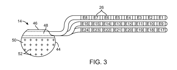
[0019] Fig. 3 is a plan view of an implantable pulse generator (IPG) and three
percutaneous stimulation leads used in the SCS system of Fig. 1;
[0020] Fig. 4 is a plan view of an implantable pulse generator (IPG) and a
surgical
paddle lead used in the SCS system of Fig. 2;
[0021] Figs. 5a and 5b are plan views of different types of frequency
selective
surfaces that can be incorporated into the housing of the IPG of Figs. 3 and
4;
[0022] Fig. 6a-6d are cross-sectional views of different housings that can be
used
for the IPG of Figs. 3 and 4;
[0023] Figs. 7a-7d are plan views of different elements that can be used to
create a
frequency selective surface for the housing of the IPG of Figs. 3 and 4;
[0024] Fig. 8 is a circuit diagram of an impedance load adjustment circuit
that can be
used to adjust the frequency selective surface for the housing of the IPG of
Figs. 3
and 4;
[0025] Fig. 9 is a perspective view of one embodiment of a battery contained
within
the IPG of Figs. 3 and 4; and
[0026] Fig. 10 is a perspective view of one embodiment of a stimulation lead
of Fig.
3.
DETAILED DESCRIPTION OF THE EMBODIMENTS
[0027] The description that follows relates to a Spinal Cord Stimulation (SCS)
system. However, it is to be understood that the while the invention lends
itself well
to applications in SCS, the invention, in its broadest aspects, may not be so
limited.
Rather, the invention may be used with any type of implantable electrical
circuitry
used to stimulate tissue. For example, the present invention may be used as
part of
a pacemaker, a defibrillator, a cochlear stimulator, a retinal stimulator, a
stimulator
configured to produce coordinated limb movement, a cortical stimulator, a deep
brain
stimulator, peripheral nerve stimulator, microstimulator, or in any other
neural
stimulator configured to treat urinary incontinence, sleep apnea, shoulder
sublaxation, headache, etc.
CA 02867896 2014-09-18
WO 2013/158667
PCT/US2013/036817
[0028] Turning first to Fig. 1, an exemplary spinal cord stimulation (SCS)
system 10
generally includes one or more (in this case, three) implantable stimulation
leads 12,
a pulse generating device in the form of an implantable pulse generator (IPG)
14, an
external control device in the form of a remote controller RC 16, a
clinician's
programmer (CP) 18, an external trial stimulator (ETS) 20, and an external
charger
22.
[0029] The IPG 14 is physically connected via one or more lead extensions 24
to the
stimulation leads 12, which carry a plurality of electrodes 26 arranged in an
array.
The stimulation leads 12 are illustrated as percutaneous leads in Fig. 1,
although as
will be described in further detail below, a surgical paddle lead can be used
in place
of the percutaneous leads. As will also be described in further detail below,
the IPG
14 includes pulse generation circuitry that delivers electrical stimulation
energy in the
form of a pulsed electrical waveform (i.e., a temporal series of electrical
pulses) to
the electrode array 26 in accordance with a set of stimulation parameters.
[0030] The ETS 20 may also be physically connected via the percutaneous lead
extensions 28 and external cable 30 to the stimulation leads 12. The ETS 20,
which
has similar pulse generation circuitry as the IPG 14, also delivers electrical
stimulation energy in the form of a pulse electrical waveform to the electrode
array
26 accordance with a set of stimulation parameters. The major difference
between
the ETS 20 and the IPG 14 is that the ETS 20 is a non-implantable device that
is
used on a trial basis after the stimulation leads 12 have been implanted and
prior to
implantation of the IPG 14, to test the responsiveness of the stimulation that
is to be
provided. Thus, any functions described herein with respect to the IPG 14 can
likewise be performed with respect to the ETS 20.
[0031] The RC 16 may be used to telemetrically control the ETS 20 via a bi-
directional RF communications link 32. Once the IPG 14 and stimulation leads
12
are implanted, the RC 16 may be used to telemetrically control the IPG 14 via
a bi-
directional RF communications link 34. Such control allows the IPG 14 to be
turned
on or off and to be programmed with different stimulation parameter sets. The
IPG
14 may also be operated to modify the programmed stimulation parameters to
actively control the characteristics of the electrical stimulation energy
output by the
IPG 14. As will be described in further detail below, the CF 18 provides
clinician
detailed stimulation parameters for programming the IPG 14 and ETS 20 in the
operating room and in follow-up sessions.
6
CA 02867896 2014-09-18
WO 2013/158667
PCT/US2013/036817
[0032] The CF 18 may perform this function by indirectly communicating with
the
IPG 14 or ETS 20, through the RC 16, via an IR communications link 36.
Alternatively, the CF 18 may directly communicate with the IPG 14 or ETS 20
via an
RF communications link (not shown). The clinician detailed stimulation
parameters
provided by the CF 18 are also used to program the RC 16, so that the
stimulation
parameters can be subsequently modified by operation of the RC 16 in a stand-
alone mode (i.e., without the assistance of the CF 18).
[0033] For purposes of brevity, the details of the RC 16, CF 18, ETS 20, and
external charger 22 will not be described herein. Details of exemplary
embodiments
of these devices are disclosed in U.S. Patent No. 6,895,280.
[0034] As shown in Fig. 2, the stimulation leads 12 are implanted within the
spinal
column 42 of a patient 40. The preferred placement of the electrode leads 12
is
adjacent, i.e., resting near, the spinal cord area to be stimulated. Due to
the lack of
space near the location where the electrode leads 12 exit the spinal column
42, the
IPG 14 is generally implanted in a surgically-made pocket either in the
abdomen or
above the buttocks. The IPG 14 may, of course, also be implanted in other
locations
of the patient's body. The lead extensions 24 facilitate locating the IPG 14
away
from the exit point of the electrode leads 12. As there shown, the CF 18
communicates with the IPG 14 via the RC 16.
[0035] Referring now to Fig. 3, the external features of the stimulation leads
12 and
the IPG 14 will be briefly described. Each of the stimulation leads 12 has
eight
electrodes 26 (respectively labeled E1-E8, E9-E16, and E17-E24). The actual
number and shape of leads and electrodes will, of course, vary according to
the
intended application. Further details describing the construction and method
of
manufacturing percutaneous stimulation leads are disclosed in U.S. Patent
Publication Nos. 2007/0168007 and 2007/0168004.
[0036] Alternatively, as illustrated in Fig. 4, the stimulation lead 12 takes
the form of
a surgical paddle lead on which electrodes 26 are arranged in a two-
dimensional
array in three columns (respectively labeled El-E5, E6-E10, and El 1-E15)
along the
axis of the stimulation lead 12. In the illustrated embodiment, five rows of
electrodes
26 are provided, although any number of rows of electrodes can be used. Each
row
of the electrodes 26 is arranged in a line transversely to the axis of the
lead 12. The
actual number of leads and electrodes will, of course, vary according to the
intended
7
CA 02867896 2014-09-18
WO 2013/158667
PCT/US2013/036817
application. Further details regarding the construction and method of
manufacture of
surgical paddle leads are disclosed in U.S. Patent Publication No.
2007/0150036.
[0037] In each of the embodiments illustrated in Figs. 3 and 4, the IPG 14
comprises
an outer case (or housing) 44 for housing the electronics and other components
(described in further detail below). The outer case 44 forms a hermetically
sealed
compartment that protects the internal electronics from the body tissue and
fluids,
while permitting passage of electromagnetic fields used to transmit data
and/or
power. In some cases, the outer case 44 may serve as an electrode. The IPG 14
further comprises a connector 46 to which the proximal ends of the stimulation
leads
12 mate in a manner that electrically couples the electrodes 26 to the
internal
electronics (described in further detail below) within the outer case 44. To
this end,
the connector 46 includes one or more ports (three ports 48 or three
percutaneous
leads or one port for the surgical paddle lead) for receiving the proximal
end(s) of the
stimulation lead(s) 12. In the case where the lead extensions 24 are used, the
port(s) 48 may instead receive the proximal ends of such lead extensions 24.
[0038] The IPG 14 includes pulse generation circuitry that provides electrical
conditioning and stimulation energy in the form of a pulsed electrical
waveform to the
electrode array 26 in accordance with a set of stimulation parameters
programmed
into the IPG 14. Such stimulation parameters may comprise electrode
combinations,
which define the electrodes that are activated as anodes (positive), cathodes
(negative), and turned off (zero), percentage of stimulation energy assigned
to each
electrode (fractionalized electrode configurations), and electrical pulse
parameters,
which define the pulse amplitude (measured in milliamps or volts depending on
whether the IPG 14 supplies constant current or constant voltage to the
electrode
array 26), pulse width (measured in microseconds), pulse rate (measured in
pulses
per second), and burst rate (measured as the stimulation on duration X and
stimulation off duration Y).
[0039] Additional details concerning the above-described and other IPGs may be
found in U.S. Patent No. 6,516,227, U.S. Patent Publication Nos. 2003/0139781
and
2005/0267546. It should be noted that rather than an IPG, the system 10 may
alternatively utilize an implantable receiver-stimulator (not shown) connected
to
leads 12. In this case, the power source, e.g., a battery, for powering the
implanted
receiver, as well as control circuitry to command the receiver-stimulator,
will be
contained in an external controller inductively coupled to the receiver-
stimulator via
8
CA 02867896 2014-09-18
WO 2013/158667
PCT/US2013/036817
an electromagnetic link. Data/power signals are transcutaneously coupled from
a
cable-connected transmission coil placed over the implanted receiver-
stimulator.
The implanted receiver-stimulator receives the signal and generates the
stimulation
in accordance with the control signals.
[0040] Significantly, the outer case 44 is constructed in a manner that
creates a
Frequency Selective Surface (FSS) that, when exposed to electromagnetic
radiation,
generates a scattered wave with a prescribed frequency response. Thus, the FSS
serves as a filter for electromagnetic energy, and in particular, is capable
of reflecting
at least a portion of energy at a first frequency (e.g., electromagnetic
fields emitted
during an MRI) that are incident on the case 44, while passing at least a
portion of
energy of a second frequency incident on the case 44 (e.g., programming
signals or
charging energy) to the necessary componentry contained in the case 44, e.g.,
an
antenna, such as a coil for receiving programming signals and/or charging
energy).
[0041] Preferably, the energy that is reflected is greater than 10 MHz, which
will
typically encompass typical RF frequencies used in MRI scanners (e.g., 64 MHz
and
128 MHz), while the energy that is passed is less than 200 KHz, which will
typically
encompass RF frequencies used in programming signals and charging energy
(e.g.,
84 KHz and 125 KHz, respectively). It is preferable that a substantial amount
of the
energy at the first frequency be reflected, and that a substantial amount of
the
energy at the second frequency be passed. In an optional embodiment, the
energy
that is reflected is also less than 40 KHz, which will typically encompass
typical
gradient fields used in MRI scanners (e.g., 100 Hz to 30 KHz). For the
reflection
coefficient (i.e., the percentage of reflected energy divided by incident
energy) is
preferably greater than 0.5, and more preferably greater than 0.75, whereas
the
transmission coefficient (i.e., the percentage of transmitted energy divided
by
incident energy) is preferably greater than 0.5, and more preferably greater
than
0.75.
[0042] The case 44 includes a substrate structure 50 and a two-dimensional
array of
elements 52 disposed on the substrate structure 50, thereby creating the FSS,
which
can be generally of two types. In particular, a "Type A" FSS is shown in Fig.
5a, in
which the substrate structure 50 is composed of a dielectric material, while
the
elements 52 are composed of an electrically conductive material. In Fig. 5b, a
"Type
B" FSS is shown, in which the substrate structure 50 is composed of an
electrically
conductive material, while the elements 52 are composed of a dielectric
material.
9
CA 02867896 2014-09-18
WO 2013/158667
PCT/US2013/036817
The dielectric material may be, e.g., ceramic or plastic, whereas the
electrically
conductive material, may be, e.g., metal, such as titanium.
[0043] The Type A surface has a complimentary response compared to Type B
surface.
[0044] For example, if the element is a patch, the Type A FSS has a capacitive
surface, and thus, exhibits a low-pass characteristic, such that the FSS
passes
energy at lower frequencies, while reflecting energy at high frequencies. The
Type B
FSS has an inductive surface, and thus, exhibits a low-pass characteristic,
such that
the FSS passes energy at lower frequencies, while reflecting energy at high
frequencies. Thus, the Type A FSS is particularly useful to reflect the higher
frequency MRI electromagnetic fields, while passing the lower frequency
programming signals and/or charging energy, whereas the Type B FSS is
particularly useful to reflect the undesirable energy associated with lower
frequencies, while passing the higher frequency programming signals and/or
charging energy.
[0045] In another example, if the element is a cross-dipole, it can be modeled
as a
shunt element, comprising of series inductor and capacitor between the input
and
output. At resonance, this will lead to a complete reflection, thereby giving
the
surface a band-stop response. Thus, the Type A FSS surface with cross dipoles
will
be particularly useful in reflecting the higher frequency MRI electromagnetic
fields,
while passing the lower frequency energy. On the other hand, the Type B FSS
surface will have a band-pass response, and thus will be particularly useful
to reflect
the undesirable energy associated with lower frequencies, while passing the
higher
frequency programming signals and/or charging energy.
[0046] The reflection/transmission coefficient and frequencies of the energy
that is
reflected/transmitted depend upon the type of element 52 (e.g., size, shape,
loading,
and orientation), distance between the elements 52 in both directions (x- and
y-
directions), conductivity of the elements 52 (which increases the
reflectivity), and
whether which of the substrate structure 50 and elements 52 is composed of a
dielectric material, and which one is composed of an electrically conductive
material.
[0047] The effective length of the elements 52 is preferably a half-wavelength
at the
frequency of the energy intended to be reflected in the case of a Type A FSS,
and a
half-wavelength at the frequency of the energy intended to be passed in the
case of
a Type B FSS. In this case, the coupling between elements 52 and the incident
CA 02867896 2014-09-18
WO 2013/158667
PCT/US2013/036817
electromagnetic energy nominally reaches its highest level at the fundamental
frequency where the effective length of the elements 52 is a half wavelength.
In
order to decrease the size of the elements 52, metamaterial based FSS
techniques
described in Metamaterial-Inspired Frequency-Selective Surfaces, Farhad
Bayatpur,
University of Michigan (2009), can be used. As a general rule, the greater the
spacing between the elements 52 is, the narrower the bandwidth of the energy
that
is reflected or passed, and the less the spacing between the elements 52 is,
the
wider the bandwidth of the energy that is reflected or passed.
[0048] The substrate structure 50 and array of elements 52 may be arranged in
any
one or more of a variety of ways to create the FSS. In the preferred
embodiment,
the array of elements 52 repeat in a periodic fashion, and the elements 52 are
identical in geometry and have a uniform distance between each other. The
elements 52 may be disposed on the substrate structure 50 in any one of a
variety of
manners, depending on whether FSS is a Type A FSS or a Type B FSS.
[0049] As one example shown in Fig. 6a, in the case of a Type A FSS, openings
in
the shape of the elements 52 can be partially formed in the dielectric
substrate
structure 50 in accordance with the desired pattern using a conventional
technique,
such as molding, and then the electrically conductive elements 52 can be
disposed
in the openings using a conventional technique, such as ion beam deposition.
As
shown in Fig. 6a, the electrically conductive elements 52 are flush with the
surface of
the dielectric substrate structure 50. Alternatively, as shown in Fig. 6b, the
electrically conductive elements 52 may be raised above the surface of the
dielectric
substrate structure 50, thereby creating a relief pattern on the case 44. As
another
example shown in Fig. 6c, in the case of a Type A FSS, the electrically
conductive
elements 52 can be formed on the surface of the dielectric substrate structure
50 in
the desired pattern, using a conventional technique, such as photochemical
etching.
As still another example shown in Fig. 6d, in the case of a Type B FSS,
openings in
the shape of the elements 52 can be completely formed through the dielectric
substrate structure 50 in accordance with the desired pattern using a
conventional
technique, such as punching, and then the electrically conductive elements 52
can
be disposed in the openings using a conventional technique, such as injection
molding.
[0050] Referring to Figs. 7a-7d, four different types of exemplary elements 52
will
now be described. Notably, the types of elements that can be used in the
present
11
CA 02867896 2014-09-18
WO 2013/158667
PCT/US2013/036817
invention should not be limited to those illustrated in Figs. 7a-7d. For
example, the
elements may take the form of rectangles (either solid or loops), Jerusalem
crosses,
three- or four-legged dipoles, meandering lines, zig-zags, etc.
[0051] In Fig. 7a, the element 52a takes the form of a loaded linear dipole.
In this
example, the element 52a includes two co-linear sub-elements 54 that are
coupled
to each other through an impedance load 56. Notably, in order to maximum the
reflection coefficient of the FSS illustrated in Fig. 7a, it is preferable
that the
orientation of the electromagnetic waves in the energy designed to be
reflected be
oriented parallel with the orientation of the dipole element 52a.
[0052] Modification of the impedance load 56 will allow tuning of the FSS. For
example, the inductance or capacitance of the impedance load 56 may be
modified
to change the frequency of the energy that is reflected/transmitted, while the
resistance of the impedance lead 106 may be modified to change the bandwidth
of
the frequency range of the energy that is reflected/transmitted.
[0053] In Fig. 7b, the element 52b takes the form of a crossed-dipole. In this
example, the element 52b includes two orthogonal sub-elements 58, which
maximizes the reflection coefficient of the FSS for any orientation of the
electromagnetic waves in the energy incident on the FSS. That is, any
electromagnetic wave in the energy designed to be reflected will be broken
into
orthogonal components by the sub-elements 58.
[0054] In Fig. 7c, the element 52c takes the form of a loop. In this example,
the
circular element 52c interacts with the magnetic component of the
electromagnetic
wave in any orientation.
[0055] In Fig. 7d, the element 52d takes the form of a bow-tie. In this
example, the
element 52d includes two orthogonal sub-elements 60 and two parallel sub-
elements
62 that couple the ends of the sub-elements 60 together. Due to the multiple
sub-
elements, the element 52d reflects energy over a broader frequency range.
[0056] Any of the elements 52 described above may be loaded by different
lumped
combination of components to create an impedance load, such as the impedance
load 56 illustrated in Fig. 7a. Any of these impedance loads may
advantageously be
dynamically adjustable via signaling by an electronic controller, thereby
providing a
means to selectively reflect energy of different frequencies. For example, if
a 1.5
Tesla MRI scanner is used, the impedance load can be modified, such that
energy at
a frequency of 64 MHz is reflected, whereas if a 3 Tesla MRI scanner is used,
the
12
CA 02867896 2014-09-18
WO 2013/158667
PCT/US2013/036817
impedance load can be modified, such that energy at a frequency of 128 MHz is
reflected. A signal transmitted from the RC 16 or the CF 18 can prompt an
electronic controller contained within the IPG 14 to adjust the impedance
load.
[0057] In one example illustrated in Fig. 8, an adjustable impedance load 62
comprises a pair of capacitors Cl, C2 coupled in parallel to each other
between
terminals (not shown) of the respective element 52, with a switch S in series
with the
capacitor C2. The switch S may be selectively opened and closed in response to
a
signal generated by an electronic controller 64 contained within the IPG 14.
When
the switch S is open, only the capacitor Cl is coupled to the respective
element 52,
thereby reflecting energy at a higher frequency (e.g.,128 MHz). In contrast,
when
the switch S is closed, both capacitors Cl and C2 are coupled to the
respective
element 52, thereby reflecting energy at a lower frequency (e.g., 64 MHz).
[0058] Although the FSS has been described as being associated with the case
44
of the IPG 14, it should be appreciated that an FSS can be associated with
other
components of the IPG 14 or even other components of the SCS system 10.
[0059] For example, if the antenna is behind the battery, it may be useful to
use an
FSS for the battery in order to reflect MRI electromagnetic energy while
passing
programming signals and/or charging energy to the antenna. For example,
referring
to Fig. 9, a battery 66 may comprise a case 68 (or housing), which includes a
substrate structure 70 and a two-dimensional array of elements 72 disposed on
the
substrate structure 70 to form an FSS capable of reflecting at least a portion
of
energy of the first frequency incident on the case 68, while passing at least
a portion
of the energy of the second frequency to antenna. The FSS may be similar to
the
Type A FSS illustrated in Fig. 5a or the Type B FSS illustrated in Fig. 5b.
[0060] As another example, referring to Fig. 10, each of the stimulation leads
12
may comprise an outer layer 78 (or housing), which includes a tubular
substrate
structure 80 and a two-dimensional array of elements 82 disposed on the
substrate
structure 80 to form an FSS capable of reflecting at least a portion of energy
of the
first frequency incident on the outer layer 78. The FSS may be similar to the
Type A
FSS illustrated in Fig. 5a.
[0061] Although the afore-mentioned technique has been described in the
context of
an MRI, it should be appreciated that this technique can be used to reflect
other
electromagnetic energy generated by any source that could be harmful to the
patient
or electronic componentry of the SCS system 10.
13
CA 02867896 2014-09-18
WO 2013/158667
PCT/US2013/036817
[0062] Although particular embodiments of the present inventions have been
shown
and described, it will be understood that it is not intended to limit the
present
inventions to the preferred embodiments, and it will be obvious to those
skilled in the
art that various changes and modifications may be made without departing from
the
spirit and scope of the present inventions. Thus, the present inventions are
intended
to cover alternatives, modifications, and equivalents, which may be included
within
the spirit and scope of the present inventions as defined by the claims.
14