Note: Descriptions are shown in the official language in which they were submitted.
TITLE OF INVENTION
Methods For Thick Film Thermoelectric Device Fabrication
Inventor: Ronald Petkie, of Fort Collins, CO, US
Assignee: Berken Energy, LLC, Fort Collins, CO, US
Filed: January 31, 2014
[0001] Deleted.
U.S. PATENT DOCUMENTS
[0002] US 4,902,648 2/1990 Ohta et al
[0003] US 5,103,286 4/1992 Ohta et al
[0004]US5,108,515 4/1992 Ohta et al
[0005]US5,246,504 9/1993 Ohta et al
[0006]US5,318,743 6/1994 Tokiai et al
[0007JUS5,817,188 10/1998 Yahatz et al
[0008]US6,100,463 8/2000 Ladd et al
[0009]U56,103,967 8/2000 Cauchy et al.
Other Publications
[0010]Walton, Principles of thick film materials formulation, The Radio and
Electronic Engineer, Vol. 45, No.3, March 1975, p. 139 - 143
1
CA 2868197 2018-11-29
CA 02868197 2014-10-22
[0011]Min, Thermoelectric Module Design Theories, Rowe, David Michael, ed.
Thermoelectrics Handbook: Macro to Nano, CRC press, 2006, Ch 11
[0012]Ohta et al, Characteristics of (Bi, Sb)2 (Te, Se)3 Based Thick-Film
Thermoelectric Elements for Power Generation, Electrical Engineering in Japan,
Vol. 110, No. 4 , 1990, p. 213-219
[0013]Markowski et al, Thick-film thermoelectric microgenerators based on
nickel-,
silver-and PdAg-based compositions, Electronics Technology, 30th International
Spring Seminar, IEEE, 2007, p. 223-228
[0014]Xi et al, Fabrication of Thermoelectric Modules Using Thermoelectric
Pastes
and an Additive Technology, Mat. Res. Soc. Symp. Proc. Vol. 545, 1999, p. 143
[0015]Navone et al, Development of (Bi,Sb)2(Te,Se)3-Based Thermoelectric
Modules by a Screen-Printing Process, Journal of Electronic Materials, Vol.
39, No.
9,2010, p. 1755¨ 1759
[0016]Navone et al, Optimization and Fabrication of a Thick Printed
Thermoelectric
Device, Journal of ELECTRONIC MATERIALS, Vol. 40, No. 5, 2011, p. 789 ¨ 793
2
CA 02868197 2014-10-22
[0017'] Lee et al, Thin-Film Thermoelectric Module for Power Generator
Applications
Using a Screen-Printing Method, Journal of Electronic Materials, Vol. 40, No.
5,
2011, p. 615 ¨ 619
[00181Lee et at, Thermoelectric properties of screen-printed ZnSb film, Thin
Solid
Films, Volume 519, Issue 16, 1 June 2011, p. 5441-5443
[00191Madan et at, Printed Se-Doped MA n-Type Bi2Te3 Thick-Film Thermoelectric
Generators, Journal of Electronic Materials S, Vol. 41, No. 6, 2012, p. 1481 -
1486
[00201 Kim et al, Fabrication and Characterization of Thermoelectric Thick
Film
Prepared from p-Type Bismuth Telluride Nanopowders, Journal of Nanoscience
and Nanotechnology, Vol. 12, p. 1577-1580, 2012
[0021]We et al, Development of a Measurement Method for the Thermal
Conductivity of a Thick Film Prepared by a Screen-Printing Technique, Journal
of
Electronic Materials, Vol. 41, No. 6, 2012, p. 1170 ¨ 1176
[0022]We et al, Improvement of thermoelectric properties of screen-printed
Bi2Te3
thick film by optimization of the annealing process, Journal of Alloys and
Compounds, Volume 552,5 March 2013, p. 107-110
[0023]Related to electrode contact to thermoelectric doped bismuth and
antimony
telluride for thermoelectric devices
3
CA 02868197 2014-10-22
[00241Drabkin, I. A., L. B. Ershova, Electrical Contact Resistance in
Thermoelectric
Pellets Based on Bi-Sb Chalcogenides, no year, month, or source given on web
[0025]Li et al, Interface Microstructure and Performance of Sb Contacts in
Bismuth
Telluride-Based Thermoelectric Elements, Journal of Electronic Materials, Vol.
42,
No. 6, 2013, p. 1219- 1224
[0026]Lin et al, Barrier/bonding layers on bismuth telluride (Bi2Te3) for high
temperature thermoelectric modules, J Mater Sci: Mater Electron (2011) 22: p.
1313-1320.
[0027]Liao et al, Effect of Interfacial Compound Formation on Contact
Resistivity of
Soldered Junctions Between Bismuth Telluride-Based Thermoelements and
Copper, Electrochem. Solid-State Lett. 2007, Volume 10, Issue 9, p. P23 - P25
STATEMENT REGARDING FEDERALLY SPONSORED RESEARCH OR
DEVELOPMENT
Not Applicable
REFERENCE TO SEQUENCE LISTING, A TABLE, OR A COMPUTER PROGRAM
LISTING COMPACT DISC APPENDIX
Not Applicable
4
CA 02868197 2014-10-22
BACKGROUND OF THE INVENTION
[0028]1. Field of the invention
[0029]The present invention relates generally to fabrication of solid state
electron
devices by methods of thick film deposition and subsequent processing, which
provides versatility and economic high volume production. The methods are
applied
to thermoelectric devices to provide advantages towards ultimately lowering
the
cost per watt for energy harvesting or thermoelectric coolers.
[0030] 2. Description of the related art
[0031] Walton discusses the general aspects of thick films and their
formulation.
For the formulation of thick film pastes, powdered material of metal and/or
glass are
mixed until homogenous with a vehicle. When the vehicle and solid state
powders
are combined in the appropriate volume ratios, a thixotropic paste results
which can
be screen or stencil printed onto substrates. For some specific applications,
the
vehicle is a polymer with a molecular weight that yields the desired
thixotropic
properties required for printing when mixed with a powder that is chemically
inert
with the polymer. In many cases, the vehicle is a polymer can be poly-methyl
methacrylate, ethyl cellulose, or more recently, methyl styrene. Methyl
styrene is a
polymer that completely burns off without residue at 350 C. This complete
volatilization is important in the fabrication of thermoelectric thick films,
where purity
is of importance for electrical and thermal properties, as is well-known in
the field of
thermoelectric devices, especially for power generation. Conventional thick
film
CA 02868197 2014-10-22
structures for conductors and resistors are generally printed on electrically
insulating substrates such as alumina or other ceramic materials, and
electrical
conduction is parallel to the substrate. In the case of thermoelectric
devices, at
least in this invention, electrical conducting substrates are used, and
conduction is
vertical to the substrate. Thus, the two properties of cohesion within the
thick film
and adhesion to the substrate are important, as cohesion determines the
electrical
and thermal performance critical to device performance, and adhesion is
related to
contact resistance, which can directly affect conversion efficiency.
[0032]Research in thick film methods have been reported, though there has been
no progress in developing a process by which the semiconductor remains pure or
is
directly bonded to the metal substrate. Ohta et al [3) first published work on
thermoelectric thick films of the same kind as in this invention, but a glass
frit of
lead oxide was usually added and the films were not densified by pressure, nor
are
there any claims in the patents issued to Ohta or Tokiai similar as reported
in this
invention. Markowski et al used metal inks, and not the conventional doped
semiconductors as are common today.
[00331Xi et al used an epoxy resin as a binder, while Navone et al used a 2%
by
weight polystyrene. In Navone's work, even though a densification process was
reported, the polystyrene wasn't volatilized during the heat treatment at 350
oC, as
this temperature is well below the decomposition temperature. This invention
allows
heat treatment without cracking and delamination of screen printed films
directly
6
CA 02868197 2014-10-22
onto metal substrates because of the high free volume. In addition, no metal
was in
contact with the semiconductor during heat treatment in Navone's work.
MON Lee et al in two publications used a glass binder for ZnSb and CoSb3 and
densified the films by high temperature processing which resulted in porous
films.
Madan et al used an 2% by weight epoxy binder with the thermoelectric
materials
that remained in the thick films. Kim et al removed the organic binder and
used hot
pressing for densification of the thick films on alumina substrates in a
hydrogen
atmosphere, hence the structures were not metallized during this high
temperature
processing. We et al printed Bi2Te3 powders mixed with a glass binder onto
oxidized silicon wafers and densified by sintering without applying pressure,
resulting in relatively porous films.
[0035INo one has reported a direct bond process for fabricating densified
thermoelectric semiconductor thick films on metal substrates as provided in
this
invention. There is a need for such a process in order to lead to high volume
manufacturing of thermoelectric device applications at lower cost.
BRIEF SUMMARY OF THE INVENTION
[0036] An object of the present invention is to provide a method by which to
fabricate thick films in a manner that reduces reactions between the thick
film and
the substrate on which it is deposited by producing a layer with a high free
volume
7
CA 02868197 2014-10-22
after vehicle volatilization. The layer is heated and during the
volatilization process
becomes sintered such that it acquires sufficient structural integrity for
further
processing. The thick film can be densified by pressing to obtain desired
material
properties such as electrical and thermal conductivity, thereby providing a
direct
bond process of a thick film to a substrate with sufficient chemical and/or
mechanical adhesion and with limited reaction at the thick film ¨ metal
interface.
[0037]Another object of the present invention is to provide multi-layered
thick films
with limited interdiffusion at their interfaces and on their substrate through
high free
volume in an intermediate state prior to densification by pressing, as given
above.
Such multi-layered thick films can be printed and dried sequentially, heated
to
volatilize the vehicle, and the remaining solid state constituents in the
individual
layers are sintered or melted and retain their separateness as layers during
the
heat treatment, thus forming a direct bond multilayered thick film.
[0038JA further object of the present invention is to provide an example of an
application in the production of thermoelectric devices, where a primary
adhesion
layer such as a solder, is first deposited followed by a thermoelectric layer,
thus
forming a thermoelectric layer with a single electrode.
[0039]A still further object of the present invention is to provide a two-
electrode
thermoelectric device by plating a counter electrode on the semiconductor
after a
8
CA 02868197 2014-10-22
direct bond process, or alternately by combining two single electrode
thermoelectric
devices under pressure and heat.
[0040]The general process is outlined and can be applied for any materials
system
where there is a fortuitous coincidence of particular material properties,
including
but not limited to, melting temperatures, vapor pressures, and favorable
electrical
and thermal properties.
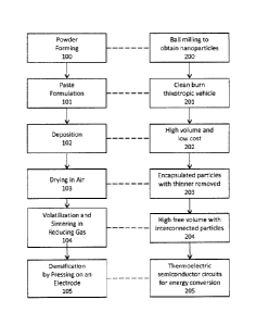
BRIEF DESCRIPTION OF THE SEVERAL VIEWS OF THE DRAWING
[0041] Figure 1 describes the overall process steps of the invention.
[0042] Figure 2 illustrates a cross section of a single layered thick film
directly
bonded to a metal substrate, a single electrode.
[0043] Figure 3 illustrates a multi-layered thick film on a single electrode,
where the
layer next to the metal foil, is a bonding layer such as a solder alloy.
[0044] Figure 4 illustrates a multi-layered thick film, where there is a third
thick film
to provide another bonding layer, such as a solder alloy.
[0045]Figure 5 illustrates a device with an electrode on the top and bottom of
the
stack to form an electron device.
9
CA 02868197 2014-10-22
DETAILED DESCRIPTION OF THE INVENTION
[0046] The following description presents various inventions, and example
embodiments thereof. The various inventions and examples described can be
useful alone or in combinations.
[0047]Fig. 1 is an illustration of the discrete process steps relevant to the
present
invention. Such a process would lead to a progression to discrete
thermoelectric
devices and modules for energy conversion in high volume production, since
thick
film technology by screen or stencil printing is well-established. As provided
by Min,
the thicknesses of discrete p or n type devices for thermoelectric
applications can
be chosen for maximum power or maximum efficiency. For energy harvesting from
heat, the choice is to design in accordance with maximum power, which requires
devices that are thinner than those for maximum conversion efficiency.
Discrete
devices can be fabricated by either a semiconductor 'pellet' [US 5,318,743] or
thick
film screen printing as given in the several publications cited. Pellets are
typically
greater than 0.5 mm in thickness, while thick films are typically greater than
0.1 mm
and less than 0.5 mm.
[0048]Embodiments of the present invention can lower the cost of
thermoelectric
generators (TEGs), since thick film technology is easily applied to high
volume
production of TEG modules, leading to a lower cost per watt in energy
conversion.
Such a cost advantage is especially important for geothermal applications
leading
CA 02868197 2014-10-22
to power plants wherever a hot spring can supply sufficient water flow and
heat on
a continual basis. Other applications include the capture of waste heat in
industrial
environments for conversion to electrical energy.
[0049] These TEGs are can be operated at about 100 ¨ 200 C on the hot side and
room temperature or below on the cold side, or in a manner that provides about
100
C temperature difference between the hot and cold sides. The optimized
operating
temperature can depend on choice of solders, and/or the optimized properties
of
the p and n type semiconductors, and required power output in accordance with
the
temperature difference between the hot and cold side.
[0050] Thick film deposition methodologies allow an approach with several
advantages for prototyping and manufacturing. Thickness and cross-sectional
area
of the thermoelectric elements can be easily modified in accordance with the
design
for maximum power output. Composition (stoichiometry) of the thermoelectric
semiconductor as well as the bonding materials (solder) are easily modified
for
optimization.
[0051]Device layout (lateral dimensions) for circuits are also easily modified
and
space-filling device geometry for the thermoelectric elements is limited only
by the
resolution of the printing apparatus, leading to higher cross-sectional
coverage in
modules, thereby increasing power output.
CA 02868197 2014-10-22
[0052] These advantages above coupled together offer versatility in device
optimization and performance for thermoelectric conversion if a reliable
pathway to
thick film production is found. This approach would also minimize of
electronic
materials deposition waste, allowing more efficient use of available
materials,
especially important for more expensive materials like Tellurium and, in
general,
less materials for recycling. Screen or stencil printing leads to ease of
manufacturing, as they are typically high yield processes and are conducive to
high-volume manufacturing. In addition, there is no vacuum equipment handling
and maintenance, which can be expensive. Fabrication of unit thermocouple
pairs
can be printed by printing sequentially using electroformed stencils if
necessary.
Thermoelectric elements can be connected in series on pre-metalized alumina
substrates and easily scaled to larger arrays consisting of multiple pairs
leading to
modules. Another advantage is that wire sawing of bulk semiconductors is not
necessary, as it is with many thermoelectric products made from bulk
semiconductor crystals. Hence, there this overall fabrication and
microelectronic
packaging strategy can lower the cost/watt over commercially available TEGs
once
the process is optimized for device performance.
[0053]The following thermoelectric semiconductors were used in this work:
N-type semiconductor: N-type Semiconductors typically are composed of
Bismuth Telluride (Si2Te3) and are often doped with Selenium for performance.
The standard composition chosen was Bi2Seo3Te2.7.
12
CA 02868197 2014-10-22
P-type Semiconductor: P-type Semiconductors are typically composed of
Antimony Telluride (Sb2Te3) and are often doped with Bismuth for performance.
The standard composition was Bi ci5Sb1 sTe 3.
[0054]l. Nano-Powder Fabrication:
[0055]A mechanical alloying method was established with planetary ball milling
for
the formulation and fabrication of nanopowders that can be combined with a
polymer vehicle to screen or stencil print these nanopowders. These
nanopowders
are commonly known with standard compositions for p and n type telluride-based
semiconductor for thermoelectric generator applications; known as Bismuth
Telluride (doped with Selenium) and Antimony Telluride (doped with bismuth).
These semiconductors are typically paired in parallel electrically to create a
'p-n
thermocouple pair'.
[0056]Processing of P and N Type Thermoelectric Nanopowders
[0057] Step 1: The individual constituent elements are measured out in the
correct
proportions and loaded into a milling jar with grinding media. Hardened
stainless
steel tungsten carbide jars and media were used provided by Retsch or Across
International. See figure 1, 100 and 200.
13
CA 02868197 2014-10-22
[0058]Step 2: The grinding jars are loaded into a planetary ball mill where
they are
allowed to grind for a set amount of time at a set speed.
[0059]Step 3: The thermoelectric material is separated from the grinding media
with
a sieve and further processed into a thick-film paste. The mesh of the sieve
may
vary in accordance with the desired particle size, which is dependent on the
ball
milling process. The ball milling process is chosen to provide a statistical
range of
desired particle sizes. For screen printing, the sieve must have an aperture
size
that is somewhat less than the screen aperture to ensure efficient printing,
while for
stencil printing the mesh number of the sieve is very flexible. A 500 mesh
sieve will
result in good thick film paste thixotropy when mixed with the proper amount
of
vehicle, as discussed below.
[0060]II. Paste formulation
[0061]General aspects (Figure 1, 101, 201).
[0062] It is well-known in the technology of thick film paste formulation that
solid
particles of a preferred size are mixed with a polymer of a preferred
molecular
weight and a thinner capable of dissolving the polymer. The proper mixing of
these
constituents ideally results in (1) a printable paste and (2) specific
electrical
14
CA 02868197 2014-10-22
properties after the polymer is volatilized. The size of the particles and the
ratio of
the solids volume to polymer volume is important in obtaining the proper
viscosity
and thixotropic properties (Walton). The printed films are typically processed
at
temperatures which sinter the films, and as such, the films are cohesive (have
some internal structural integrity) and adhere to the substrate. The bonding
of the
sintered solids may be both chemical and/or mechanical in nature.
[00631The polymer used here for thermoelectric pastes is commonly known as
methyl styrene (CAS # 25014-31-7), and was purchased from Dupont pre-blended
with an organic thinner (diethylene glycol butyl ether, CAS#112-73-2). Methyl
styrene is known to have a clean burn-off at 350 C and leaves essentially no
noticeable residues after completely volatilization for several minutes
(depending
on the volume tested) at 350 C or greater. After several volatilization
experiments
involving only the thick film polymer vehicles without any solids, the above
information was confirmed. A complete volatilization can help avoid inert
impurities
in the semiconductor thick film legs which affect electrical and thermal
conductivity;
these impurities could otherwise reduce thermoelectric conversion performance.
[0064]A thinning agent is used to adjust the viscosity of the thick film paste
in order
to screen print or stencil print. This thinning agent must be compatible with
the
methyl styrene in terms of solubility, such as Diethylene Glycol Dibutyl
Ether, in
which the polymer is soluble.
CA 02868197 2014-10-22
[0065]Formulation of thick film based thermoelectric devices
[0066]General Aspects (Figure 1, 101, 201).
[0067] The formulation of thick film thermoelectric paste and its subsequent
thermal
processing for the fabrication thermoelectric p and n type devices is in
accordance
with removing the polymer completely to maximize performance. In addition,
since
the polymer is completely volatilized at the process temperatures, the solids
need
(1) to be at least partially sintered, which will provide a minimal degree of
structural
integrity, and (2) have adhesion to the substrate to withstand further
processing.
[0068]Semiconductor Paste
[00691i. A thermoelectric semiconductor paste was formulated with methyl
styrene-based vehicle at about 45 to 65% by volume, with a preferred volume
percentage of 55%. At 55% volume, more favorable and predictable thixotropic
properties (viscosity and printability) result with particle sizes of 45
micron or below.
While larger particle sizes also work, in order to screen print, a particle
mesh size of
325 to 500 or higher is preferred because of limitations in the screen mesh
sizes.
Particle sizes of up to about 200 micron (70 mesh) were tested. Pastes formed
with
larger particles are easily printed using a stencil with apertures that are
larger than
the largest particle size.
16
CA 02868197 2014-10-22
[0070111. The origin for the notion in making the free volume of the
microstructure of
the sintered components about 55% is indicated, at least in part, by
consideration
of interconnected spheres. Though the actual microstructure of the sintered
components consists essentially of randomly interconnected particles which are
not
typically spherical, a spherical particle model suffices to provide an example
of
interconnectedness that can be calculated using geometric formulae. A sphere
of
unit diameter contained within a cube with edges of the same unit dimension is
considered. An array of these spheres, each touching so as to form an
interconnecting organized matrix (such as in a cubic crystal lattice) is
considered for
purposes of modeling an interconnected filamentary network. Each sphere within
a
cube of unit edge length has a volume that is about 52% of the volume of the
cube.
If each sphere represents a solid particle, then the free volume (empty space)
between the spheres is about 48%.
[0071]iii. As it turns out, when making a thixotropic paste from solid
particles and a
suitable polymer vehicle, the thixotropic properties are very suitable at
about the
same volume percentage -50%), thus providing an advantageous method for
making a filamentary interconnected network of sintered particles thorough
printing
and sintering techniques. To further limit interdiffusion at the interface
between the
printed semiconductor layer and the bonding materials, the free volume can be
increased to 55% while making the thixotropic properties even more favorable,
as
was found through practice in the formulation of pastes.
17
CA 02868197 2014-10-22
[0072]iv. In general for any solid powder, the weight percent of solids in the
paste
depends on the overall density of the solids. For Bi2Te3 paste formulation,
for
example, a 55% methyl styrene volume is equivalent to about 12.6% by weight
methyl styrene. The thixotropy and viscosity of the final paste can be
adjustable to
a wide range by controlling the volume or weight percent of the thinner.
[0073] v. As noted above, the vehicle is completely burned off after
volatilization
and the polymer volume is typically 55%. Thus, after volatilization, there is
a free
volume within the remaining solids of 55%. A much lower weight percent of the
polymer, such as 2%, does not result in a high free-volume after thermal
processing, even if the polymer is volatilized. For the case of 8i2Te3, the
free
volume would be about 15%. This aspect of this invention is important and will
be
mentioned later.
[0074J Metal bonding paste formulation
[0075] i. In order to bond the semiconductors to metal substrates, custom
adhesion
promoting bonding materials, also in a printable paste form, were made by
mixing
powder of suitable particle size, vehicle, and a thinner, as with the
semiconductors.
The bonding material in powder form can consist of a single element, mixtures
of
elements and/or, alloys (pre-alloyed binary, ternary, or quaternary solder
alloys).
The printable paste is formulated with the same vehicle, methyl styrene, for a
clean
burn-off. The bonding material is chosen to be compatible by design in
composition
18
CA 02868197 2014-10-22
and melting temperature with a specific substrate and compound semiconductor
element, and have also been formulated similarly to the method of making
thermoelectric semiconductor pastes. These formulations have been tested with
the n and p type semiconductors and nickel substrates and are referred to as
solder
pads.
[0076] ii. The thermal processing of the solder pads may be prior or
concurrent to
the volatilization (sintering) of the semiconductor pastes. When methyl
styrene is
used to formulate the solder pad pastes, and the methyl styrene in the solder
pads
are volatilized at 350 C, the free volume of the solder print post-sintering
appears
to depend on the melting temperature and surface tension of the liquidus phase
of
the elements or alloy at the sintering temperature (minimum 350 C). In some
cases it was observed that the solder pads have a much lower free volume,
indicating consolidation through cornplete melting during volatilization.
[0077] iii. It is preferred that the bonding materials reach a liquidus at
some point in
the thermal processing, as this will likely increase the chemical bonding to
the metal
substrate, possibly through interdiffusion or wettability to the metal
substrate.
[0078]The solder pads can also be fabricated in the typical method using
screen
printable commercially available solder pastes, resulting in zero free volume.
This
method, however, results in more interfacial reaction at the interface between
the
solder material and the semiconductor. In order to fabricate efficient
thermoelectric
19
CA 02868197 2014-10-22
devices, the interfacial reaction between the semiconductor and solder pad in
generally minimized since it affects contact resistance. This interfacial
reaction can
be kept to a minimum through this invention. This aspect will be discussed
later.
[0079] III. Processing of thick film based thermoelectric devices
[0080]Printing I Drying (Figure 1, 102, 103, 202, 203; Figure 2, 300, 302).
[00811i. A 0.5 mil or greater emulsion thickness for a screen, or alternately
as much
as a 10 mil thick stencil, patterned with arrays of rectangular apertures of
varying
size, thick films were printed onto substrates to form thermoelectric pads as
test
structures. Thick films of semiconductor pads ranging from approximately 0.5
and
mil thickness, in accordance with the thickness of the emulsion or stencil,
were
printed with excellent resolution to form test patterns. Such test patterns on
various
substrates were used to determine compatibility of the various metal
substrates
with the semiconductors and optimize the thermal processing. This was
accomplished by measuring the Seebeck coefficient (open circuit voltage) at
100 C
temperature difference as a means of gauging the success given the materials
and
thermal processing scheme. In this manner, feasibility could be readily
determined
for various combinations of test structures without forming a counter
electrode on
the semiconductor.
CA 02868197 2014-10-22
[0082]ii. At this point, the films may be printed over again by registration
to the
existing pattern to increase the thickness of the semiconducting elements
prior to
sintering or add a top bonding pad for contact to a top electrode [302].
Multiple
prints can also be performed before drying. Alternately, and preferred,
adhesion-
promoting materials such as a custom solder alloy [302, 303] as discussed
above
(detailed later) can be printed prior to printing the semiconductor pads. The
n type
and p-type semiconductors were used without such a layer in these experiments
had robust adhesion to nickel after pressing. Additionally, there is a well-
known
reaction between nickel and tellurium which is detrimental to contact
resistance,
thus it is preferred that an intermediate layer, or solder layer, be printed
prior to the
semiconductor, hence this is the preferred method. This interlayer material
between
the metal substrate [(301] and the semiconductor [300] (source of
thermoelectric
effect) is easily tuned in terms of composition by material design to have the
proper
melting temperature that is equal to or less than the sintering temperature.
The
sintering temperature is dictated by the volatilization temperature of the
methyl
styrene, which is a minimum of 350 C.
[0083]iii. Arrays of solder and semiconductor pads were printed and dried
sequentially with registration of the semiconductor pad to be centered within
the
printed solder pad. The substrate in most cases was nickel with dimensions
typically 36mm x 36 mm x 5 mil and 27 mm x 34 mm x 5 mil. The 5 mil thickness
was found to be the most suitable in terms of substrate strength and
subsequent
processing. The substrate thickness was in the range of 1 mil to 10 mil. After
21
CA 02868197 2014-10-22
printing, the thick films were dried at about 100¨ 150 C to volatilize the
thinner, at
which point there is only the bonding pad powder material (solder-like) or
semiconductor powder encapsulated by the polymer. This 'green' state protects
the
powders from oxidizing in atmosphere.
[0084]iv. Test patterns of thick films of approximately 0.5 and 10 mil for the
solder
and semiconductor pads, respectively, in accordance with the thickness of the
screen emulsion or stencil, were printed with excellent resolution and
overlay.
[0085]v. In order to gauge the value Seebeck voltages of experimental test
structures, a baseline Seebeck voltage is determined for a given semiconductor
powder. A sample of the pure semiconductor powder used in making the paste is
pressed at several tons, forming a thin pellet with about the same area that
is
printed with the paste. The Seebeck voltage for this powder is measured at 100
C
temperature difference. The Seebeck coefficient is used as a means by which
evaluate the success of the materials and processing.
[0086]vi. Alternately, the above films may be sintered, pressed, and
additional films,
not necessarily of the same material (solder alloys), can be printed over the
pads
by registration to the pattern of pads.
=
22
CA 02868197 2014-10-22
[0087]vii. Any conceivable variation of the above materials printing, drying,
pressing, reprinting may be permissible in terms of fabricating a
thermoelectric
device structure as discussed later. See Figures 2-5.
[0088]Sintering (Figure 1, 104, 204):
[0089]This process includes volatilization of the methyl styrene polymer and
sintering of the semiconductor simultaneously.
[0090] i. The volatilization involved 350 C for at least 26 minutes, given
the nature
of the furnace, with the prints fully exposed to a gas ambient comprised of
about
5% hydrogen in argon with at least 3 liters per minute flow rate in a 6 inch
diameter
quartz furnace tube. By exposing the printed structures (square pads), the
methyl
styrene is volatilized in the least amount of time. Without a direct open
exposure to
the gaseous ambient, the volatilization can require longer times. It is
important to
minimize the time at the peak temperature after volatilization of the polymer,
since
this will allow more time for interfacial diffusion between materials even
with
considerable free volume in the thick film layers.
[0091]ii. The pattern definition of the films is retained, as the process
temperature is
well below the melting point of both types of the semiconductors, and the
microstructure of the pads consists of a sintered powder. The sintered powder
has
sufficiently interconnected grains, or filaments, such that the printed pads
have
23
CA 02868197 2014-10-22
enough structural integrity to support itself. It appears that the sintered
powder is
structurally composed of a filamentary interconnected network that is
sufficiently
strong enough to retain its shape for further processing, which includes
consolidation by pressing. That is, the printed pads have sufficient adhesion
to the
substrate, or solder pad, and cohesion within itself to remain intact
regardless of
substrate orientation. That is, for the proper choice of materials, the
sintered films
with the printed pads may be turned upside down with the pads remaining in
place.
[0092]iii. The choice of methyl styrene and its clean burn-off allow for the
fabrication
a printed materials which have essentially the same purity as the original
material
only with relatively high free volume (average density is very low). We chose
to call
this microstructure a filamentary interconnected network, or FIN. The sintered
microstructure of the semiconductor has a free volume estimated to be over 50%
as mentioned earlier. For the solder layer, it is estimated to be the same or
somewhat less, depending upon the degree of melting and agglomeration during
thermal processing, in which case there can be consolidation and the free
volume,
if any, is considerably reduced. The fact that the semiconductor materials
sinter,
forming a cohesive microstructure, and the fact that the some semiconductor
materials can be bonded to the substrate through their own adhesion, or
preferentially the adhesion is assisted by first printing adhesive materials,
such as
solders, allow for unique thermoelectric semiconductor pads on metal foil or
metallized substrates, such as copper clad alumina or anodized aluminum.
24
CA 02868197 2014-10-22
[0093]iv. Because the free volume is significant, the effective coefficient of
thermal
expansion of the thick films during sintering essentially matches that of the
substrate, since the FIN can accommodate by expanding or contracting and still
remain intact.
[0094]v. The powder, during the thermal processing, forms an interconnected
microstructure with sufficient cohesiveness. The cohesive strength allows the
sintered thick films to be further processed conveniently, which is
consolidation
through pressing, without a binding agent such as glass. Glasses (frits) are
commonly used in thick film formulation to provide a sintering agent which
binds
metal particles together, for example. These binding agents are generally non-
conductive and increase the resistivity of the processed thick film, while at
the same
sufficiently melting or softening enough to provide consolidation after the
polymer
vehicle is volatilized. The nanoparticles powders of the semiconductors are
mechanically alloyed by ball-milling.
[0095]vi. The thermal process is essentially a non-densification sintering
process
which involves at atomic diffusion in order to join at least of the particles
together to
form an interconnected microstructure. Some partial melting could occur,
especially
for the smaller particles, due to structural melting point depression as
described by
the Gibbs-Thomson effect. In this case, the melting point of the
semiconductors is
reduced as the particle size is reduced. In addition to this effect, smaller
particles
CA 02868197 2014-10-22
are expected to have a higher vapor pressure at the thermal process
temperature,
hence atomic movement is also enhanced for nanoparticles of the semiconductor.
[0096]vii. It has been experimentally observed that a discoloration
surrounding the
thick film semiconductor pads, which is form the elements with higher vapor
pressures during thermal processing. The discoloration is the reaction with
the
nickel substrate. Since antimony and tellurium have the highest vapor
pressures,
the discoloration of p-type thick films usually is more noticeable.
[0097]viii. Considered also is the melting temperatures of bismuth and
antimony
telluride, which are 585 C and 620 C, respectively, with respect to thermal
processing. Since the thermal process temperature must be at least 350 C to
volatilize the methyl styrene, the process temperature is close to 80% of the
melting
temperatures. At temperatures close to the melting point, there is
considerable
kinetics, which also assist in the evolution of the microstructure to form an
interconnected network.
[0098] ix. Thus, there appears to be fortuitous coincidence of certain
material
properties and thermal processing schedules that is an advantage in the
fabrication
of thermoelectric semiconductor thick films. The properties directly related
to the
fabrication involve the coefficient of thermal expansion, vapor pressures of
various
semiconductor elements, chemical reactivity at interfaces, and free volume
which
limits the interfacial reactions. A high temperature process window with a
relatively
26
CA 02868197 2014-10-22
short process time allows fabricating unique thick film thermoelectric
semiconductor
compounds with competitive Seebeck voltage output through screen or stencil
printing, thus allowing low-cost manufacturing.
[0099]x. Methyl styrene volatilizes at 350 C with limited compositional
changes in
semiconductors and leaving pure thermoelectric semiconductor after sintering.
Tellurium and selenium have relatively high vapor pressures, thus it can be
important to minimize process time at higher temperature to avoid
compositional
changes to avoid changing the thermoelectric performance of the
semiconductors.
Though the starting compositions can be modified to compensate for
compositional
changes due to the presence of elements with relatively high vapor pressures
at the
sintering temperature, it can be beneficial to avoid having the elements
condense
on portions of the furnace, which would then increase material lost in
processing.
[00100] xi. Thus,
it is fortuitous that methyl styrene is (1) completely volatilized
within 26 minutes using the equipment above, hence keeping compositional
changes from escaping high vapor pressure elements in the semiconductor
manageable, and (2) the minimizing the interfacial reaction between the
semiconductor and any materials in direct contact due to the high free volume
of
the thick film semiconductor. The volume density of the semiconductor at the
semiconductor-metal interface is 45% (typically), the same amount as the
fraction
of solids in the paste formulation. The bulk density of Bi2Te3 is about 7.7
g/cc,
27
CA 02868197 2014-10-22
giving the effective density of the thick film as -3.5 gicm3 at the interface
which
limits interfacial reaction considerably.
[00101] xii. Sintering of the thermoelectric semiconductor materials can
help to
make the printed nanopowders cohesive, adhesive to the metal foil substrate,
and
optimized for performance. Contact resistance between the semiconductors and
the underlying material (metal foil substrate or solder pad on metal foil)
should be
as low as possible for high performance of the TEG devices, especially thin
thermoelectric semiconductor devices. Pure semiconductor powder can be
sintered
and pressed, as mentioned previously, to make a test pellet for measuring the
Seebeck voltage. Thus far, it has been experimentally established in this work
that
p type semiconductor pellets show an increased Seebeck voltages as the
sintering
temperature is increased from 350 C to 400 C, while n type semiconductor
pellets
show a decreased Seebeck voltages as the sintering temperature is increased to
400 C from about 300 C. Thus, a minimum sintering temperature for
volatilization
of the methyl styrene falls slightly above the optimized sintering
temperatures for n
type material (-300 C) and slightly below the optimized sintering temperature
for p
type materials (400 C). Additional experimentation can be used to optimize
the
thick film process temperatures and overall fabrication methodology, similar
to the
manner in which the sintering temperatures for pellet samples are optimized.
[00102] xiii. The high free volume microstructure of sintered semiconductor
materials (and in some cases solder alloy pads) has the benefit of limiting
28
CA 02868197 2014-10-22
intermediate reaction products formed by interdiffusion at interfaces between
the
solder alloy pad structures or the metal electrode (no solder pad). Though the
chemical nature of intermediates can be estimated through phase diagram
analysis, they introduce another unknown in terms of their electrical and
thermal
properties. Although it is desired to limit the formation and thickness of
intermediates, a minimum thickness is required to promote chemical adhesion
through their formation. Thus, the minimum thickness of the intermediate layer
is
determined by the requirement of sufficient adhesion between the two
contacting
layers. An additional sintering step to induce interdiffusion bonding may be
required
after pressing to ensure adequate bonding of the layers, since the interaction
of
adjacent materials is limited by virtue of high free volume during initial
sintering.
[00103] xiv. Fabrication of single-electrode device structures: The cross-
section of a single-electrode thick film is illustrated in Fig. 2, 300, 301.
[00104] The microstructure is at the state of high free volume and ready to
be
densified. It is shown standing vertically to illustrate the structural
integrity of the
thick film.
[00105] Process Overview Summary
[00106] i. Each layer is screen or stencil printed with appropriate custom
paste.
Substrates were typically 5 mil thick nickel with substrate lateral dimensions
29
CA 02868197 2014-10-22
typically ranging from 2.7-3.6 cm in the form of squares or rectangles. Nickel
[301]
was chosen for its temperature coefficient of linear expansion, availability
as a foil,
and oxidation resistance. Each layer had a dedicated screen or stencil in
order to
deposit a specific thickness with a pattern of square test structures of
varying edge
dimensions. Each screen or stencil formed a set and were registered for
alignment
to one another and used in sequence to form the final device. The solder pads
[302, 3031 were slightly larger than the semiconductor test squares [301] and
the
semiconductor test structures were printed such that they were centered over
the
solder pad square to avoid direct contact with the substrate. The square test
patterns for the semiconductor had edges ranging from 1 to 5 mm, giving 1 to
25
mm2 per test structure. A preliminary polyimide layer (not shown) was
optionally
deposited around each test structure for isolating single test structures.
This layer
provided an electrical insulating layer for combing single electrode devices
without
shorting the electrodes, as there was a tendency for the soft nickel
substrates to
curl at the edges when cut by a scissor. For combining two single electrode
device
halves, an optional final layer of a selected solder was deposited over the
semiconductor prior to sintering.
[00107] ii. Sintering [104]! Pressing processes [105]: Sintering: the high
volume percent of the polymer in the pastes, which is completely volatilized
by
sintering at 350 C for about 30 minutes, allows for a high free volume in the
remaining printed structures after volatilization. This high free volume
introduces
distinct advantages as described above through its microstructure for unique
CA 02868197 2014-10-22
fabrication of layered materials and interfaces in general, with
thermoelectric
devices being a distinct application. The advantages can be summarized as
follows:
[00108] Each layer can be pressed [105] at several tons of pressure after
it is
sintered, or the multiple sequential layers can be printed and dried as a
process
step for each layer, and then sintered and pressed at several tons to complete
a
single-electrode device. Applied pressures here ranged from 1 to 40 tons
depending on total printed semiconductor area. Total semiconductor area
typically
was about 5 cm2 of semiconductor area per substrate. To obtain layers with
near
normal bulk density of the compounds and alloys, about 20 MPa pressure was
applied. (N and P type devices can be optimized separately in terms of
fabrication
processing).
[00109] iii. Because of high free volume of non-pressed layered structures
from printing and sintering together, the amount of volume interaction between
two
FIN microstructure layers is very limited, thus dramatically limiting possibly
undesired intermediate compound formation between two different layers
normally
formed by interdiffusion bonding between two layers. This is especially true
if
neither material is pressed prior to further sintering.
[00110] iv. These FIN microstructures can be permeated with another
material
that is in liquid form and has a low surface tension for modifying the layer.
For
31
CA 02868197 2014-10-22
example, gallium¨indium alloy which has a melting point of about 30 C and is
known to make good contact with these thermoelectric materials.
[00111] v. Printing, sintering, and pressing process may be done in any
manner which facilitates the fabrication of a thermoelectric device, which
includes
using different materials to make 'stacked' thermoelectric devices as
mentioned in
the literature, as long as the materials are sequentially compatible. However,
it is
understood that pressing might only follow the volatilization of the methyl
styrene
following printing in a given sequence of steps to make a new layer.
[00112] Bonding single-electrode. Each discrete device is bonded to the
other
by use of a solder, or the surfaces of the semiconductors can be thermo-
compression bonded at elevated temperatures and pressures. See Fig. 3.
[00113] Experimental samples: See Fig. 4. Screen-printed n type single-
electrode on 36 x 36 mm nickel foil substrate 5 mils in thickness.
Thermoelectric
thicknesses are approximately 100 microns.
[00114] Seebeck voltages were about 16 mV or greater at 100 C temperature
difference. The process for making the thermoelectric thick films was very
repeatable and not optimized.
[00115] Notes on Solder Alloys
32
CA 02868197 2014-10-22
[00116] i. Solder alloys can be custom formulated to have a liquidus state
at a
given process temperature by combining a low melting temperature metals with
high melting temperature element, such as silver or antimony. since wetting
behavior will facilitate interdiffusion bonding between the solder and the
semiconductor and minimize voids at the interface. To achieve this wetting
behavior, a balance between the surface tension of the liquidus, the percent
of
liquidus at the process temperature, and the volume density of the solder
alloy in
the solder pastes will allow for a large variation of microstructural growth
of the
solder layers.
[00117] ii. The solder alloy can be designed to form a liquidus phase that
melts
just below the process sintering temperature by the addition of a metal
element(s),
such as silver, that has a higher melting point than the binary solder. Silver
and
copper, which also have a high thermal and electrical conductivity, will
increase the
melting temperature of solder alloys such as Pb-Sn, Bi-Sn, SbSn, Bi-Sb, etc.,
leading to ternary or quaternary solder alloys. Silver is preferred, as it is
less
reactive than copper by way of experimental observations at this laboratory.
The
additional element or alloy is preferably an element with good electrical and
thermal
conductivity to accommodate high levels of energy conversion efficiency.
[00118] iii. Specific examples tried experimentally, not limited to the
following,
were the addition of silver to Sb5Sn95, Bi-Sn, alloys, and Bi-Sb alloys using
a methyl
33
CA 02868197 2014-10-22
styrene vehicle. Lower melting point binary solder alloys will tend to have
normal
densities after sintering due to agglomeration, and some bonding pads can have
a
larger degree of surface roughness, which can be advantageous for mechanical
adhesion when printing the semiconductors pads.
34