Note: Descriptions are shown in the official language in which they were submitted.
,
CA 2868261
1
CONTINUOUS WHOLE-CHIP 3-DIMENSIONAL DEP CELL SORTER AND RELATED
FABRICATION METHOD
[0001] <deleted>
[0002] <deleted>
BACKGROUND OF THE INVENTION
[0003] Microfluidic devices present a cost-effective mechanism for performing
small-scale fluidic
manipulation on various fluid-entrained samples. For example, some
microfluidic devices may be used
to route, sort, and analyze cells contained in a fluid sample.
[0004] Multilayer soft lithography (MSL) is by far the most widely used
approach for fabricating
microfluidic devices. Numerous devices, from simple monolayer
polydimethylsiloxane (PDMS)
channels to multilayer structures with pneumatically controlled pumps and
valves, have been used to
provide versatile microfluidic functions including liquid delivery, mixing,
and metering. Microfluidic
large-scale integration (mLSI) has been realized in the form of microfluidic
multiplexers to individually
address thousands of valves and hundreds of chambers for conducting complex
and multistep
biochemical analyses, e.g., in lab-on-a-chip devices. Most multilayer PDMS
devices demonstrated so
far are not true 3D microfluidic devices. Although multiple layers of 2D
microfluidic networks can be
stacked, there is
CA 2868261 2019-07-25
CA 02868261 2014-09-23
WO 2013/148865 PCT/US2013/034145
2
typically no interlayer fluid communication due to the difficulty of
fabricating high-
resolution through-layer vias for fluidly connecting different layers in high
yield.
Without through-layer vias, fluid routing and interfacing become complex
issues for
large scale 3D microfluidic networks.
[0005] One function that microfluidic devices may provide is cell or
particulate
sorting. For example, a fluid sample may have a variety of different types of
cells or
particles entrained within, and it may be desirable to isolate or concentrate
cells or
particles of a particular type with respect to the overall sample.
Dielectrophoresis
(DEP) is one of the most commonly used mechanisms exploited to sort cells or
particulates. DEP refers to induced particle motion along an electric field
gradient
due to the interactions between induced electric dipoles of the particles and
the
applied electric field. The DEP force acting on a spherical particle, FDEP,
suspended
in a medium may be expressed as:
DEP = Ire1Re[K(oWVE2
where r is the radius of the particle, K is the Clausius-Mossotti factor, E is
the electric
field strength, co is the angular frequency of the applied field, and Ei is
the dielectric
permittivity of the media. Since the resultant force is dependent on the
electric field
intensity gradient, VE2, the particle can be attracted towards any
inhomogeneities in
the field, created for example by the metallic patches on micropatterned-
templates.
The sign and the effective polarizability of the spherical particle may be
expressed
as:
N
a a,
Re[K] = ________________________ E =S+ _____ e;, + __
6, 2E,
where al is the conductivity of the media and 2 and 02 dielectric
permittivity and
conductivity for the particles. If Re[K] is positive, particles move towards
the strong
electric field regions; in contrast, If Re[K] is negative, particles move to
the low
electric field regions.
CA 02868261 2014-09-23
WO 2013/148865
PCT/US2013/034145
3
[0006] Thus, a cell or particulate subjected to a non-uniform electric field
experiences a force due to DEP effects. The magnitude of the force is
dependent on
various factors, including the dielectric signature of the cell or
particulate, as well as
the frequency of the electric field. Depending on the DEP field used and the
characteristics of the individual cells or particulates subject to the DEP
field, cells or
particulates may experience either positive DEP (experiencing force that urges
the
cell or particulate in the direction of increasing field strength) or negative
DEP
(experiencing force that urges the cell or particulate in a direction opposite
of
increasing field strength). In many cases, the movement of cells or
particulates via
DEP may be practically limited to approximately 100 [irn/s given the
characteristics
of those cells or particulates, the media that are commonly used to transport
them,
and the electrical characteristics of microfluidic systems.
[0007] DEP response of cells or particulates may be altered or enhanced by
tagging
cells or particulates of interest with molecules, e.g., labeled or unlabeled
antibodies,
or beads that are specific to certain cells or particulates of interest. This
may allow
for easier separation of the target cells or particulates using DEP. While
such tagging
can enhance DEP techniques, it is not necessary in many cases.
[0008] Figure 1 depicts one example of a two-dimensional DEP cell sorter 100.
Figure 1 shows only a plan view of a portion of a PDMS layer of the cell
sorter 100; in
actual practice, the PDMS layer would be sandwiched between two plates, e.g.,
glass
plates, that are not shown. The PDMS layer may include a sample channel 102
and a
buffer channel 104 that run parallel to one another and that are separated
from one
another by a thin wall 116. A fluid sample and a buffer may be flowed into the
sorter from, with respect to the orientation of Figure 1, left to right via
their
respective channels. The thin wall 116 may have an opening 118 that permits
fluid
communication between the sample channel 102 and the buffer channel 104.
Patterned electrodes 106 may extend at an angle across the sample channel 102;
a
patterned electrode 106 may be patterned on each of the two plates. An
electromagnetic field may be produced within the sample fluid that is flowed
through the sample channel 102 between patterned electrodes 106 when an
alternating current is used to produce a voltage across the electrodes.
Depending on
CA 02868261 2014-09-23
WO 2013/148865 PCT/US2013/034145
4
the frequency of the electromagnetic field, certain cells, e.g., "square"
cells 110, may
be drawn towards the maximum field strength and "round" cells 108 may be
repulsed or unaffected. The angled nature of the electromagnetic field (due to
the
angle of the patterned electrodes 106) may cause the square cells 110 to be
drawn
towards the buffer channel 104 as the fluid flow in the sample channel 102 and
the
buffer channel 104 progresses, with respect to the orientation of Figure 1,
from left
to right. After the end of the opening 118, the square cells 110 that have
been
shunted towards the buffer channel 104 may flow into a collection channel 112,
whereas the round cells may flow into a waste channel 114.
[0009] Figure 2 depicts another example of a two-dimensional DEP cell sorter
200.
In this case, the cell sorter 200 includes two sample channels 202 that
bracket a
buffer channel 104. A fluid sample may be flowed into the cell sorter 200 via
the
sample channels 202 while a neutral buffer may be flowed into the cell sorter
200 via
the buffer channel 204. The combined buffer/sample fluid flows through a
sorting
region containing a number of patterned electrodes 206. When the patterned
electrodes 206 are powered at a particular frequency, the resulting
electromagnetic
field may cause the square cells 210 to migrate towards the center of the cell
sorter
200, whereas the round cells 208 may migrate towards, or stay in, the outer
edges of
the cell sorter 200. The center-concentrated square cells 210 may then flow
into a
.. collection channel 212, whereas the round cells 208 may flow into waste
channels
214.
[0010] Two-dimensional cell sorters typically have a maximum flow rate beyond
which the cell sorting functionality is lost or significantly impaired. The
forces
produced by DEP, and consequently the rate at which DEP can move cells across
the
flow stream and into position for flow into the collection channels, are
limited by the
size and shape of the electrodes as well as other system characteristics. If
the fluid
flow rate is fast enough that the cells flow past the patterned electrodes
before the
forces produced by the DEP effect can re-position the cells for flow into the
collection channels, then the cells will not be effectively sorted. This
limits the
maximum flow of two-dimensional cell sorters, and, consequently, the maximum
throughput of a two-dimensional cell sorter. Such two-dimensional DEP cell
sorters
CA 02868261 2014-09-23
WO 2013/148865
PCT/US2013/034145
are thus typically limited to maximum flow rates of approximately 1mm/sec,
which,
in turn, limits the throughput of such cell sorters.
SUMMARY
[0011] Details of one or more embodiments of the subject matter described in
this
5 specification are set forth in the accompanying drawings and the
description below.
Other features, aspects, and advantages will become apparent from the
description,
the drawings, and the claims. Note that the relative dimensions of the
following
figures may not be drawn to scale unless specifically indicated as being
scaled
drawings.
[0012] In various aspects, the invention(s) contemplated herein may include,
but
need not be limited to, any one or more of the following embodiments:
[0013] Embodiment 1: A 3-dimensional dielectrophoretic (DEP) sorting device,
the
device including: a first electrode; a second electrode; an electrically-
insulating layer
sandwiched between the first electrode and the second electrode, wherein: the
electrically-insulating layer includes a separation passage with walls
partially
bounded by the first electrode and the second electrode, the electrically-
insulating
layer includes a collection passage smaller than the separation passage in
cross-
sectional thickness and located at an inter-electrode location between the
first
electrode and the second electrode, the separation passage is shaped to
produce an
electromagnetic field that causes a dielectrophoretic effect to draw
responsive cells
or particulates to a location between the first electrode and the second
electrode
that substantially corresponds with the inter-electrode location of the
collection
passage, and the collection passage and the separation passage are configured
such
that cells or particulates drawn to the inter-electrode location between the
first
electrode and the second electrode in the separation passage are then flowed
into
the collection passage.
[0014] Embodiment 2: A 3-dimensional dielectrophoretic (DEP) sorting device,
the
device including: a first electrode; a second electrode; an electrically-
insulating layer
sandwiched between the first electrode and the second electrode, wherein: the
CA 02868261 2014-09-23
WO 2013/148865 PCT/US2013/034145
6
electrically-insulating layer includes: a fluid flow passage, the fluid flow
passage
having a cross-section partially defined by the first electrode and the second
electrode; a first side passage that is parallel to the fluid flow passage
within a DEP-
separation region of the device and separated from the fluid flow passage by a
first
thin, deformable wall; a second side passage that is parallel to the fluid
flow passage
within the DEP-separation region and separated from the fluid flow passage by
a
second thin, deformable wall, wherein: the first side passage and the second
side
passage are hermetically sealed from the fluid flow passage, and application
of
pressurized gas or fluid to the first side passage and the second side passage
causes
the first thin, deformable wall and the second thin, deformable wall to bulge
into the
fluid flow passage.
[0015] Embodiment 3: The 3-dimensional DEP sorting device of embodiment 2,
wherein drawing a vacuum on the first side passage and the second side passage
causes the first thin, deformable wall and the second thin, deformable wall to
bulge
into the side passages.
[0016] Embodiment 4: The 3-dimensional DEP sorting device of embodiment 2 or
embodiment 3, wherein the side passages are filled with a liquid or gel.
[0017] Embodiment 5: The 3-dimensional DEP sorting device of embodiment 4,
wherein the liquid or gel is cured into a solid form after being pressurized,
thus
causing the thin, deformable walls to bulge into the fluid flow passage, or
subjected
to a vacuum, thus causing the thin, deformable walls to bulge into the side
passages.
[0018] Embodiment 6: A 3-dimensional dielectrophoretic (DEP) sorting device,
the
device including: a first electrode layer; a second electrode layer; an
electrically-
insulating layer interposed between the first electrode layer and the second
electrode layer and having a first sub-layer and a second sub-layer; a first
passage
located in the first sub-layer; and a second passage located in the second sub-
layer;
wherein: the first electrode layer, the second electrode layer, and the
electrically-
insulating layer form a substantially planar assembly, the first electrode
layer is on an
opposite side of the first sub-layer from the second layer, the second
electrode layer
CA 02868261 2014-09-23
WO 2013/148865
PCT/US2013/034145
7
is on an opposite side of the second sub-layer from the first layer, the first
passage
and the second passage follow a common path within a DEP separation region of
the
electrically-insulating layer and are in direct fluid communication with one
another
within the DEP separation region, the first passage and the second passage
each
have a different cross-sectional width perpendicular to the common path and
perpendicular to a normal of the substantially planar assembly, and the first
passage
diverges from the second passage in a post-DEP separation region, the post-DEP
separation region located downstream of the DEP separation region.
[0019] Embodiment 7: The 3-dimensional DEP sorting device of embodiment 6,
further including: a third sub-layer of the electrically-insulating layer; a
third passage
located in the third sub-layer, wherein: the second sub-layer is interposed
between
the first sub-layer and the third sub-layer, the third sub-layer is interposed
between
the second sub-layer and the second electrode layer, the third passage follows
the
common path within the DEP separation region and is in direct fluid
communication
.. with the second passage within the DEP separation region, the third passage
has a
cross-sectional width perpendicular to the common path and perpendicular to
the
normal of the substantially planar assembly that is different from the cross-
sectional
width of the second passage, and the third passage diverges from the second
passage in the post-DEP separation region.
[0020] Embodiment 8: The 3-dimensional DEP sorting device of embodiment 7,
wherein the cross-sectional width of the second passage is less than the cross-
sectional widths of the first passage and the third passage.
[0021] Embodiment 9: The 3-dimensional DEP sorting device of embodiment 7,
wherein the cross-sectional width of the second passage is greater than the
cross-
sectional widths of the first passage and the third passage.
[0022] Embodiment 10: The 3-dimensional DEP sorting device of any one of
embodiments 7 through 9, wherein the first passage, the second passage, and
the
third passage are substantially centered over one another in a direction
perpendicular to the common path and parallel to the substantially planar
assembly.
CA 02868261 2014-09-23
WO 2013/148865
PCT/US2013/034145
8
[0023] Embodiment 11: The 3-dimensional DEP sorting device of embodiment 6,
further including one or more additional passages, each located in an
additional sub-
layer, wherein: the one or more additional passages includes a third passage,
the
one or more additional passages follow the common path within the DEP
separation
region of the electrically-insulating layer and are in direct fluid
communication with
one another and the first passage and the second passage within the DEP
separation
region, the one or more additional passages each have a cross-sectional width
perpendicular to the common path and perpendicular to the normal of the
substantially planar assembly, the cross-sectional width of each particular
additional
passage is different from the cross-sectional width of each additional passage
neighboring that particular additional passage, and at least one of the one or
more
additional passages diverges from the second passage in the post-DEP
separation
region.
[0024] Embodiment 12: The 3-dimensional DEP sorting device of any one of
embodiments 6 through 11, wherein the first electrode layer and the second
electrode layer include patterned electrodes in the DEP separation region.
[0025] Embodiment 13: The 3-dimensional DEP sorting device of any one of
embodiments 6 through 11, wherein the first electrode layer and the second
electrode layer are substantially flat plates with electrically-conductive
surfaces
facing the electrically-insulating layer.
[0026] Embodiment 14: The 3-dimensional DEP sorting device of embodiment 13,
wherein the electrically-conductive surfaces extend across substantially all
of the
electrically-insulating layer.
[0027] Embodiment 15: The 3-dimensional DEP sorting device of embodiment 13,
wherein the electrically-conductive surfaces are substantially uniform in a
region
bounded by the DEP-separation region and sidewalls of the first passage or a
region
bounded by the DEP-separation region and sidewalls of the second passage.
[0028] Embodiment 16: The 3-dimensional DEP sorting device of any one of
embodiments 13 through 15, wherein one or both of the electrically-conductive
CA 02868261 2014-09-23
WO 2013/148865
PCT/US2013/034145
9
surfaces is coated with an electrically non-conductive coating less than 21im
in
thickness.
[0029] Embodiment 17: The 3-dimensional DEP sorting device of any one of
embodiments 6 through 16, wherein the electrically-insulating layer is a
polydimethylsiloxane (PDMS) structure.
[0030] Embodiment 18: The 3-dimensional DEP sorting device of any one of
embodiments 6 through 17, wherein the electrically-insulating layer is a
polydimethylsiloxane (PDMS) structure formed by bonding multiple individual
PDMS
layers together.
[0031] Embodiment 19: The 3-dimensional DEP sorting device of embodiment 18,
wherein: the first sub-layer is formed by one or more of the individual PDMS
layers,
and the second sub-layer is formed by one or more of the individual PDMS
layers.
[0032] Embodiment 20: The 3-dimensional DEP sorting device of embodiment 18,
wherein the electrically-insulating layer is a composite structure that
includes a
combination of different materials.
[0033] Embodiment 21: The 3-dimensional DEP sorting device of embodiment 20,
wherein the electrically-insulating layer is a composite structure that
includes non-
PDMS materials suspended in PDMS.
[0034] Embodiment 22: The 3-dimensional DEP sorting device of any one of
embodiments 6 through 21, wherein the first sub-layer has a thickness of
approximately 1 pm to 100 pm and the second sub-layer has a thickness of
approximately 10 tim to 100 m.
[0035] Embodiment 23: The 3-dimensional DEP sorting device of any one of
embodiments 6 through 22, wherein the first sub-layer has a thickness of
.. approximately 100 ktm to 500 ktm and the second sub-layer has a thickness
of
approximately 100 pm to 500 pm.
CA 02868261 2014-09-23
WO 2013/148865
PCT/US2013/034145
[0036] Embodiment 24: The 3-dimensional DEP sorting device of any one of
embodiments 6 through 22, wherein the first passage has a cross-sectional
width of
at least 1 km and the second passage and the second passage has a cross-
sectional
width of at least 2 km.
5 [0037] Embodiment 25: The 3-dimensional DEP sorting device of any one of
embodiments 6 through 22, wherein the first passage has a cross-sectional
width of
less than_1_km and the second passage has a cross-sectional width of less than
2
[0038] Embodiment 26: The 3-dimensional DEP sorting device of any one of
10 embodiments 7 through 24, wherein the first passage and the third
passage have
different cross-sectional widths.
[0039] Embodiment 27: The 3-dimensional DEP sorting device of any one of
embodiments 7 through 26, wherein the first passage, the second passage, and
the
third passage have an aggregate cross-section that is substantially in the
shape of a
sideways "H" within the DEP separation region, thereby causing particulates or
cells
with positive DEP that are entrained in a fluid to collect in the sorting
passage when
an alternating-current voltage is applied between the first electrode layer
and the
second electrode layer.
[0040] Embodiment 28: The 3-dimensional DEP sorting device of any one of
embodiments 6 through 26, wherein the first passage, the second passage, and
the
third passage have an aggregate cross-section that is substantially in the
shape of a
"+" within the DEP separation region, thereby causing particulates or cells
with
negative DEP that are entrained in a fluid to collect in the sorting passage
when an
alternating-current voltage is applied between the first electrode layer and
the
second electrode layer.
[0041] Embodiment 29: The 3-dimensional DEP sorting device of any one of
embodiments 6 through 27, wherein application of an alternating-current (AC)
voltage across the first electrode layer and the second electrode layer causes
a non-
uniform electromagnetic field to develop within a fluid flowed through the
first
CA 02868261 2014-09-23
WO 2013/148865
PCT/US2013/034145
11
passage and the second passage within the DEP separation region, wherein the
non-
uniform electromagnetic field has an intensity that is biased towards one of
the first
passage or the second passage.
[0042] Embodiment 30: The 3-dimensional DEP sorting device of any one of
embodiments 6 through 29, wherein the 3-dimensional DEP sorting device is
incorporated into a hand-held device.
[0043] Embodiment 31: The 3-dimensional DEP sorting device of any one of
embodiments 6 through 30, wherein the 3-dimensional DEP sorting device is
coupled
to a hand-actuated pumping device configured to drive a fluid sample through
the
first passage and the second passage of the sorting device.
[0044] Embodiment 32: A method of fabricating multi-layer polydimethylsiloxane
(PDMS) microfluidic structures, the method including: a) depositing a first
uncured
PDMS gel onto a positive mold; b) compressing the first uncured PDMS gel
between
the positive mold and a stamping having a plate with a modulus substantially
larger
.. than that of PDMS and a thin layer of PDMS on a side of the plate facing
the positive
mold; c) curing the first uncured PDMS gel into a PDMS layer; d) releasing the
PDMS
layer from the positive mold, the PDMS layer having a mold interface surface
that
was engaged with the positive mold prior to release; e) transferring the PDMS
layer
to a receiving surface; f) bonding portions of the mold interface surface of
the PDMS
layer to the receiving surface; and g) releasing the PDMS layer from the PDMS
stamping.
[0045] Embodiment 33: The method of embodiment 32, further including:
repeating
steps a) through g) for additional PDMS layers.
[0046] Embodiment 34: The method of any one of embodiments 32 through 33,
wherein the thin layer of PDMS is less than 500 pm thick.
[0047] Embodiment 35: The method of any one of embodiments 32 through 34,
wherein the thin layer of PDMS is between 10 and 30 microns thick.
CA 02868261 2014-09-23
WO 2013/148865
PCT/US2013/034145
12
[0048] Embodiment 36: The method of any one of embodiments 32 through 35,
further including: spin coating the plate with a second uncured PDMS gel to
form the
thin layer of PDMS; and curing the second uncured PDMS gel.
[0049] Embodiment 37: The method of embodiment 36, wherein the second
uncured PDMS gel has platinum-divinyltetramethyldisiloxane (C8H180PtSi2) added
to it.
[0050] Embodiment 38: The method of embodiment 36 or 37, wherein the second
uncured PDMS gel has platinum-divinyltetramethyldisiloxane (C8H180PtSi2) added
to it in addition to a standard curing agent for the PDMS gel.
[0051] Embodiment 39: The method of embodiment 37, wherein the platinum-
divinyltetramethyldisiloxane is part of a standard PDMS curing agent.
[0052] Embodiment 40: The method of any one of embodiments 37 through 39,
wherein the platinum-divinyltetramethyldisiloxane is added in a quantity of
between
16 to 20 [iL per 10g of PDMS base and 1g of standard PDMS curing agent.
[0053] Embodiment 41: The method of any one of embodiments 37 through 40,
wherein the thin layer of PDMS is treated with a CYTOP surface treatment.
[0054] Embodiment 42: A method of forming a hybrid polydimethylsiloxane (PDMS)
stamping, the method including: preparing a PDMS base by adding a platinum
catalyst and a curing agent to the PDMS base, wherein the PDMS base has a
cured
PDMS stiffness when cured; spin coating a plate having a substantially higher
stiffness than the cured PDMS stiffness with the PDMS base; and curing the
PDMS
base, curing agent, and platinum catalyst into a soft PDMS layer.
[0055] Embodiment 43: The method of embodiment 42, wherein the platinum
catalyst is platinum-divinyltetramethyldisiloxane (C8H180PtSi2).
[0056] Embodiment 44: The method of embodiment 43, wherein platinum-
divinyltetramethyldisiloxane is part of the curing agent.
CA 2868261
13
[0057] Embodiment 45: The method of embodiment 43, wherein the platinum-
divinyltetramethyldisiloxane is added from a separate source than the curing
agent.
[0058] Embodiment 46: The method of any one of embodiments 43 through 45,
wherein the
platinum-divinyltetrarnethyldisiloxane is added in a quantity of between 16 to
20 p.L per 10g of PDMS
base and 1g of PDMS curing agent.
[0059] Embodiment 47: The method of any one of embodiments 42 through 46,
wherein the thin
layer of PDMS is treated with a CYTOP surface treatment.
[0059A] Various embodiments of the claimed invention relate to a 3-dimensional
dielectrophoretic
(DEP) sorting device, the device comprising: a first electrode; a second
electrode; and an electrically-
insulating layer sandwiched between the first electrode and the second
electrode, wherein: the
electrically-insulating layer includes a separation passage with walls
partially bounded by the first
electrode and the second electrode, the electrically-insulating layer includes
a collection passage
smaller than the separation passage in cross-sectional thickness and located
at an inter-electrode
location between the first electrode and the second electrode, the separation
passage is shaped to
produce an electromagnetic field that causes a dielectrophoretic effect to
draw responsive cells or
particulates to a location between the first electrode and the second
electrode that substantially
corresponds with the inter-electrode location of the collection passage, and
the collection passage and
the separation passage are configured such that cells or particulates drawn to
the inter-electrode
location between the first electrode and the second electrode in the
separation passage are then
flowed into the collection passage.
[0059B] Various embodiments of the claimed invention also relate to a 3-
dimensional
dielectrophoretic (DEP) sorting device, the device comprising: a first
electrode; a second electrode;
and an electrically-insulating layer sandwiched between the first electrode
and the second electrode,
wherein: the electrically-insulating layer includes: a fluid flow passage, the
fluid flow passage having a
cross-section partially defined by the first electrode and the second
electrode; a first side passage that
is parallel to the fluid flow passage within a DEP-separation region of the
device and separated from
the fluid flow passage by a first thin, deformable wall; and a second side
passage that is parallel to the
fluid flow passage within the DEP-separation region and separated from the
fluid flow passage by a
second thin, deformable wall, wherein: the first side passage and the second
side passage are
CA 2868261 2019-07-25
CA 2868261
13a
hermetically sealed from the fluid flow passage, and application of
pressurized gas or fluid to the first
side passage and the second side passage causes the first thin, deformable
wall and the second thin,
deformable wall to bulge into the fluid flow passage.
[0059C] Various embodiments of the claimed invention also relate to a 3-
dimensional
dielectrophoretic (DEP) sorting device, the device comprising: a first
electrode layer; a second
electrode layer; an electrically-insulating layer interposed between the first
electrode layer and the
second electrode layer and having a first sub-layer and a second sub-layer; a
first passage located in
the first sub-layer; and a second passage located in the second sub-layer;
wherein: the first electrode
layer, the second electrode layer, and the electrically-insulating layer form
a substantially planar
assembly, the first electrode layer is on an opposite side of the first sub-
layer from the second sub-
layer, the second electrode layer is on an opposite side of the second sub-
layer from the first sub-
layer, the first passage and the second passage follow a common path within a
DEP separation region
of the electrically-insulating layer and are in direct fluid communication
with one another within the
DEP separation region, the first passage and the second passage each have a
different cross-sectional
width perpendicular to the common path and perpendicular to a normal of the
substantially planar
assembly, and the first passage diverges from the second passage in a post-DEP
separation region, the
post-DEP separation region located downstream of the DEP separation region.
[0059D] Various embodiments of the invention also relate to a method of
fabricating multi-layer
polydimethylsiloxane (PDMS) nnicrofluidic structures, the method comprising:
a) depositing a first
uncured PDMS gel onto a positive mold; b) compressing the first uncured PDMS
gel between the
positive mold and a stamping having a plate with a modulus substantially
larger than that of PDMS and
a thin layer of PDMS on a side of the plate facing the positive mold; c)
curing the first uncured PDMS
gel into a PDMS layer; d) releasing the PDMS layer from the positive mold, the
PDMS layer having a
mold interface surface that was engaged with the positive mold prior to
release; e) transferring the
PDMS layer to a receiving surface; f) bonding portions of the mold interface
surface of the PDMS layer
to the receiving surface; and g) releasing the PDMS layer from the PDMS
stamping.
[0060] These
and other aspects of various embodiments are explained in more detail below.
As will
be apparent from the following explanation, these embodiments are illustrative
and not limiting. In
CA 2868261 2019-07-25
CA 2868261
13b
view of the teachings provided herein, numerous variation and modifications
will be available to one
of skill in the art.
BRIEF DESCRIPTION OF THE DRAWINGS
[0061] Figure 1 depicts one example of a two-dimensional DEP cell sorter.
[0062] Figure 2 depicts another example of a two-dimensional DEP cell sorter.
[0063] Figure 3A depicts an isometric view of a portion of a three-dimensional
DEP cell sorter
[0064] Figure 3A' is a detail view of the visible cross section of yarious
passages of the cell sorter of
Figure 3A.
[0065] Figure 38 is a hidden-line version of Figure 34 that shows internal
features not visible in Figure
3A.
[0066] Figures 3C and 3D depict reverse isometric views of the cell sorter of
Figure 3A.
[0067] Figures 4A through 4C depict cross-sections of an example of a three-
dimensional cell sorter in
a DEP separation region.
CA 2868261 2019-07-25
CA 02868261 2014-09-23
WO 2013/148865 PCT/US2013/034145
14
[0068] Figure 4D depicts a cross-section of the three-dimensional cell sorter
of
Figures 4A through 4C in a post-DEP separation region.
[0069] Figure 4E depicts a cross-sectional view a simulation of
electromagnetic field
strength in a three-dimensional DEP cell sorter.
[0070] Figures 5A through 5C depict cross-sectional views of a microfluidic
cell sorter
structure having a dynamically-variable passage cross-section.
[0071] Figure 6A depicts an image of a three-dimensional DEP cell sorting
structure
captured through a microscope.
[0072] Figures 6B-6D depict further images captured through a microscope of a
DEP
sorting region of the three-dimensional DEP cell sorting structure of Figure
6A.
[0073] Figures 7A through 7ZB depict, via simplified cross-sectional views,
various
stages of a manufacturing technique for producing multi-layer PDMS structures.
[0074] Figure 8 depicts a flow chart summarizing a PDMS layer fabrication
technique.
[0075] Figure 9 depicts two examples of molded microfluidic features and the
edge
ridges, or lack thereof, formed using two different manufacturing processes.
DETAILED DESCRIPTION
[0076] Examples of various implementations are illustrated in the accompanying
drawings and described further below. It will be understood that the
discussion
herein is not intended to limit the claims to the specific implementations
described.
On the contrary, it is intended to cover alternatives, modifications, and
equivalents
as may be included within the spirit and scope of the invention as defined by
the
appended claims. In the following description, numerous implementation-
specific
details are set forth in order to provide a thorough understanding of the
present
invention. The present invention may be practiced without some or all of these
implementation-specific details. In other instances, well-known process
operations
CA 02868261 2014-09-23
WO 2013/148865 PCT/US2013/034145
have not been described in detail in order not to unnecessarily obscure the
present
invention.
[0077] It is to be understood that while the discussion below may focus
primarily on
structures or devices such as cell sorters for sorting biological materials,
e.g., cells,
5 microorganisms, etc., such structures may be used to sort any
particulates or objects
that may be responsive to DEP sorting techniques. Accordingly, the concepts
and
structures discussed herein are not limited solely to cell sorting
applications, but may
be applied to various other sorting applications as well, e.g., sorting of
DNA,
particulates, molecules, etc.
10 [0078] It will also be understood that, in various locations within this
disclosure and
in the Figures, that particulates or cells may be represented by simple
geometric
shapes, e.g., circles, squares, and stars. Such a convention was adopted for
clarity
and is to be interpreted as merely indicating different kinds of cells or
particulates as
opposed to particulates or cells actually having those shapes.
15 [0079] It is to be further understood that the structures and techniques
discussed
herein are provided in the context of microfluidic structures, e.g.,
structures that
geometrically constrain fluids to volumes that are sub-millimeter scale in at
least one
dimension. Microfluidic structures are typically provided in the form of a
microfluidic chip, which may be a hard material, soft material, or combination
of
hard and soft materials that have one or more fluid passages or channels
provided
within through which fluids may flow. The one or more passages may transport
fluid
between various areas of the microfluidic chip, including chambers, inlet
ports,
outlet ports, reactors, valves, pumps, sorting devices, etc. The overall
working
volume of fluid within a given microfluidic chip may, of course, vary with the
density,
as well as dimensions, of microfluidic features within the chip as well as the
overall
size of the microfluidic chip. Such fluid working volumes may typically be in
the sub-
L range for a 10cm square microfluidic chip. Typical passage and channel
widths
and/or depths may often be on the order of between hundreds of micrometers to
nanometers. In some instances, such widths and/or depths may be on the sub-mm
scale. Typical passage and channel lengths, however, may be on the order of
CA 02868261 2014-09-23
WO 2013/148865
PCT/US2013/034145
16
micrometers to millimeters in length. Due to the small size of microfluidic
structural
features, traditional machining processes may often prove to be unsuited to
producing such structures. As a result, microfluidic structure fabrication
may, in
many cases, rely on at least some concepts drawn from semiconductor
fabrication,
e.g., photolithography techniques similar to those used to produce micro- and
nano-
scale features for semiconductor microchips may be used to manufacture
features in
the microfluidics context.
[0080] Figure 3A depicts an isometric view of a portion of a three-dimensional
DEP
cell sorter 300 similar to the cell sorter shown in Figures 1A, 1B, and 1C of
U.S.
Provisional Patent Application 61/616,385 and in Figures 3a, 3b, and 3c on
page 39
of U.S. Provisional Patent Application 61/799,451. Figure 3A' is a detail view
of the
visible cross section of various passages of the cell sorter 300. Figure 3B is
a hidden-
line version of Figure 3A that shows internal features not visible in Figure
3A. Figures
3C and 3D depict reverse isometric views of the cell sorter 300.
[0081] An electrically-insulating layer 324 may be sandwiched between a first
electrode layer 320 and a second electrode layer 322. The first electrode
layer 320
and the second electrode layer 322 may, for example, be provided by glass or
plastic
substrates with an indium-tin-oxide (ITO) conductive coating on the surfaces
facing
the electrically-insulating layer 324. Other substrates and electrically
conductive
coatings (or materials that are naturally electrically conductive without
requiring a
coating) may be used to provide the first electrode layer 320 and the second
electrode layer in some implementations.
[0082] The electrically-insulating layer 324 may include a first passage 326,
a third
passage 328, and a second passage 330. The second passage 330 may be located
between the first passage 326 and the third passage 328 within a DEP
separation
region 332 of the cell sorter 300. The first passage 326 may be located
between the
first electrode layer 320 and the second passage 330, and the third passage
328 may
be located between the second electrode layer 322 and the second passage 330.
The second passage 330, the first passage 326, and the third passage 328 may
all be
contiguous with one another within the DEP separation region 332, e.g., fluid
flow
CA 02868261 2014-09-23
WO 2013/148865
PCT/US2013/034145
17
between the three passages in a direction normal to the nominal layer plane of
the
cell sorter 300 may be unimpeded by physical barriers. The electrically-
insulating
layer may be made of PDMS or other material with high electrical resistivity.
[0083] Downstream of the DEP separation region 332, the second passage 330 may
diverge from the paths followed by the first passage 326 and the third passage
328.
While the first passage 326 and the third passage 328 are shown following
common
paths downstream of the DEP separation region 332, in some implementations,
the
first passage 326 and the third passage 328 may follow different or even
opposing
paths downstream of the DEP separation region 332.
[0084] As can be seen, the second passage 330, the first passage 326, and the
third
passage 328 each have a cross-sectional width in the DEP separation region 332
that
is perpendicular to the nominal fluid flow direction and substantially
perpendicular
to the nominal layer plane of the cell sorter 300. The cross-sectional width
of the
second passage 330 may be less than the cross-sectional widths of the first
passage
326 and the third passage 328. When an AC voltage is applied across the first
electrode layer 320 and the second electrode layer 322, an electromagnetic
field is
created within the fluid sample that is flowing through the first passage 326,
the
third passage 328, and the second passage 330 within the DEP separation region
332. Due to the smaller cross-sectional width of the second passage, the
.. electromagnetic field may be concentrated in or biased towards the second
passage
330. This may cause particles attracted to the field due to DEP, i.e.,
particles with
positive DEP, to migrate into the second passage 330, and particles repulsed
by the
field due to DEP, i.e., particles with negative DEP, to migrate into or
towards the first
passage 326 or the third passage 328.
.. [0085] Figures 4A through 4C depict cross-sections of an example of a three-
dimensional cell sorter in the DEP separation region; Figure 4D depicts a
cross-
section of the three-dimensional cell sorter of Figures 4A through 4C in the
post-DEP
separation region.
CA 02868261 2014-09-23
WO 2013/148865
PCT/US2013/034145
18
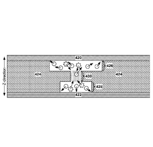
[0086] In Figure 4A, a fluid sample with a mixture of round cells and star
cells is
entrained in the first passage 426, the third passage 428, and the second
passage
430; the fluid flow direction is normal to the page. As can be seen, the
widths of the
first passage 426 and the third passage 428 are both wider than the width of
the
second passage 430. While each passage is shown as having substantially the
same
thickness, e.g., 1/3 of the total thickness of electrically-insulating layer
424, the
passages may also have differing thicknesses. The passages may form a
continuous
fluid flow region between a first electrode layer 420 and a second electrode
layer
422.
[0087] In Figure 4B, an AC voltage has been applied across the first electrode
layer
420 and the second electrode layer 422, producing an electromagnetic field
(shaded
area) concentrated near the second passage 430. In this implementation, the
frequency of the electromagnetic field is such that star cells are attracted
to the field
by DEP, and round cells are repelled from the field by DEP. Arrows are
provided to
indicate the general migration direction of the cells. It is to be understood
that the
electromagnetic field may be present in Figure 4A and 4C as well, although it
is not
shown¨due to the structure of the cell sorter shown in Figures 4A through 4D,
the
fluid sample may be subject to DEP throughout substantially the entire DEP
sorting
region.
[0088] It is to be understood that while the electrode layers shown in Figures
4A
through 4C are shown as being in direct contact with the fluid in the first
and third
passages 426 and 428, the electrode layers 420 and 422 may also have a thin,
electrically-insulating, i.e., non-conducting, coating that separates the
electrode
layers 420 and 422 from the fluid sample. If the coating is thin enough, e.g.,
on the
order of approximately 2 p.m or less, the AC voltage frequency used may be
high
enough that the thin layer does not block electromagnetic field penetration
into the
liquid sample in a manner that substantially impacts the electromagnetic field
pattern within the liquid sample. This may allow the electrode layers 420 and
422 to
be coated with electrically-insulating materials that may prevent (or, if
desired,
encourage) cell or particle adhesion to the electrode layers.
CA 02868261 2014-09-23
WO 2013/148865
PCT/US2013/034145
19
[0089] In Figure 4C, the fluid sample has been exposed to the electromagnetic
field
for a sufficiently long enough period of time that DEP-induced migration of
the star
cells to the second passage 430 has occurred, and DEP-induced migration of the
round cells to the first passage 426 and the third passage 428 has occurred.
[0090] In Figure 4D, the fluid sample is split into two streams by diverting
the first
passage 426 and the third passage 428 from the second passage 430. The first
passage 426 and the third passage 428 are shown using hidden lines since they
branch away from the second passage 430 within the electrically-insulating
layer
424. This causes the star cells concentrated in the second passage to be
physically
separated from the round cells in the first passage 426 and the third passage
428.
[0091] Figure 4E depicts an analysis plot showing the electromagnetic field
strength
through a cross-section of a three-dimensional DEP cell sorter. In Figure 4E,
darker
shading indicates increasing electromagnetic field strength, whereas lighter
shading
indicates the opposite. As can be seen, electromagnetic field strength is
biased
towards the center elevation in the z-direction of the three-dimensional DEP
cell
sorter.
[0092] In two-dimensional cell sorters, the electromagnetic field intensity is
governed by the shape of the electrodes¨in order to generate the desired
electromagnetic field shape, the electrodes must be suitably patterned. By
contrast,
the electromagnetic field intensity in a three-dimensional DEP cell sorter
such as that
depicted in Figures 3A through 3D is governed by the relative widths of the
first
passage, the third passage, and the second passage. This allows the
electromagnetic
field intensity, and thus the DEP effect on the entrained cells, to be
decoupled from
the shape of the electrodes, allowing the electrode layers to simply be flat,
non-
patterned electrodes. Of course, a patterned electrode may still be used if
desired,
although this may change the electromagnetic field strength, and thus the
performance of the cell sorter, in some cases. In some implementations, an
array of
cell sorters may be provided in a common electrically-insulating layer, each
with an
individual planar electrode that may be electrically isolated from the planar
electrodes of the other cell sorters, yet still located on a common
substrate¨in such
CA 02868261 2014-09-23
WO 2013/148865
PCT/US2013/034145
cases, of course, some layer-level electrode patterning may exist to allow
voltages to
each cell sorter to be applied in isolation, but the electrodes at the
individual cell
sorter level may be "unpatterned." In many implementations, the electrodes may
extend along the entire length of the passages within the DEP-separation
region. In
5 other implementations, however, the electrodes may stop prior to the
divergence of
the second passage from the first passage and the third passage¨in such
implementations, however, the concentrated cells may begin to migrate out of
the
second passage due to the absence of the electromagnetic field in the
electrode-less
region of the DEP-separation region, thus reducing cell sorting performance.
While a
10 three-dimensional DEP cell sorter may be implemented with a uniform
electrode in
the DEP separation region, some implementations of such a cell sorter may
utilize
patterned electrodes in the DEP separation region.
[0093] Because the electrodes may remain relatively uniform along the entire
length
of the second passage 330 within the DEP separation region 332, the
15 electromagnetic field generated within the sample fluid may also be
relatively
constant along this same length. This causes the DEP forces generated by such
a
field to act continuously on cells flowing down the first passage 326, the
third
passage 328, and the second passage 330 throughout the entire DEP separation
region 332, regardless of the flow rate of the fluid sample. In effect, the
only major
20 restrictions on fluid flow rate with respect to sorting effectiveness is
that the flow
rate must be low enough that cells in the first channel 326 and the second
channel
328 are exposed to DEP forces for a long enough time period to allow them to
move
from the first channel 326 and the second channel 328 and into the sorting
channel
330, and that the flow rate be low enough that the shear stress experienced by
cells
in the flow be survivable, e.g., on the order of 10 m/sec.
[0094] Because the DEP cell sorter discussed above is largely insensitive to
sample
flow rate, active control of sample flow rate is not necessary as it is with
existing
two-dimensional DEP cell sorters. In fact, a three-dimensional DEP cell sorter
may
even be manually driven, e.g., using a hand-activated squeeze bulb or bellows
to
drive fluid flow through the sorter. This may eliminate the need for a bulky
pump
with precise pressure control in many microfluidic systems. Using three-
dimensional
CA 02868261 2014-09-23
WO 2013/148865
PCT/US2013/034145
21
DEP cell sorters in a large-scale array may allow, for example, a 2cm wide
chip that
could support 100 separate 100 micron-wide sorters, be hand-powered, and
achieve
ml/min of throughput.
[0095] While the above discussion has focused on a three-dimensional DEP cell
5 sorter that focuses positive DEP cells into the second passage, other
passage
configurations may be used as well. For example, if the second passage has a
larger
width than the first passage and the third passage, e.g., forming a "+" cross-
section,
then the resulting electromagnetic field that is generated may be concentrated
in
the first and third passages rather than the second passage. This may cause
cells
10 with negative DEP to congregate in the second passage and cells with
positive DEP to
congregate in the first passage and the third passage. A three-dimensional DEP
cell
sorter with such a cross-section may be used to collect negative DEP cells.
[0096] Generally speaking, three-dimensional DEP cell sorters function by
sorting
cells primarily in the "z" direction, i.e., normal to the overall plane of the
electrode
layers and the electrically-insulating layer. This may be accomplished by
customizing
the electromagnetic field that drives DEP movement of cells to vary as a
function of
z-direction position with respect to the electrode layers. Such
electromagnetic field
customization may be accomplished by varying the cross-section of the passages
through which sample fluid flows and within which the electromagnetic field is
generated. By varying the cross-sectional geometry of these passages in the z-
direction, some zones of the passage along the z-axis having an
electromagnetic field
concentration may attract target cells having positive DEP, whereas other
zones of
the passage along the z-axis having a dilute electromagnetic field may attract
target
cells having negative DEP. In three-dimensional cell sorters, migration of
cells in a
direction transverse to the fluid flow direction is decoupled from the fluid
flow rate
and is instead driven by forces produced by DEP effects. Thus, in both zero-
flow and
high-flow situations, the DEP effect is capable of migrating the cells in the
z-direction
and into the collection region.
[0097] By contrast, two-dimensional DEP cell sorters function by sorting cells
in the
"y" direction, L e., transverse to the fluid flow direction (the "x"
direction) and
CA 02868261 2014-09-23
WO 2013/148865
PCT/US2013/034145
22
parallel to the overall plane of the electrode layers and the electrically-
insulating
layer. In such two-dimensional DEP cell sorters, the electromagnetic field is
customized by patterning the electrodes on the electrode layers so that the
electromagnetic fields produced have a pattern in the x-y plane that is at an
angle to
the fluid-flow direction. The combination of forces provided by the fluid flow
and
the DEP effect in a two-dimensional DEP cell sorter cause the cells to migrate
in the
y-direction¨if the cells migrate in the y-direction far enough, then they may
be
shunted into a collection channel. This transverse movement, however, is
directly
linked to the fluid flow speed¨if there is no fluid flow, then the cells will
not migrate
(aside from some small movement towards the electrodes). If there is too much
fluid flow, the fluid flow forces will overcome the DEP forces and the cell
may be
pushed out of the DEP effect area and not migrate far enough to be in the
collection
channel by the time the fluid sample reaches the waste and collection
channels.
[0098] In practice, three-dimensional cell sorters may improve on two-
dimensional
cell sorters by two to three orders of magnitude or more with respect to
throughput,
putting them on par with other technologies, such as inertial cell sorters. In
contrast
to such other technologies, however, the three-dimensional cell sorter may be
packaged in a much smaller volume.
[0099] It is to be understood that while the three-dimensional DEP cell
sorters
discussed above feature a set of three passages in a sideways-"H"
configuration,
other three-dimensional DEP cell sorters may feature other cross sections and
numbers of passages. For example, a two-passage DEP cell sorter may be made
where one of the passages is of a different width than the other passage.
Greater
numbers of passages are also possible. For example, 7 passages may be provided
in
a three-dimensional DEP cell sorter¨each odd-numbered passage may be wider
than the even-numbered passages, resulting in a concentrated electromagnetic
field
in each even-numbered passage. Cells or particulates may thus migrate from the
odd-numbered passages into the even-numbered passages in the DEP-separation
region when the electromagnetic field is present. Each even-numbered passage
may
diverge from the odd-numbered passages in the post-DEP separation region. In
some such implementations, each even-numbered passage may be routed to a
CA 02868261 2014-09-23
WO 2013/148865
PCT/US2013/034145
23
different location¨in the example given, this may allow for three separate
batches
of cells to be extraction from a common sample while allowing for three
different
post-extraction analyses to be performed on the extracted cells.
[0100] In some implementations, the cross-sectional variation in the z-
direction of
the passages may be provided dynamically. For example, a fluid passage for
sample
fluid flow may be provided, e.g., a rectangular cross-section passage. The
fluid
passage may have a floor and a ceiling provided by electrode layers. Two
parallel
passages may be located next to the fluid passage, one on either side. The
parallel
passages may be separated from the fluid passage by a thin, deformable wall.
If the
parallel passages are pressurized, e.g., with a gas or a liquid, the pressure
may cause
the deformable walls to distend into the fluid passage, causing a narrowing in
the
cross section of the fluid passage commensurate with the degree of deflection
in the
thin walls. An electromagnetic field produced by applying a voltage across the
electrode layers may concentrate at the narrowing point, and positive DEP
particulates or cells may then gather at that location. Conversely, if a
vacuum is
drawn on the parallel passages, this may cause the deformable walls to distend
into
the parallel passages, causing the fluid passage to bulge outwards. This may
cause
cells with a negative DEP to concentrate near the point of maximum bulge
deflection.
[0101] Figures 5A through 5C depict cross-sectional views of a microfluidic
cell sorter
structure having a dynamically-variable passage cross-section. As can be seen,
an
electrically-insulating layer 524 may be sandwiched between a first electrode
layer
520 and a second electrode layer 522. A fluid flow passage 542 may be bounded
by
the first electrode layer 520 along an upper side and the second electrode
layer 522
.. along a lower side; it is to be understood that the terms "upper" and
"lower" are
used to refer to the orientation of such boundaries with respect to the
Figure, and
may not be reflective of the actual orientation of such boundaries in an
actual
implementations.
[0102] The fluid flow passage 542 may also be bounded by thin walls 540, which
may
separate the fluid flow passage 542 from side passages 538 that may be
configured
CA 02868261 2014-09-23
WO 2013/148865
PCT/US2013/034145
24
to run substantially parallel to the fluid flow passage 542. The thin walls
540 may
have a substantially uniform thickness with respect to the distance between
the fluid
flow passage 542 and the side passages 538. The side passages 538 may be
configured to be fluidly isolated from the fluid flow passage 542. Actuation
ports
536 may be provided and may be in fluid communication with the side passages
538.
The actuation ports 536 may be used to provide a pressure differential between
the
fluid flow passage 542 and the side passages 538. Depending on the nature of
the
pressure differential, the thin walls 540 may distend into the fluid flow
passage 542,
as is shown in Figure 5B for a greater pressure in the side passage 538, or
into the
side passages 538, as is shown in Figure 5C for a lesser pressure in the side
passage
538. Dashed lines show the location of the thin walls 540 prior to deflection.
[0103] When an AC voltage is applied between the first electrode layer 520 and
the
second electrode layer 522, a DEP effect may be generated within a fluid
pumped
through the fluid passage 542. In Figure A, the cross-section of the fluid
passage 542
may be relatively constant, and there may be little to no concentration of
cells, e.g.,
of round cells and star cells, in any one region of the fluid passage 542 due
to the
DEP effect. However, if the thin walls 540 are distended into the fluid
passage 542
by a positive pressure differential between the side passages 538 and the
fluid
passage 542, then this may cause the electromagnetic field generated within
the
fluid to be concentrated on or biased towards the narrowest portion of the
cross
section of the fluid passage 542, e.g., the center of the fluid passage 542 in
this
example. In this case, the star cells are positive DEP cells at the frequency
used for
the AC voltage and are attracted to the center of the fluid passage 542 where
the
DEP effect is the most pronounced.
[0104] If the thin walls 540 are instead distended into the side passages 538,
the
electromagnetic field may be weakest at or biased away from the center of the
fluid
passage 542. This may cause negative DEP cells at the frequency used to
migrate
towards the center of the fluid passage 542.
[0105] This dynamic structure may allow for a single structure to be used to
sort
cells or particulates exhibiting both negative and positive DEP, depending on
how
CA 02868261 2014-09-23
WO 2013/148865
PCT/US2013/034145
the thin walls are deformed. Such a DEP sorting structure may be used in an
implementation similar to that shown in Figures 3A through 3D in the DEP
sorting
region 332 to segregate desired cells from a larger sample.
[0106] It is to be understood that the thin walls may be deformed dynamically,
e.g.,
5 transitioned from an un-deformed state to a deformed state or from one
deformed
state to another as needed, or may be deformed permanently as part of a
manufacturing process. For example, it may be desirable in some instances to
fabricate the electrically-insulating layer of a three-dimensional DEP cell
sorter in a
single layer fabrication process, as opposed to multiple layers requiring
alignment
10 with one another. In such cases, a structure similar to that shown in
Figures 5A
through 5C may be used, except that the side passages 538 and the actuation
ports
536 may instead extend all the way to the first electrode layer 520 and the
second
electrode layer 522 in the z-direction. After the electrically-insulating
layer has been
sandwiched between the electrode layers, PDMS gel or other substance may be
15 flowed into the side passages 538 to displace air or gas. The PDMS gel
or other
substance may then be pressurized to distend the thin walls 540 into the fluid
passage 542 or partially suctioned out to distend the thin walls 540 into the
side
passages 538. Once the fluid passage 538 reaches the desired cross-section,
the
PDMS gel or other substance may be sealed off to prevent alteration of the
thin wall
20 distension, or may even be cured so as to solidify and form
substantially rigid
structure. Such techniques may also be practiced with other dynamically-
variable
structures that are not capable of being manufactured as a single-layer
electrically-
insulating layer.
[0107] It is to be understood that, in some implementations, complete physical
25 separation of desired cells from the fluid sample via a collection
passage may not be
desired, e.g., in some implementations, merely separating the desired cells
from
other cells in the fluid sample in the z-direction, i.e., in a direction
orthogonal to the
overall plane of the cell sorter microfluidic structure, may be sufficient.
For example,
Figures 6B-6D depict images captured through a microscope of a DEP sorting
region
of a prototype three-dimensional DEP cell sorting structure with a sample
fluid
flowing through it from the top of the page to bottom of the page; the three-
CA 02868261 2014-09-23
WO 2013/148865 PCT/US2013/034145
26
dimensional cell sorting structure is shown in overview in Figure 6A. For
clarity, each
image in Figures 6B through 6C is reproduced twice, with the original image on
the
left and a contrast-enhanced image on the right. The contrast-enhanced images
have only been contrast-enhanced within the dashed rectangle or rectangles on
each
image. Figure 6A through 6D's perspectives are plan view, i.e., the viewing
directions are normal to the overall plane of the microfluidic structure. The
portion
that is shown in Figures 6B through 6C may, for example, correspond to the DEP
separation region 332 from Figures 3A through 3D. The microscope used to
capture
the images for Figures 6B through 6D is focused on a focal plane corresponding
to a
passage that, for example, corresponds to the second passage 330 of Figures 3A
through 3D or the second passage 430 of Figures 4A through 4C. Cells that are
in
passages above or below the passage in the focal plane will be out of focus,
whereas
cells that are within the passage in the focal plane will be in-focus (or at
least more
in-focus).
[0108] In Figure 6B, the AC voltage that provides the DEP effect has not been
applied. A dashed rectangle outlines an area where an "unfocused" cell is
barely
visible and is not in sharp focus. This cell is slightly more visible in the
contrast-
enhanced region of the right-hand image.
[0109] In Figure 6C, the AC voltage that provide the DEP effect has been
applied to
electrode layers on top of and beneath the three-dimensional DEP cell sorting
structure. The electrode layers may, for example, be ITO-coated glass so as to
be
substantially optically transparent to facilitate, in this case, imaging of
the behavior
of cells within the cell sorting structure. Such optically-transparent
electrode layers
may allow for optically-based analysis techniques to be used to analyze cells
or other
materials that may be concentrated within DEP concentration zones of a three-
dimensional cell sorter or particulate sorter. As can be seen in Figure 6C,
the
application of AC voltage to the electrode layers has caused the first cell
visible in
Figure 6B to migrate in the z-direction and into the passage corresponding
with the
focal plane. A second cell, further upstream from the first cell, is also
barely visible
in the passage in Figure 6C.
CA 02868261 2014-09-23
WO 2013/148865
PCT/US2013/034145
27
[0110] In Figure 6D, the DEP effect caused by the application of AC voltage
across
the electrode layers has caused both the first cell and the second cell to
move into
the passage corresponding with the focal plane, allowing for sharp imaging of
both
cells. In some implementations, a combination of such z-separation and proper
focal
plane alignment may allow for target cells to be separated from a fluid sample
within
a DEP separation region and optically processed, e.g., counted using a machine
vision system, without actually mechanically separating the collection stream
from
the waste stream of the three-dimensional DEP cell sorter. In other
implementations, however, actual separation of the sorted cells from the waste
stream in the post-DEP separation region may still occur, allowing such
separated
cells to be routed to subsequent chambers for analysis where the presence of
other
cell material may be undesirable.
[0111] Three-dimensional DEP cell sorters such as those discussed herein may
exhibit performance that is a significant improvement over "tilted electrode"
DEP
cell sorters such as those depicted in Figures 1 and 2. For example, tilted
electrode
designs typically feature DEP interaction distances that are limited to the
length of
the electrode patterns, which are typically limited to several hundred m in
length,
whereas three-dimensional DEP cell sorters such as those described herein may
have
DEP interaction distances that span across an entire microfluidic chip
(currently,
microfluidic chips have a typical size of 10cm by 10cm), and thus may have DEP
interaction distances of 10 cm or longer, which is 3 orders of magnitude
greater than
the fastest tilted-electrode DEP sorters currently available.
[0112] Due to the dependence of the three-dimensional DEP sorting effect on
fluid
passage cross-section geometry, DEP sorting due to a particular cross-
sectional
passage shape may occur along such a passage or passages for as long as the
cross-
sectional passage shape exists. Thus, three-dimensional DEP sorting may occur
in a
passage or passages across the entire span of a microfluidic chip, e.g.,
approximately
10cm (for a passage parallel to the chip edge) or 14 cm (for a passage on the
chip
diagonal) on a 10cm-square chip. Moreover, three-dimensional DEP sorting
structures may also be implemented in non-linear patterns, e.g., the passages
in
which three-dimensional DEP sorting occurs may be routed to as to turn corners
or
CA 02868261 2014-09-23
WO 2013/148865
PCT/US2013/034145
28
loop back on themselves (similar to the U-turn shown in Figure 9(d)) to form a
serpentine passage. Using such non-linear patterns, a passage for a three-
dimensional DEP cell sorter on a 10cm-square microfluidic chip may reach up to
1m
to 10m in length.
[0113] While various materials may be used for the electrically-insulating
layer, one
common material used in microfluidic devices is PDMS. PDMS is an optically
clear,
elastomeric material that can be flowed onto a mold, cured, and then removed.
PDMS is particularly well-suited to reproducing small-scale, e.g., nano- or
micro-
scale, features such as microfluidic channels, ports, etc. Currently, existing
manufacturing methods for PDMS structures focus on forming individual PDMS
layers including various microfluidic features and then bonding them to each
other
to produce a multi-layer stack, each layer having a different set of features.
Such
techniques allow for multiple separate fluid flow passages to exist within a
single
multi-layer PDMS stack. However, current production techniques typically have
issues reliably producing through-layer vias to allow passages on different
layers to
fluidly communicate with one another. Specifically, the present inventors have
realized that current production techniques may produce edge ridges around
such
vias. In the context of a large, linear or curvilinear via, e.g., such as that
formed by
the second passage 330 between the first passage 326 and the third passage
328,
such ridges may interfere with inter-layer bonding and may also cause
undesirable
interference with the generation of the electromagnetic field within the
sample
fluid. Since many PDMS structures are manufactured using a multi-layered
approach, such edge ridges may appear on multiple layers and, in aggregate,
result
in large non-uniformities in the overall thickness of the PDMS structure,
which is
generally undesirable. Other materials that may be suitable for use in the
electrically-insulating layer may include silicon dioxide, silicon nitride,
and
amorphous, poly-, and single-crystalline silicon, as well as other
electrically-
insulating materials. Thus, while PDMS may be well-suited for forming three-
dimensional DEP cell sorter electrically-insulating layers, other materials
may also be
used.
CA 02868261 2014-09-23
WO 2013/148865 PCT/US2013/034145
29
[0114] Given the suitability of PDMS for producing the above-discussed three-
dimensional DEP cell sorter structures, the present inventors conceived of a
new
manufacturing technique for multi-layer PDMS structures that allows for
through-via
features with reduced, or eliminated, edge-ridges. This technique may be used
to
produce cell sorters as detailed herein, but may also be used to produce any
number
of other PDMS multi-layer structures. It may be especially useful in producing
multi-
layer PDMS structures requiring through-via structures. The technique may also
be
used, with appropriate modification, to produce layer structures from
elastomeric
materials other than PDMS.
[0115] It is to be understood that three-dimensional DEP cell sorters as
discussed
herein may also be made using techniques other than those discussed in detail
herein. For example, a three-dimensional DEP cell sorter may be made using
plastic
molding to create channel or passage structures and laser drilling to create
interlayer
vias, e.g., to join the passages together in the z-direction within the DEP
separation
region.
[0116] Figures 5A through 5ZB depict, via simplified cross-sectional views,
various
stages of a manufacturing technique for producing multi-layer PDMS structures.
The
structure that is being constructed in Figures 5A through 5ZB is a portion of
a three-
dimensional DEP cell sorter, e.g., the features within the DEP separation
region of
such a cell sorter. Figures 5A through 5ZB are not drawn to scale. In Figures
5A
through 5P, the Figures depict two different manufacturing streams¨the steps
in
the streams may be largely the same, but the molds used may have different
feature
sizes. For example, the cross-sections on the left side of each Figure depict
the
formation of a PDMS layer that may be used to provide the first passage or the
third
passage of a cell sorter, and the cross-sections on the right side of each
Figure may
depict the formation of a PDMS layer that may be used to provide the second
passage of the cell sorter. Figures 50. through 5ZB depict the assembly of the
layers
into an assembled cell sorter.
[0117] In Figure 7A, a hard substrate may be prepared for etching by
depositing or
providing a photo-patternable or photo-resistive material on the substrate,
such a
CA 02868261 2014-09-23
WO 2013/148865
PCT/US2013/034145
material may be, for example, negative photoresist SU8 or positive photoresist
4Z4620, and the substrate may, for example, be silicon or glass, although
other
photoresists or photo-patternable materials may be used as well, as well as
other
substrate materials. In Figure 7B, an etching operation may remove material
from
5 the hard substrate to form a hard master mold. Alternatively, the raised
features on
the hard master molds may be formed by deposition instead of etching. In
Figure
7C, the hard master mold is coated with a conformal silane surface treatment
to
facilitate later removal of cured PDMS from the hard master mold. In Figure
7D,
uncured PDMS may be poured onto the hard master mold and cured to form a
10 complementary PDMS mold. In Figure 7E, the PDMS mold may then be
separated
from the hard master mold. In Figure 7F, the PDMS mold may be coated with a
conformal silane surface treatment.
[0118] In Figure 7G, the PDMS mold may be temporarily set aside and another
hard
substrate, e.g., silicon or glass, may be prepared by pouring uncured PDMS
onto the
15 hard substrate. In Figure 7H, the PDMS mold may be retrieved, and in
Figure 71, the
PDMS mold may be pressed into the uncured PDMS on the substrate and the
uncured PDMS may then be cured. In Figure 7J, the PDMS mold may be removed
from the cured PDMS on the substrate. The resulting PDMS structure on the
substrate may be an exact, or near-exact, duplicate of the hard master mold
and
20 may be referred to herein as the PDMS master mold. In some
implementations of
the method, the PDMS master mold fabrication may be skipped, and the hard
master mold may be used in place of the PDMS master mold in the steps below. A
hard master mold may be more suited to large-scale production runs since such
master molds are more robust than PDMS master molds. A PDMS master mold may
25 be used for low-scale production runs or for laboratory testing where
higher feature
quality may be desired.
[0119] In Figure 7K, the PDMS master mold may be coated with a CYTOPTm surface
treatment to assist in later removal of cast PDMS parts.
[0120] In Figure 7L, uncured PDMS may be applied to the PDMS master mold. In
30 Figure 7M, a hybrid stamping is used to compress the uncured PDMS
against the
CA 02868261 2014-09-23
WO 2013/148865
PCT/US2013/034145
31
PDMS master mold. A hybrid stamping may include a plate of material with a
much
higher modulus than PDMS, e.g., is much stiffer than PDMS; the plate may have
a
thin layer of PDMS on at least one side. For example, the plate may have a
plastic
plate with a Young's modulus of 3.2 GPa and be covered with a 301im layer of
PDMS
(Young's modulus of 0.0006 GPa) on one side. The plate may be located such
that a
very thin layer of PDMS exists between the plate and the uncured PDMS and the
PDMS master mold. This thin layer may be, for example, on the order of 500
microns or less in thickness. In practice, thicknesses of 10 to 30 microns
have been
found to work well. The plate may be plastic, glass, or other material with a
substantially higher modulus than that of PDMS. In practice, plastic plates
proved to
be more robust than glass plates. The plate may act as an intermediate load
spreader within the PDMS stamping to distribute a compression load across the
PDMS master mold and the uncured PDMS. The thin layer of PDMS may allow for
very small localized deflections that allow for full contact between the PDMS
mold
and the stamping, thus ensuring clear via formation, while avoiding the
creation of
large edge ridges that appear when a non-hybrid stamping is used.
[0121] The embedded-plate stamping shown may be provided by spin-coating the
plate with PDMS. However, it was discovered that PDMS exhibits inconsistent
curing
behavior when applied in too thin a layer¨the PDMS will frequently not set at
thicknesses such as those discussed above and remains in a liquid state,
resulting in
an unreliable manufacturing technique. It was a surprising discovery, however,
to
learn that adding a platinum catalyst to the PDMS can cause a thin PDMS layer
to set
reliably regardless of thickness. While catalysts have been used to accelerate
cure
rate it is believed that such catalysts have not been used to reverse a non-
cure or
inconsistent cure situation. Thus, the technique may include preparing a
stamping
(this step is not shown) by coating a substantially rigid plate with a thin
layer of
PDMS with a platinum catalyst added. The stamping may also have a thicker
layer of
PDMS on the opposite side of the plate to allow for easy handling or
integration with
existing equipment, although such a thicker layer is not strictly necessary.
The thin
layer of PDMS (or the entire PDMS stamping) may be treated with a silane
surface
treatment, e.g., trichloro (1H,1H,2H,2H-perfluorooctyl) silane (also referred
to as
CA 02868261 2014-09-23
WO 2013/148865
PCT/US2013/034145
32
"PFOCTS"). Such PFOCTS treatment may be carried out via an evaporation process
within a closed chamber.
[0122] The platinum catalyst may, for example, be platinum-
divinyltetramethyldisiloxane (C81-1180PtSi2), which is typically used as in
ingredient in
hard PDMS (the PDMS discussed herein is soft PDMS, and remains soft PDMS even
after the platinum catalyst is added). The platinum catalyst may be added in
addition to any normally-applied curing agent, although the amount of platinum
catalyst that may be applied may be very slight. For example, in some
implementations, between 16 to 20 pi of platinum-divinyltetramethyldisiloxane
(C8F1180PtSi2) may be added per 10g of PDMS base and 1g of PDMS curing agent.
Of
course, in the future, manufacturers may begin adding such a catalyst to
existing
curing agents to eliminate the need to add the catalyst separately, so it is
to be
understood that the above ratio is with reference to standard PDMS curing
agents in
existence at the time of this filing. A later-offered curing agent that has a
composition similar to existing curing agents and also having a platinum-
divinyltetramethyldisiloxane (C8H18OPtSi2) present in approximately the same
ratio.
For example, a curing agent has a mass fraction of platinum-
divinyltetramethyldisiloxane of approximately 1% to 2.5%, then this would be
substantially equivalent to the separately-added catalyst described above.
[0123] In some implementations, if a PDMS master mold is used, the hybrid
stamping may be replaced by a hard stamping, e.g., a plate of glass or hard
plastic.
In such implementations, the PDMS master mold may deflect slightly to allow
for a
tight mechanical interface between the PDMS master mold and the stamping, thus
allowing the creation of clean vias.
[0124] In Figure 7N, the stamping has been compressed against the uncured PDMS
and the PDMS master mold and the uncured PDMS then cured. In Figure 70, the
cured PDMS layer is removed from the PDMS master mold by pulling the stamping
away from the PDMS master mold. Due to the higher bond strength in silane-
treated surfaces as compared with CYTOP-treated surfaces, the PDMS layer will
stay
bonded to the stamping, allowing for easy transfer to other structures.
CA 02868261 2014-09-23
WO 2013/148865
PCT/US2013/034145
33
[0125] Figure 7P depicts the removed PDMS layer bonded to the stamping; the
PDMS layer may be treated with an oxygen plasma to facilitate later bonding
with a
glass or PDMS structure. In Figure 70, one of the PDMS layers is positioned
over a
prepared glass substrate; the glass substrate may, for example, be prepared by
coating it with an electrically-conductive coating such as ITO so that it may
act as an
electrode layer of a DEP cell sorter. In Figure 7R, the PDMS layer may be
directly
bonded to the glass substrate as a result of the oxygen plasma treatment of
the
PDMS layer. In Figure 7S, the stamping may be removed¨due to the higher bond
strength of the direct bonding via oxygen plasma treatment as compared with
the
bond across the silane-treated surfaces, the PDMS layer may separate from the
stamping and remain cleanly attached to the glass substrate. The PDMS layer
placed
on the substrate in this case corresponds to a sublayer of an electrically-
insulating
layer in a DEP cell sorter having a first or third passage in it.
[0126] In Figure 7T, another PDMS layer, this time corresponding with a
sublayer of
an electrically-insulating layer in a DEP cell sorter having a second passage
in it, may
be positioned over the previously-placed PDMS layer using the stamping to
which it
is attached. This second PDMS layer may also be treated with an oxygen plasma
to
facilitate direct covalent bonding to the previously-placed PDMS layer. In
Figure 7U,
the second PDMS layer may be directly bonded to the first PDMS layer by
compressing it into the first PDMS layer with the stamping. In Figure 7V, the
stamping may be removed in much the same manner as in Figure 7S.
[0127] In Figure 7W, a third PDMS layer, in this case similar to the first
PDMS layer,
may be positioned over the first and second PDMS layers. The third PDMS layer,
as
with the other PDMS layers, may be treated with an oxygen plasma. In Figure
7X,
the third PDMS layer may be directly bonded to the second PDMS layer to form a
three-layer stack of PDMS layers that are fused into one, essentially
contiguous,
structure. In Figure 7Y, the stamping may be removed, leaving the 3-layer PDMS
structure behind. In Figure 7Z, the exposed top of the PDMS structure may be
prepared for bonding to another hard substrate, e.g., glass. In Figure 7ZA,
the hard
substrate may be positioned over the assembled PDMS stack, and in Figure 7ZB,
the
hard substrate may be bonded to the stack.
CA 02868261 2014-09-23
WO 2013/148865
PCT/US2013/034145
34
[0128] For each PDMS layer that is bonded using direct bonding via oxygen
plasma
treatment, the direct covalent bonds formed at the oxygen plasma-treated
surface
may be substantially stronger than the bond between the hybrid stamping and
the
PDMS layer, allowing the hybrid stamping to be removed from the PDMS layer and
re-used after the PDMS layer is bonded at the oxygen plasma-treated surface.
[0129] Figure 8 depicts a flow chart summarizing the above technique at a high
level.
In block 802, the technique may begin. In block 804, uncured PDMS gel may be
poured or deposited onto a mold. In block 806, the uncured PDMS gel may be
pressed into the mold using a hybrid stamping. It is to be understood that if
a PDMS
mold is used, the hybrid stamping may be replaced with a hard stamping, e.g.,
a flat
plastic plate. In block 808, the compressed uncured PDMS gel may be cured.
After
curing, the resulting cured PDMS layer may be demolded from the mold in block
810
using the stamping. In block 812, the cured PDMS layer may be transferred to a
receiving surface, e.g., a glass or plastic substrate or a previously-applied
PDMS
layer, and bonded to the receiving surface. In block 814, the PDMS layer may
be
released from the stamping and the stamping may then be re-used in another
molding process. In block 816, a decision may be made as to whether further
PDMS
layers are desired. If so, then the technique may return to block 804
(although
different molds may be used as needed). In not, then the technique may proceed
to
block 818. It is to be understood that the above technique may be augmented by
additional activities (not shown) that may be interspersed between various
activities
shown in Figure 8. Additionally, other activities may precede or follow blocks
802
and 818, i.e., the technique is not limited to only the activities listed.
[0130] The resulting structure from techniques such as those outlined above
with
respect to Figures 7A through 7ZB and Figure 8 may provide very clean inter-
layer via
features, and may thus be particularly well-suited for microfluidic devices
feature
such vias, e.g., a DEP cell sorter as discussed above with respect to Figures
3A
through 3D. The above technique may be modified as needed to omit certain
steps,
add other steps, and otherwise tailor the technique for particular design
requirements. For example, it may be possible to form features with stepped
cross-
sections in the molds, thus reducing the number of individual layers that must
be
CA 02868261 2014-09-23
WO 2013/148865
PCT/US2013/034145
made and bonded together. While the depicted technique was shown for a 3-layer
stack of PDMS layers, more or less PDMS layers may be manufacturing in this
manner and assembled into a PDMS layer stack. This manufacturing technique may
be used for a variety of other PDMS structures besides three-dimensional DEP
cell
5 sorter structures, e.g., microfluidic structures having high aspect-ratio
features.
[0131] Figure 9 depicts two examples of molded microfluidic features and the
edge
ridges, or lack thereof, formed using two different manufacturing processes.
In the
upper half of Figure 9, an image of a channel or passage produced using a non-
hybrid
stamping, i.e., a large-thickness, solid PDMS stamping, is on the right (b),
and a plot
10 of the edge profile at the circled location in (b) is shown on the left
in (a). As can be
seen, there is a 601..tm edge ridge present.
[0132] In the lower half of Figure 9, an image of a channel or passage made
using a
hybrid stamping, as discussed herein, is shown on the right (d), and a plot of
the
edge profile at the circled location in (d) is shown on the left in (c). As
can be seen,
15 there is no discernible edge ridge present.
[0133] It is to be understood that while the discussion herein of three-
dimensional
DEP cell sorter structures has focused primarily on structures where the
electrically-
insulating layer is sandwiched between discrete electrode layers, in some
implementations of three-dimensional DEP cell sorters, portions of the
electrically-
20 insulating layer may be formed directly on the electrode layers. For
example, in
some implementations, sub-layers of the electrically-insulating layer may be
formed
by materials deposited directly on the electrode layers using a patterned
deposition
or removed from an electrically-insulating layer deposited on the electrode
layers
using an etching technique. The patterning may include passages that partially
form
25 a three-dimensional DEP cell sorter. Another sub-layer of electrically-
insulating
material, e.g., a PDMS sub-layer, may then be sandwiched between the electrode
layers with the patterned, electrically-insulating sub-layers. The aggregate
electrically-insulating structure may thus include the PDMS sub-layer, as well
as the
electrically-insulating sub-layers formed directly on the electrode layers.
Electrically-
CA 02868261 2014-09-23
WO 2013/148865
PCT/US2013/034145
36
insulating sub-layers that are formed directly on the electrode layers may,
for
example, be more than 2 m thick.
[0134] While various implementations have been described herein, it should be
understood that they have been presented by way of example only, and not
limitation. Thus, the breadth and scope of the present disclosure should not
be
limited by any of the implementations described herein, but should be defined
only
in accordance with the following and later-submitted claims and their
equivalents.
[0135] It will be understood that unless features in any of the above-
described
implementations are expressly identified as incompatible with one another or
the
surrounding context implies that they are mutually exclusive and not readily
combinable in a complementary and/or supportive sense, the totality of this
disclosure contemplates and envisions that specific features of those
implementations can be selectively combined to provide one or more
comprehensive, but slightly different, technical solutions. It will therefore
be further
appreciated that the above description has been given by way of example only
and
that modifications in detail may be made within the scope of the disclosure.