Note: Descriptions are shown in the official language in which they were submitted.
CA 02868742 2014-09-26
WO 2013/106036
PCT/US2012/032661
IMPEDANCE MATCHING CIRCUIT
THE FIELD OF THE INVENTION
The present invention relates to power transfer. More specifically, the
present
invention relates to optimum power transfer from a power source to a thermal
surgical
instrument.
BACKGROUND
Circuits may be designed with maximum voltage to load, maximum power to load
or, sometimes, no thought to power or voltage transfer. In many situations,
maximum
power transfer is desirable, as it provides maximum power to the load. It is
believed
that maximum power transfer may be achieved by matching the impedance of the
source to the load (and any intermediate lines or components). Circuits may
use a
matching network on the source side and load side (see FIG. 1A) or on one side
only.
In general, impedance has a complex value; this means that loads (symbolized
as
Z) generally have a resistance component (symbolized as R) which forms the
real part
of Z and a reactance component (symbolized as X) which forms the imaginary
part of
Z. Power transfer theory dictates that for maximum power to be transferred,
the
source impedance (Zs) should equal the complex conjugate of the load impedance
(ZL) such that the following equation holds true: Rs+jXs= RL-jXL (see FIG.
1B). As
reactance X is variable with frequency, the matching network is generally
tuned to
one frequency.
Matching the load to the characteristic impedance (Z0) of the transmission
line
allows reflectionless matching, minimizing reflections from the load. Thus, a
transmission line connecting the source and load together would ideally be the
same
impedance: ZL = Zo = Zs.
While in an ideal world, Zs, Z0 and ZL would be immutable and the same for
every
product produced, the impedances may be variable due to tolerances and design
in
CA 02868742 2014-09-26
WO 2013/106036
PCT/US2012/032661
2
manufacturing. Therefore, there is a need to customize each circuit to match
impedances in a cost efficient manner.
SUMMARY OF THE INVENTION
It is an object of the present invention to provide an improved impedance
matching
circuit for a thermal surgical instrument.
According to one aspect of the invention, a conductive layer may be used as a
variable capacitor. The conductive layer may be formed as part of a circuit
board,
flex board, etc. As the system monitors standing wave ratio, portions of the
circuit
board may be removed until a minimum of the standing wave ratio is obtained.
Two
conductive layers may be used to provide adjustments for the series
capacitance and
parallel capacitance. Removing part of a conductive layer from one side of the
circuit board may adjust the series capacitance, while removing part of a
conductive
layer from the other side may adjust the parallel capacitance
According to another aspect of the invention, a surgical tip may contain a
matching
circuit or network. The surgical tip may comprise different geometries having
different characteristic impedance. Additionally, due to variations in
fabrication, any
two similar tips may have slightly different characteristic impedances. Thus
each tip
may be individually configured using the matching circuit. The surgical tips
may be
attachable to a handpiece which receives electrical energy from a power source
via a
transmission line having characteristic impedances that match the impedance of
the
surgical tip to achieve substantially maximum power transfer.
According to another aspect of the invention, standing wave ratio may be
monitored to determine if the system has encountered a failure or a limit.
According to another aspect of the invention, a capacitor and/or inductor,
such as
an electronically controlled capacitor and/or inductor may be used in tuning
the
circuit. In one embodiment, the capacitor and/or inductor value may be set at
manufacturing as part of the impedance matching setting. In another
embodiment, the
matching circuit may contain a processor that monitors SWR and adjusts an
electronically controlled capacitor and/or inductor to minimize SWR.
According to another aspect of the invention, a coaxial cable having a
characteristic impedance may be used in tuning the circuit.
CA 02868742 2014-09-26
WO 2013/106036
PCT/US2012/032661
3
According to still another aspect of the invention, inductors, transformers,
resistors, varactors, coaxial cables, and/or combinations thereof may be used
in tuning
the circuit.
These and other aspects of the present invention are realized in an impedance
matching circuit as shown and described in the following figures and related
description.
BRIEF DESCRIPTION OF THE DRAWINGS
Various embodiments of the present invention are shown and described in
reference to the numbered drawings wherein:
FIG. lA shows a schematic of a circuit with two matching circuits in
accordance
with the prior art;
FIG. 1B shows a schematic of a circuit with a source impedance and load
impedance in accordance with the prior art;
FIG. 2 shows a diagram of a surgical system in accordance with one aspect of
the
present invention;
FIG. 3 shows a schematic of an equivalent circuit with a surgical element;
FIG. 4 shows a chart of standing wave ratio to frequency;
FIG. 5 shows a diagram of an unaltered circuit board matching circuit;
FIG. 6A shows a diagram of a single layer circuit board matching circuit;
FIG. 6B shows a diagram of a two layer circuit board matching circuit;
FIG. 7 shows an equivalent schematic of the circuit board matching circuit in
5B;
FIG. 8A shows an alternate schematic of a circuit board matching circuit;
FIG. 8B shows another alternate schematic of a circuit board matching circuit
with
a varactor;
FIG. 9 shows a replaceable tip matching circuit and joint;
FIG. 10A shows a Smith chart and schematic for matching the load of a surgical
tip with a source impedance using capacitors;
FIG. 10B shows a Smith chart and schematic for matching the load of a surgical
tip with a source impedance using a capacitor and a coaxial cable;
FIG. 10C shows a Smith chart and schematic for matching the load of a surgical
tip with a source impedance using capacitors and an inductor;
CA 02868742 2014-09-26
WO 2013/106036
PCT/US2012/032661
4
FIG. 10D shows a Smith chart and schematic for matching the load of a surgical
tip with a source impedance using a capacitor and transformer;
FIG. 11A shows a perspective view of a thermal surgical tool system;
FIG. 11B shows a perspective view of an alternate embodiment of a thermal
surgical tool system;
FIG. 12 shows a diagram of a thermal surgical tool system;
FIG. 13A shows a thermal surgical tool system with heat prevention terminals,
heat sink, and wireless communication devices;
FIG. 13B shows a thermal surgical tool system with an impedance matching
network;
FIG. 14 shows a close-up, side cross-sectional view of a single layer
ferromagnetic
coated conductor tip in accordance with one aspect of the present invention;
FIG. 15 shows a close-up, side cross-sectional view of a single layer
ferromagnetic
coated conductor tip with a thermal insulator in accordance with one aspect of
the
present invention;
FIG. 16A shows a close-up view of ferromagnetic coated conductor surgical tool
tip with a loop geometry in accordance with one aspect of the present
invention;
FIG. 16B shows a close-up view of a ferromagnetic coated conductor surgical
tool
tip with a generally square geometry in accordance with one aspect of the
present
invention;
FIG. 16C shows a close-up view of a ferromagnetic coated conductor surgical
tool
tip with a pointed geometry;
FIG. 16D shows a close-up view of a ferromagnetic coated conductor surgical
tool
tip with an asymmetrical loop geometry;
FIG. 16E shows a close-up view of a ferromagnetic coated conductor surgical
tool
tip with a hook geometry in which the concave portion may be used for
therapeutic
effect, including cutting;
FIG. 16F shows a close up view of a ferromagnetic coated conductor surgical
tool
tip with a hook geometry in which the convex portion may be used for
therapeutic
effect, including cutting;
FIG. 16G shows a close up view of a ferromagnetic coated conductor surgical
tool
tip with an angled geometry;
CA 02868742 2014-09-26
WO 2013/106036
PCT/US2012/032661
FIG. 17 shows a cut-away view of a retracted snare;
FIG. 18A shows a side view of an extended snare;
FIG. 18B shows an alternate embodiment of an extended snare;
FIG. 19A shows a close-up view of a ferromagnetic coated conductor surgical
tool
5 with a loop geometry and array of coatings;
FIG. 19B shows a close up view of a ferromagnetic coated conductor surgical
tool
with an alternate hook geometry and array of coatings;
FIG. 20 shows a cut-away view of a retracted snare with an array of coatings;
FIG. 21 shows a side view of an extended snare with a array of coatings;
FIG. 22 shows an axial cross-sectional view of a single layer ferromagnetic
coated
conductor surgical tool in the ferromagnetic-coated region;
FIG. 23A shows a perspective view of a multi-layer ferromagnetic coated
conductor surgical tool tip;
FIG. 23B shows a side cross-sectional view of a multi-layer ferromagnetic
coated
conductor surgical tool tip shown in 23A;
FIG. 24 shows an axial cross-section of the multi-layer ferromagnetic coated
conductor surgical tool tip shown in FIG. 23A;
FIG. 25 shows a cross-sectional view of a flattened side cylindrical geometry
ferromagnetic coated conductor showing electromagnetic lines of flux in
accordance
with one aspect of the present invention;
FIG. 26 shows a closed conductor tip in accordance with another aspect of the
present invention;
FIG. 27A shows a single edge ferromagnetic coated conductor surgical tip in
accordance with one aspect of the invention;
FIG. 27B shows a double edge ferromagnetic coated conductor surgical tip;
FIG. 27C shows a three wire ferromagnetic coated conductor surgical tip;
FIG. 27D shows a receptacle for the tips shown in FIGs. 27A through 27C;
FIG. 28A shows a normally cold cutting scalpel with alternate inductive
ferromagnetic thermal function;
FIG. 28B shows an alternate embodiment of a normally cold cutting scalpel with
alternate inductive ferromagnetic thermal function;
FIG. 29A shows a thermal surgical tool with a spatula shaped geometry;
CA 02868742 2014-09-26
WO 2013/106036
PCT/US2012/032661
6
FIG. 29B shows a thermal surgical tool with a spatula shaped geometry in a
forceps configuration;
FIG. 29C shows a top view of the thermal surgical tool of FIG. 29A with the
ferromagnetic coated conductor upon the primary geometry;
FIG. 29D shows a top view of the thermal surgical tool of FIG. 29A with the
ferromagnetic coated conductor embedded within the primary geometry;
FIG. 30A shows a thermal surgical tool with a ball shaped geometry and
horizontal
winding;
FIG. 30B shows an alternate embodiment of a thermal surgical tool with a ball
shaped geometry and horseshoe configuration;
FIG. 30C shows an alternate embodiment of a thermal surgical tool with a ball
shaped geometry and vertical orientation;
FIG. 31A shows a thermal surgical tool with a pointed geometry;
FIG. 31B shows a thermal surgical tool with a pointed geometry in a forceps
configuration;
FIG. 31C shows a thermal surgical tool having two different activateable
thermal
zones;
FIG. 32A shows a perspective view of a catheter having a coil of ferromagnetic
coated conductor disposed around the tip of the catheter;
FIG. 32B shows a perspective view of a ferromagnetic coated conductor surgical
catheter tip;
FIG. 33 shows a side view of an alternate embodiment of an ferromagnetic
coated
conductor surgical catheter tip;
FIG. 34 shows an alternate embodiment of a ferromagnetic coated conductor
surgical tip disposed within an endoscope;
FIG. 35 shows a tissue ablation tool;
FIG. 36 shows a multi-mode surgical tool with monopolar and thermal
modalities;
FIG. 37A shows a multi-mode tissue ablation tool within a metastasis in
tissue,
such as in a liver;
FIG. 37B shows a close-up the ablating probe of FIG. 37A;
FIG. 37C shows a close-up of an ablating probe with a sensor;
FIG. 37D shows a close-up of a multiple tip ablating probe;
CA 02868742 2014-09-26
WO 2013/106036
PCT/US2012/032661
7
FIG. 38 shows a multi-mode surgical tool with bipolar and thermal modalities;
FIG. 39 shows a side view of multi-mode forceps;
FIG. 40A shows a close-up of an alternate embodiment of forceps tips;
FIG. 40B shows a diagram of a coated forceps tip;
FIG. 41A shows a multi-mode surgical tool with thermal and ultrasonic
modalities;
FIG. 41B shows a multi-mode surgical tool with thermal and ultrasonic
modalities
with a hook primary geometry;
FIG. 41C shows a multi-mode surgical tool with thermal and ultrasonic
modalities
with a sensor;
FIG. 41D shows a multi-mode surgical tool with thermal and ultrasonic
modalities
with a second tip;
FIG. 42 shows a multi-mode surgical tool with thermal and ultrasonic
modalities
with aspiration/irrigation and sensor; and
FIG. 43 shows a thermal spectrum as related to tissue effects.
It will be appreciated that the drawings are illustrative and not limiting of
the scope
of the invention which is defined by the appended claims. The embodiments
shown
accomplish various aspects and objects of the invention. It is appreciated
that it is not
possible to clearly show each element and aspect of the invention in a single
figure,
and as such, multiple figures are presented to separately illustrate the
various details
of the invention in greater clarity. Thus, multiple figures may be used to
show a
particular aspect of the invention. Similarly, not every embodiment need
accomplish
all advantages of the present invention.
DETAILED DESCRIPTION
The invention and accompanying drawings will now be discussed in reference to
the numerals provided therein so as to enable one skilled in the art to
practice the
present invention. The drawings and descriptions are exemplary of various
aspects of
the invention and are not intended to narrow the scope of the appended claims.
Turning now to FIG. 2, a surgical system 10 is shown. A power source 20
provides power which is delivered to the surgical handpiece 30 through a
transmission
line 40. As maximum power transfer may be desired, the power source 20 may be
impedance matched to the handpiece 30 equivalent load. More specifically, the
power source 20 may be impedance matched to the transmission line 40, which
may
CA 02868742 2014-09-26
WO 2013/106036
PCT/US2012/032661
8
be impedance matched to the surgical handpiece 30. Therefore a matching
circuit
(also known as a network) may be used to match the power source to the load.
In the surgical handpiece shown, a thermal element 50, such as a ferromagnetic
element, may form the active portion of the load. The thermal element may have
little
resistance. A matching circuit may be used to match the impedance of the power
source to the load of the thermal element. Alternatively, inductors and/or
coaxial
cables (or other suitable components as explained in more detail below) may be
used
to complete a matching circuit with the thermal element. There are multiple
thermal
surgical tools which have been designed which may incorporate the principles
of the
present invention. Some such devices are disclosed in U.S. Publication Nos.
2010-
0268207, 2010-0268214, 2010-0268208, 2010-0268209, 2010-0268215, 2010-
0268205, 2010-0268210, 2010-0268212, 2010-0268213, 2010-0268211, 2010-
0268216, 2010-0268206, all of which are expressly incorporated herein.
Turning now to FIG. 3, a schematic of an equivalent circuit 60 which may be
used
with a surgical element 70 is shown. The impedance of the surgical element 70
is
designated as ZE. In the case of some surgical elements 70 with some
resistance and
inductive reactance 80, the matching networks may be completed with a matching
circuit 90. Each matching circuit may depend on the surgical element type,
including
chemical composition, geometry and physical properties. While a surgical
element
may be matched empirically, often times, a circuit may be monitored for a
standing
wave ratio (SWR) at a desired frequency, such as a voltage standing wave ratio
(VSWR) and adjustments made to the matching network based on the SWR.
According to one aspect of the invention, a surgical element 70 may be matched
with
a series capacitance 100 of between 10pF and 300pF and a parallel capacitance
110 of
between 100pF and 600pF. More preferably, the element may be matched with a
series capacitance of between 55pF and 80pF and a parallel capacitance of
between
270pF and 400pF. The transmission line 40 (FIG. 2) may be a 50 ohm coaxial
cable.
Turning now to FIG. 4, a chart 120 of standing wave ratio to frequency is
shown.
As SWR is minimized 125, power transfer is increased. In some cases, a SWR
ratio
of 1:1 may be desired with maximum power transfer at the target frequency (F0)
130.
Using the equivalent circuit of FIG. 3, the series capacitance 100 and
parallel
capacitance 110 may be altered to minimize the SWR.
CA 02868742 2014-09-26
WO 2013/106036
PCT/US2012/032661
9
Turning now to FIGs. 5, 6A and 6B, a circuit board, flex board, etc. may be
used
as part of the matching circuit. After an initial matching circuit and load
are
assembled, the matching circuit may be adjusted for better power transfer near
the end
of the manufacturing process. This allows the system to be individually
adjusted for
component and manufacturing tolerances.
More specifically, one or more layers of circuit board conductor 140 may be
used
as capacitors or other impedance matching circuit element. As cut out portions
150A
(FIG. 6A), 150B (FIG. 6B), 150C (FIG. 6B) of the circuit board are removed,
the
capacitance (or other electrical characteristics) of the circuit board
conductor layer
may be reduced or increased. Thus, after being built, the circuit may be
adjusted for
some or all the manufacturing tolerances, and achieve a practically low SWR
and
better power transfer.
As a general note, although many of the embodiments described herein describe
using capacitances to implement a matching circuit, other circuit elements may
be
used in addition to or instead of the referenced capacitors. Indeed, in this
example
embodiment, which has a primarily inductive load, capacitive tuning is readily
applicable. In cases where the load looks capacitive, an inductive matching
circuit
may be appropriate. Any combination of reactive elements may be used to match
one
load to another.
Turning now specifically to FIG. 5, a diagram of an unaltered circuit board
matching circuit is shown. At the end of manufacturing, a circuit board 155
may have
one or more layers 140 of circuit board conductor 140, a fixed value portion
170 of
the matching circuit, and a surgical element 70. A layer or layers of circuit
board
conductor 140, such as copper, may have intrinsic capacitance. The layer of
conductor 140 may be placed in series or parallel with a fixed value capacitor
160 as
part of a fixed value portion 170 of the matching circuit. The circuit board
155 may
then be connected to a power source 20 (FIG. 2) and SWR monitored as the
circuit
board 155 is adjusted.
Turning now specifically to FIG. 6A, a diagram of a single plane circuit board
180
matching circuit is shown. The layer of conductor 140 may act as a variable
capacitor. The layer of conductor 140 may be used to alter the effective
capacitance
of a series capacitor 100 or parallel capacitor 110 (see FIG. 3) as it may be
placed in
CA 02868742 2014-09-26
WO 2013/106036
PCT/US2012/032661
parallel or series with a fixed capacitor. By using the layer of conductor 140
with a
fixed capacitance, the fixed capacitance may provide an initial value that may
be
effectively altered by the layer of conductor 140 to achieve a better SWR and
consequently a better power transfer.
5 In the case of a single plane matching circuit, the capacitance of the
layer of
conductor 140 may be adjusted by removing portions 150A of the circuit board
180.
SWR may be monitored while removing portions 150A of the circuit board 180.
For
example, SWR may be monitored by a manufacturing system. When the system
detects a minimum or acceptable SWR, the system may cease cutting the circuit
board
10 180. In other embodiments, the circuit board 180 may not be removed, but
the layer
of conductor 140 may be removed.
According to one aspect of the invention, the single plane circuit board 180
may be
assembled such that electrical components, including the surgical element, are
attached. The circuit board may then be connected to a power source 20 (FIG.
2).
While SWR is monitored, a laser may remove portions of the layer of conductor
140,
which may include portions 150A of the single plane circuit board 180. When an
acceptable SWR is reached, the system may stop removing portions of the layer
of
conductor 140. The single plane circuit board 180 may then move to further
assembly.
According to another aspect of the invention, the circuit board 180 may be
used as
a divider, such as in cooling applications. Therefore it may be desirable to
cut longer
portions 150A' of smaller width than portions 150A with larger width.
Turning now to FIG. 6B, a diagram of a two layer circuit board 190 matching
circuit is shown. With a two layer circuit board 190, an upper layer 200A and
lower
layer 200B may be used to alter the effective capacitance of a series
capacitor 100 and
parallel capacitor 110 (see FIG. 3) as the upper layer 200A and lower layer
200B may
be placed in parallel or series with a fixed capacitor. Thus, both the
effective series
capacitance 100 and effective parallel capacitance 110 may be adjusted.
SWR may be monitored as the upper layer 200A is adjusted by forming the cut-
out
portion 150B, and lower layer 200B may be adjusted by the cut-out portion
150C.
When the SWR is acceptable or is near a minimum, the system may stop removing
material from upper layer 200A and/or lower layer 200B. Thus, the upper layer
200A
and lower layer 200B may be used to modify fixed capacitors 160.
CA 02868742 2014-09-26
WO 2013/106036
PCT/US2012/032661
11
Although embodiments of matching circuits are described which combine a
circuit
board conductor 140 with other discrete circuit elements (e.g., capacitors),
other
embodiments may be implemented which rely solely on circuit board conductors
140.
Also, although embodiments of the circuit board conductor 140 are described as
being
implemented on a circuit board 150, other types of flexible or rigid circuit
substrates
may be used.
While circuit board layers or layers on a flex board have been discussed in
FIG.' s
5-6B, it should be recognized that it may be desirable to use multiple
conductor layers
in a multi-layer circuit board to create a single capacitance. For example, a
conductor
140 acting as a capacitor may include an upper plate formed by a conductive
circuit
board layer, a dielectric formed by an insulating circuit board layer, and a
lower plate
formed by another conductive circuit board layer. Furthermore, it should be
recognized that more than two planes or layers may be used in the circuit by
providing areas that may be removed to adjust different planes/layers. In some
cases,
it may be desirable to have overlap in the planes, so that more than one
capacitance
may be altered by a single cut.
FIG. 7 shows a schematic of one embodiment of a circuit board matching
circuit.
Fixed capacitances, such as series capacitance 100 and parallel capacitance
110 may
be altered by the capacitances of upper layer 200A and lower layer 200B. The
capacitances allow the manufacturer to adjust the impedance matching circuit
after
the circuit has been constructed. As surgical element impedance 80 and fixed
capacitances may have manufacturing tolerances, the circuit may be tuned for
better
power transfer from a power source 20 (FIG. 2) to surgical element 70. This
ability to
tune the circuits is similar, in some aspects, to using a variable capacitor.
As such, the
capacitances 150A that are adjusted by the manufacturer may be referred to as
variable capacitances, although the variability is achieved through
irreversible
physical alterations.
Series capacitance 100 may be altered by the upper layer 200A variable
capacitance. As the capacitors are in parallel, their effect is additive.
Therefore series
capacitance 100 may be a minimum value which may be added upon by upper layer
200A.
CA 02868742 2014-09-26
WO 2013/106036
PCT/US2012/032661
12
Similarly, parallel capacitance 110 may be altered by the lower layer 200B
variable capacitance. As the capacitors are in parallel, their effect is
additive.
Therefore parallel capacitance 110 may be a minimum value which may be added
upon by lower layer 200B.
It should be recognized that either plane may modify either series or parallel
capacitance by adjusting the circuit layout. The upper layer 200A may instead
modify
the parallel capacitance 110, and the lower layer 200B may instead modify the
series
capacitance 100. Likewise, the layers 200A and 200B may be placed side by side
or
in any other desired configuration.
Turning now to FIG. 8A, an alternate schematic of a circuit board matching
circuit
is shown. It should be recognized that the upper layer 200A and lower layer
200B
may be installed in series or parallel with the series capacitance 100 and
parallel
capacitance 110. In the figure shown, the capacitances are related to their
inverse
such that the relation to the effective capacitance (Ceff) isl/Ceff = 1/ C100
+ 1/ C200A=
Thus, the effective capacitance will be smaller than either of the
capacitances in
series. Therefore, the series capacitance 100 and/or the parallel capacitance
110 may
be chosen as a maximum amount to be adjusted downward by the corresponding
variable layer capacitance.
Turning now to FIG. 8, a varactor diode may be used to adjust the apparent
parallel
capacitance 110 in a matching network. A variable voltage supply 112 may cause
the
varactor diodes 114 to increase or decrease their depletion region size,
changing the
functional capacitance of the devices, which in turn additively changes the
total
capacitance of parallel capacitor 110 and the varactor diodes 114. The voltage
supply
112 may be a fixed reference from a voltage divider network or regulated
supply,
driven by a digital to analog converter, an operation amplifier, or any other
mechanism especially those, which may adjust the voltage as part of an open or
closed feedback loop. It will also be apparent to those skilled in the art
that series
capacitor 100 can be adjusted by a similar manner. It will be further apparent
to those
skilled in the art that a varactor diode 114 may be substituted with a number
of other
types of devices such as rectifying diodes, which exhibit the same behavior as
they
are biased with an electric potential. Thus, to the extent that the variable
voltage
CA 02868742 2014-09-26
WO 2013/106036
PCT/US2012/032661
13
source is controlled to adjust based on operating characteristics of the
surgical tip 70,
the varactor 204 may provide for a self-tuning surgical tip.
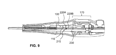
Turning now to FIG. 9, a replaceable tip with matching circuit 215 and joint
205 is
shown. A replaceable tip with matching circuit 215 may be connected to a
handle
body through a joint 205. Similar to the circuit seen in FIG. 7, the matching
circuit
215 may contain a series capacitance 100 and parallel capacitance 110.
Electronically
controlled capacitors 220A, 220B may be used to adjust the effective series
and
parallel capacitance for impedance matching.
The electronically controlled capacitor values 220A, 220B may be set at
manufacturing. After assembly of the replaceable tip electronics, the
replaceable tip
may be connected to a power source 20 (FIG. 2). Electronically controlled
capacitors
may be adjusted until an acceptable SWR or near minimum SWR has been obtained.
The electronically controlled capacitors may then have their settings stored
with the
matching circuit 215, as described in more detail.
Storing settings or controlling components of the matching circuit may be
accomplished through multiple methods. According to one aspect of the
invention, a
processor 230 may store the settings in non-volatile memory. Alternatively,
fuses
may be used, such that by "blowing" a fuse, or rendering it inactive, a
different setting
is stored. According to another aspect, circuit traces may be joined, such
that each
joining of a trace causes a different setting to be stored.
In another embodiment, a processor 230 may monitor the SWR and adjust the
electronically controlled capacitors. It may be desirable to have an active
method of
minimizing the SWR. By actively monitoring SWR, a system may be operable over
more than a narrow frequency band. Thus, if different frequencies are
desirable in
different instances, an operator may choose the most effective frequency and
the
matching circuit 215 may automatically match the new impedance of the source,
line
and/or load.
According to one aspect of the present invention, the sensor 232 may monitor
SWR and the information gathered by the sensor 232 may be used to adjust
controllable capacitors, controllable inductors, controllable resistors,
and/or other
controllable components which might make up the matching circuit 215 according
to
principles discussed herein. In some embodiments, a matching circuit may be
made
CA 02868742 2014-09-26
WO 2013/106036
PCT/US2012/032661
14
more useful over a larger range of devices by including variable inductance,
capacitance and/or resistance in the matching circuit. The matching circuit
may thus
be able to accommodate more surgical elements and/or more frequencies.
The sensor 232 may monitor SWR or another indicator which provides
information regarding the efficiency of power transfer from a power source to
the
surgical instrument. Thus, when the indicator, such as SWR, suggests that
power is
being lost in transmission to the surgical instrument, the circuit may be
adjusted so
that power transfer is improved or maximized. In the case of SWR, the matching
circuit may attempt to make adjustments to achieve SWR of 1:1 that may provide
a
desired response of better power transfer to the surgical element. The circuit
may use
variable inductors, capacitors, transformers, transmission lines, resistors,
and/or
combinations of the foregoing to accomplish this goal.
The overall goal of the present invention is to provide for tuning of a
thermal
surgical instrument by transforming the impedance of a load, for example the
load of
a thermal element such as a ferromagnetic tip, to match that of a transmission
line
connecting a power source to the thermal element. For example, the
transmission line
which carries the RF current from a power source to a surgical handpiece may
be 50
ohms. The thermal element, such as a ferromagnetic tip may have a load of, for
example, 2+i18 ohms. To transform the inductive load of the thermal element to
a
50+i0.0 ohm load to match the characteristic impedance of the transmission
line,
components such as capacitors, coaxial cables, varactors, and sometimes more
inductors may be used.
A Smith chart may be used to determine which components will make up the
matching circuit. The Smith chart is plotted on the complex reflection
coefficient
plane in two dimensions and may be scaled in normalized impedance. The Smith
chart has circumferential scaling in wavelengths and degrees. The wavelengths
scale
is used in distributed component problems and represents the distance measured
along
the transmission line connected between the generator or source and the load
to the
point under consideration. The degrees scale represents the angle of the
voltage
reflection coefficient at that point.
For example a Smith chart having a normalized impedance of 50 ohms may be
used to design a matching circuit for matching the impedance of a load with
the
CA 02868742 2014-09-26
WO 2013/106036
PCT/US2012/032661
impedance of a transmission line having a characteristic impedance of 50 ohms.
FIGs.
10A-10D show several examples of how one might transform the impedance of the
load of a surgical tip of the present invention. It will be appreciated that
there are a
variety methods, other than using a Smith chart, which may be used to design a
5 matching circuit of the present invention. Furthermore, those skilled in
the art will
appreciate that examples shown in FIGs. 10A-10D are not exhaustive of how the
load
may be matched to the characteristic impedance of a transmission line.
Turning now to FIG. 10A, there is shown a Smith chart having a normalized
impedance of 50 ohms for designing a matching circuit for a transmission line
having
10 a characteristic impedance of 50 ohms. It will be appreciated that
transmission lines
having different characteristic impedance values may be used with a thermal
surgical
instrument of the present invention, however, for ease of illustration the
Smith chart
discussed herein all have normalized impedance of 50 ohms. FIG. 10A
illustrates
how capacitors may be used to transform the load of a surgical tip 250 to
match the
15 source impedance of a transmission line 260. The load of the surgical
tip 250 is 2+i18
ohms. Capacitors connected in series and parallel may be used to transform the
load
of the surgical to about 50+i0.0 ohms. The Smith chart may be used to
determine the
proper capacitance to match the load 250 to the characteristic impedance of
the
transmission line. For example, the load 250 may be matched using a series
capacitance 280 of about 52 pF and a parallel capacitance 270 of about 179 pF.
A
schematic 290 of the matching circuit is also shown in FIG. 10A.
FIG. 10B illustrates how a length of coaxial cable and capacitors may be used
match the load of a surgical tip 250 with a source impedance 260. A series
capacitance 280 of about 49 pF and a coaxial cable 270 may be used to
transform the
load 2+i18 of the surgical tip 250 to about 50+i0.0 so that it substantially
matches the
source impedance 260. A schematic 320 of such a matching circuit is also shown
in
FIG. 10B.
FIG. 10C illustrates how capacitors and inductors may be used match the load
of a
surgical tip 250 with a source impedance 260. A series capacitance 350 of
about 79
pF, a parallel capacitance 340 of about 235 pF, and an inductance 330 of about
35 nH
may be used to transform the load 2+i5 of the surgical tip 250 to about
50+i0.0 so that
it substantially matches the source impedance 260. The matching circuit of
FIG. 10C
CA 02868742 2014-09-26
WO 2013/106036
PCT/US2012/032661
16
may be particularly useful with surgical tips which have very low impedance. A
schematic 360 of such a matching circuit is also shown in FIG. 10C.
FIG. 10D illustrates how a capacitor and transformer may be used to match the
load of a surgical tip 250 with a source impedance 260. A series capacitance
380 of
about 31 pF and a transformer having a primary to secondary turn ratio of
1:5.00
(represented by reference numeral 370) may be used to transform the load 2+i5
of the
surgical tip 250 to about 50+i0.0 so that it substantially matches the source
impedance
260. A schematic 390 of such a matching circuit is also shown in FIG. 10D.
FIGs. 11A to 42 show various embodiments of surgical elements and handpieces
that may benefit from an impedance matching circuit using the techniques and
construction described above.
Turning now to FIGs. 11A to 13B, a surgical handpiece is shown with a power
source, control and handpiece. The surgical element may be a ferromagnetic
covered
conductor. Figure 13B shows an autotransformer, which may be another way of
matching the load of the thermal element of a surgical tool to a power source.
Turning now to FIGs. 14 to 33, various tip geometries are shown. Each tip
configuration may require different base impedance matching circuit component
values as well as individual adjustments due to manufacturing tolerances. Tip
configurations such as geometry, thicknesses of layers, composition, and
length, may
all require different matching circuit component values.
Turning now to FIGs. 34 to 42, various surgical tools are shown. The impedance
matching circuits may be used with different surgical tools and/or modalities
such as
catheters (FIG. 34), thermal surgical tools (FIG. 35), mono-polar
electrosurgical tools
(FIG. 36), bipolar electrosurgical tools (FIG. 38), ultra-sonic surgical tools
(FIG.
41A), and multi-mode surgical tools that may combine multiple surgical
modalities
into one instrument, such as a thermal and bipolar surgical modality.
Turning now to FIG. 43, a thermal spectrum as related to tissue effects is
shown.
With efficient power transfer, such as may be achieved with a correctly
adjusted
matching circuit, a smaller power source may be used to achieve desired tissue
effects
than would be required with an inefficient power transfer.
It will be understood that the invention includes a number of aspects and that
those
aspect may be utilized in a variety of ways. For example, in accordance with
the
CA 02868742 2014-09-26
WO 2013/106036
PCT/US2012/032661
17
present invention, a thermal surgical instrument may include: a thermal
element
configured to generate thermal energy in response to an electrical signal; and
a
matching circuit electrically connected to the thermal element, the matching
circuit,
in combination with the thermal element, having an input impedance. The
thermal
surgical instrument may also include: the thermal surgical instrument being
connectable to a power source and the input impedance matching the output
impedance of the power source; the thermal surgical instrument being
connectable to
a power source via a transmission line, and the input impedance matching the
impedance of the transmission line; a sensor to monitor an indicator of
efficiency of
power transfer to the thermal surgical instrument; the input impedance being
adjustable; the input impedance being electronically adjustable; the matching
circuit
having at least one component selected from the group of a capacitor,
inductor,
variable capacitor, variable inductor, transformer, coaxial cable, and
varactor; the
matching circuit having a conductive layer disposed on a substrate and at
least a
portion of the conductive layer being removable; the thermal element having a
ferromagnetic material disposed on an electrical conductor; a data storage
unit to store
a setting of the thermal surgical element; and/or the data storage unit being
an
EEPROM, or combinations thereof.
A method of matching an input impedance of a load of a thermal surgical
instrument with an output impedance of a power source in accordance with the
present invention may include: selecting a thermal surgical tool having a
thermal
element and a circuit board; and disposing a component on the circuit board to
form a
matching circuit, wherein the thermal element and the matching circuit have a
load
having an adjustable input impedance. The method may also include: measuring
an
indicator of the load and adjusting the component so that the adjustable input
impedance is substantially equal to an output impedance of a transmission line
connecting a power source to the thermal surgical instrument; disposing a
second
component on the board to form the matching circuit; using a component having
a
conductive layer, and removing at least a portion of the conductive layer to
adjust the
input impedance; measuring the indicator as the standing wave ratio on the
transmission line caused by impedance mismatch interaction between the load
and
source, and adjusting the component such that the standard wave ratio is
substantially
CA 02868742 2014-09-26
WO 2013/106036
PCT/US2012/032661
18
1:1; adjusting the components electronically; and/or using a component in the
form of
a varactor, and controlling a voltage applied to the varactor to adjust the
input
impedance, or combinations thereof.
A method of manufacturing a thermal surgical instrument may include:
selecting a surgical instrument comprising a thermal element, disposing a
matching
circuit in electrical communication with the thermal element such that the
matching
circuit, in combination with the thermal element, has an input impedance,
adjusting
the input impedance so that it matches an output impedance of a power source.
The
method may also include: disposing a data storage unit on the thermal surgical
instrument, and the data storage unit storing settings of the thermal surgical
instrument; disposing a sensor on the thermal surgical element for monitoring
an
indicator of the thermal element; and/or using a matching circuit which has a
conductive layer and adjusting the input impedance by removing at least a
portion of
the conductive layer, or combinations thereof.
CA 02868742 2014-09-26
WO 2013/106036
PCT/US2012/032661
19
There is thus disclosed an improved impedance matching circuit. It will be
appreciated that numerous changes may be made to the present invention without
departing from the scope of the claims.