Note: Descriptions are shown in the official language in which they were submitted.
CA 02870426 2014-10-14
DESCRIPTION
Title of Invention
METHOD FOR PRODUCING MOLD FOR TRANSFERRING FINE PATTERN,
METHOD FOR PRODUCING SUBSTRATE HAVING UNEVEN STRUCTURE USING
SAME, AND METHOD FOR PRODUCING ORGANIC EL ELEMENT HAVING SAID
SUBSTRATE HAVING UNEVEN STRUCTURE
TECHNICAL FIELD
[0001] The present invention relates to a method for producing a mold for
transferring a
minute (fine) pattern usable for nano-imprinting, etc., a method for producing
a substrate
having a concave-convex structure (concavity and convexity structure, uneven
or irregular
structure) using the mold, a method for producing an organic electro-
luminescent (EL)
element provided with the substrate having the concave-convex structure, a
mold for
transferring a fine pattern, a substrate having a concave-convex structure,
and an organic
EL element which are obtained by using one of the producing methods.
BACKGROUND ART
[0002] The lithography method is known as a method for forming a fine pattern
such as a
semiconductor integrated circuit. The resolution of a pattern formed by the
lithography
method depends on the wavelength of a light source, the numerical aperture of
an optical
system, etc., and a shorter wavelength light source is desired so as to
respond to the
demand for miniaturized devices in the recent years. Any short wavelength
light source
is, however, expensive and is not easily developed, and any optical material
allowing such
short wavelength light passing therethrough needs to be developed, as well.
Further, a
large sized optical element is required for producing a pattern with a large
area by means
of the conventional lithography method, which is difficult both technically
and
economically. Therefore, a new method for forming a desired pattern having a
large area
has been considered.
[0003] The nano-imprinting method is known as a method for forming a fine
pattern
without using any conventional lithography apparatus. The nano-imprinting
method is a
1
CA 02870426 2014-10-14
technique capable of transferring a pattern in nano-meter order by sandwiching
a resin
between a mold and a substrate, and basically is composed of the following
four steps of:
(i) coating with a resin layer (application of a resin layer), (ii) pressing
with the mold, (iii)
transferring of the pattern and (iv) releasing of the mold (mold-releasing).
Thus, the
nano-imprint method is excellent in that the nano-sized processing can be
realized with
such a simple process. Further, in the nano-imprint method, devises or
apparatuses used
therefor are simple, the processing can be performed for a large area as well
as a high
throughput can be expected. Accordingly, the nano-imprint method is expected
to be
practiced not only in the field of semiconductor device but also in many
fields such as
storage media, optical members, biochips, etc.
[0004] In the nano-imprint method as described above, however, a mold for
transferring a
pattern having a line width of several tens of nanometers (nm) needs to be
formed basically
by exposing a resist on a silicon substrate and developing the resist to form
a resist pattern
(a pattern of a resist), with a lithography apparatus. Further, an electric
current seed layer
(current seed layer) made of a metal is formed on the resist pattern for
performing
electroforming (electroplating) of the mold by using the obtained resist
pattern. However,
in a case that the pattern fineness is not more than 100 nm, the coating
performance
(coatability or coverage) of the current seed layer formed on the pattern by
sputtering is
lowered, which in turn causes such a state that the film thickness (thickness)
of the
obtained current seed layer is different or non-uniform among an upper
portion, a side wall
portion and a bottom portion of the resist pattern (the bottom portion being a
substrate-exposure portion in which the substrate is exposed in a recessed
portion in the
pattern, namely in a trench). In particular, the formation of the current seed
layer is
progressed preferentially in the upper portion of the resist pattern, thereby
causing such a
problem that the opening of the trench is constricted or narrowed.
Consequently, in a
case that holes or trenches and ridges are formed on the substrate by using
the resist layer,
there is such a problem that the metal of the current seed layer is hardly
deposited in the
bottom portions of the holes or trenches, and that any overhang is generated
at the upper
portions of the ridges of the resist layer. When any stacked body with such a
current seed
layer is subjected to the electroforming, an electroplating film is joined at
a portion above
the hole or trench due to the overhang, leaving a void inside the trench. As a
result, a
mold obtained by the electrofonning has low mechanical strength, which in turn
causes
such a problem including defect exemplified by any deformation of the mold,
deficit
2
CA 02870426 2014-10-14
(chipped) pattern, etc.
[0005] In order to solve the above problem, Patent Literature 1 discloses a
method for
producing a mold for nano-imprint including the steps of:
forming a resist layer having a concave-convex pattern, which is composed of
concave portions and convex portions (concavities and convexities), on a
substrate having
a conductive surface and causing the conductive surface to be exposed at the
concave
portions of the concave-convex pattern of the resist layer;
performing electroforming on the conductive surface exposed at the concave
portions of the concave-convex pattern of the resist layer to form a
electroforming film
having a thickness greater than a thickness of the resist layer; and
removing the substrate having the conductive surface and the resist layer.
Since this method is capable of growing the electroforming film in
unidirectional
manner upwardly from the conductive surface at the bottom portion of the
resist pattern
without using a current seed layer, it is considered that any void is not
present inside the
mold for nano-imprint. Even with this method, however, the mold used in the
nano-imprint method should be made with the lithography method, same as
before.
[CITATION LIST]
[PATENT LITERATURE]
[0006]
PATENT LITERATURE 1: Japanese Patent Application Laid-open No.
2010-017865
PATENT LITERATURE 2: PCT International Publication No.
W02011/007878A1
PATENT LITERATURE 3: Japanese Patent Application Laid-open No.
2010-056256
SUMMARY OF INVENTION
Problem to be Solved by the Invention:
100071 The inventors of the present invention disclose the following method in
PATENT
LITERATURE 2. Namely, a block copolymer solution containing a block copolymer
satisfying a predetermined condition and a solvent is applied on a base member
(the base
3
CA 02870426 2014-10-14
member is coated with the block copolymer solution), and drying is performed
for the
applied block copolymer solution to form a micro phase separation structure of
the block
copolymer, thereby obtaining a master block (mold) in which a fine (minute)
and irregular
concave-convex pattern is formed. According to this method, it is possible to
obtain the
master block usable for the nano-imprint and the like by using a self-
organizing
phenomenon of the block copolymer, without using the lithography method. A
mixture of
a silicone-based polymer and a curing agent is dropped onto the obtained
master block and
then cured to obtain a transferred pattern. Then, a glass substrate coated
with a curable
resin is pressed to (against) the transferred pattern and the curable resin is
cured by
irradiation with an ultraviolet light. In this way, a diffraction grating in
which the
transferred pattern is duplicated is manufactured. It has been confirmed that
an organic
EL diode (organic light-emitting diode) obtained by stacking a transparent
electrode, an
organic layer, and a metal electrode on the diffraction grating has
sufficiently high light
emission efficiency, sufficiently high level of external extraction
efficiency, as well as
sufficiently low wavelength-dependence of light emission, sufficiently low
directivity of
light emission, and sufficiently high power efficiency.
[0008] In this method, however, a step is required for removing one of
polymers
composing the block copolymer with the etching process, so as to obtain the
concave-convex pattern after the formation of the micro phase separation
structure of the
block copolymer. Due to this removing step, one of the polymers is removed as
portions
at each of which the base member is exposed and the other of the polymers is
remained to
form the convex portions. However, the remaining convex portions have small
area of
contact with the surface of the base member, and thus easily drop off or
detach from the
surface of the base member. Further, there is a case that any foreign matter
adheres to the
base member and/or the surfaces of the convex portions accompanying with the
etching
process, which in turn presents a possibility that the master block or a
diffraction grating
produced from the master block via a transfer process might be contaminated.
If these
cases happened in a mass production process of diffraction gratings, there is
a fear that the
throughput might be lowered in the mass production process of diffraction
gratings or of
organic EL elements produced by using the diffraction gratings. Therefore,
there is a
demand to further advance the method for producing the diffraction grating
achievable in
the preceding patent application by the inventors of the present invention
(Patent Literature
2), for the purpose of providing a production method further suitable for mass
production
4
CA 02870426 2014-10-14
of products such as organic EL elements, etc.
[0009] Patent Literature 3 disclose forming a columnar-shaped micro domain
structure,
lamella-type micro domain structure, etc., by phase-separating a high polymer
layer
including a block copolymer of which molecular weight is relatively low. This
method,
however, removes one of the polymers by the etching, etc., for the patterning
purpose.
[0010] In view of the above situation, an object of the present invention is
to provide a
method for producing a mold for transferring a fine pattern suitable for mass-
producing a
substrate having a concave-convex structure such as a diffraction grating
usable for a
general-purpose item such as an organic EL element, a method for producing a
substrate
having a concave-convex structure by using the obtained mold, and a method for
producing an organic EL element using the substrate having such concave-convex
structure. Another object of the present invention is to produce a mold for
transferring a
fine pattern, a substrate having a concave-convex structure, and an organic EL
element
with a high throughput by using one of these producing methods.
Solution to the Problem:
100111 According to the present invention, there is provided a method for
producing a
mold for transferring a fine pattern, the method including:
a step of coating a surface of a base member with a solution containing a
block
copolymer and polyalkylene oxide, the block copolymer being composed of at
least first
and second polymer segments;
a solvent phase-separation step of phase-separating the block copolymer
contained
in the solution, with which the surface of the base member is coated, under a
presence of
vapor of an organic solvent so as to obtain a block copolymer film of the
block copolymer,
the block copolymer film having a concave-convex structure on a surface
thereof and a
horizontal cylinder structure in an interior thereof;
a step of forming a seed layer on the concave-convex structure of the block
copolymer film;
a step of stacking a metal layer on the seed layer by electroforming; and
a step of releasing the base member, on which the concave-convex structure is
formed, from the metal layer.
[0012] In the method for producing the mold of the present invention, a volume
ratio
between the first and second polymer segments in the block copolymer is
preferably in a
CA 02870426 2014-10-14
range of 4:6 to 6:4, in view of generating the horizontal cylinder structure.
Further, a
content amount of the polyalkylene oxide is preferably in a range of 5 parts
by mass to 70
parts by mass relative to 100 parts by mass of the block copolymer, in view of
obtaining
sufficient height (groove depth) of the concave-convex structure. Furthermore,
number
average molecular weight of the block copolymer is preferably not less than
500,000.
Since a wave-like (wave-like shaped) concave-convex structure can be obtained
by the
solvent phase-separation step in the producing method of the present
invention, any
etching process is not necessary after the solvent phase-separation process
(step).
100131 In the method for producing the mold of the present invention, the
first polymer
segment composing the block copolymer may be polystyrene; the second polymer
segment
composing the block copolymer may be polymethyl methacrylate. Further, the
organic
solvent may be one selected from the group consisting of chloroform, acetone,
dichloromethane, and a mixed solvent of carbon bisulfide and acetone. Further,
a time
for phase-separating the block copolymer under the presence of the vapor of
the organic
solvent may be in a range of 6 hours to 168 hours.
100141 In the method for producing the mold of the present invention, even in
a case that
the first or second polymer segment is formed to have a one-tiered (one-stage)
structure or
a two-tiered (two-stage) structure in the horizontal cylinder structure, the
concave-convex
structure appears on the surface. As the mold for the substrate having the
concave-convex structure such as a diffraction grating, it is desirable that
an average value
of depth distribution of concavities and convexities of the concave-convex
structure is in a
range of 20 nm to 200 nm, preferably in a range of 30 nm to 150 nm; and that
standard
deviation of depth of the concavities and convexities is in a range of 10 nm
to 100 nm,
more preferably in a range of 15 nm to 75 nm.
100151 In the method for producing the mold of the present invention, it is
preferable that
a primer layer is formed on the surface of the base member before coating the
surface of
the base member with the solution containing the block copolymer, which is
composed of
at least the first and second polymer segments, and the polyalkylene oxide.
Further,
molecular weight distribution (Mw/Mn) of the block copolymer is preferably not
more
than 1.5, and difference in solubility parameter between the first and second
polymer
segments is in a range of 0.1 (cal/cm3)1/2 to 10 (cal/cm3)1/2.
100161 According to a second aspect of the present invention, there is
provided a method
for producing a diffraction grating, the method including:
6
CA 02870426 2014-10-14
pressing a mold obtained by the above method for producing the mold onto
(against) a substrate coated with a concavity-convexity forming material and
curing the
concavity-convexity forming material, and removing the mold from the substrate
so as to
form a diffraction grating having a concave-convex structure on the substrate.
[0017] According to a third aspect of the present invention, there is provided
a method
for producing a diffraction grating, the method including:
pressing a mold obtained by the above method for producing the mold onto a
substrate coated with a concavity-convexity forming material, curing the
concavity-convexity forming material, and removing the mold from the substrate
so as to
form a structure having a concave-convex structure on the substrate; and
pressing the structure onto another substrate coated with a sol-gel material,
curing
the sol-gel material, and removing the structure from the another substrate so
as to form a
diffraction grating having a concave-convex structure formed of the sol-gel
material.
[0018] According to a fourth aspect of the present invention, there is
provided a method
for producing an organic EL element, the method including: stacking a
transparent
electrode, an organic layer and a metal electrode successively on a concave-
convex
structure of a diffraction grating, produced by the above method of producing
the
diffraction grating, so as to form the organic EL element.
[0019] According to a fifth aspect of the present invention, there is provided
a mold for
transferring a fine pattern produced by the above method for producing the
mold.
[0020] According to a sixth aspect of the present invention, there is provided
a diffraction
grating which is produced by the above method for producing the diffraction
grating and
which has a concave-convex structure on a surface thereof. The diffraction
grating has an
average pitch of concavities and convexities of the concave-convex structure
which is
preferably in a range of 100 nm to 1,500 nm, more preferably in a range of 200
nm to
1,200 nm. Further, a cross-sectional shape of the concave-convex structure is
preferably
wave-like; and that in a case of obtaining a Fourier-transformed image by
performing a
two-dimensional fast Fourier-transform processing on a concavity and convexity
analysis
image obtained by analyzing a planer shape of the concave-convex structure
with an
atomic force microscope, the Fourier-transformed image preferably shows an
annular
pattern substantially centered at an origin at which an absolute value of
wavenumber is 0
-1
gm , and the annular pattern is present within a region where the absolute
value of
wavenumber is within a range of not more than 10 gm-1. Furthermore, kurtosis
of a
7
CA 02870426 2014-10-14
cross-sectional shape of the concave-convex structure of the diffraction
grating is
preferably not less than -1.2, more preferably in a range of -1.2 to 1.2.
[0021] According to a seventh aspect of the present invention, there is
provided an
organic EL element produced by the above method for producing the organic EL
element.
[0022] According to an eighth aspect of the present invention, there is
provided a method
for producing a substrate having a concave-convex structure, the method
including:
pressing a mold obtained by the above method for producing the mold onto a
substrate
coated with a concavity-convexity forming material, curing the concavity-
convexity
forming material, and removing the mold from the substrate so as to form the
substrate
having a concave-convex structure.
[0023] According to a ninth aspect of the present invention, there is provided
a method
for producing a substrate having a concave-convex structure, the method
including:
pressing a mold obtained by the above method for producing the mold onto a
substrate coated with a concavity-convexity forming material, curing the
concavity-convexity forming material, and removing the mold from the substrate
so as to
form a structure having a concave-convex structure on the substrate; and
pressing the structure onto another substrate coated with a sol-gel material,
curing
the sol-gel material, and removing the structure from the another substrate so
as to form the
a substrate having a concave-convex structure formed of the sol-gel material.
[0024] According to a tenth aspect of the present invention, there is provided
a substrate
having a concave-convex structure on a surface thereof and produced by the
above method
of producing the substrate. The substrate having the concave-convex structure
has an
average pitch of concavities and convexities of the concave-convex structure
which is
preferably in a range of 100 nm to 1,500 nm, more preferably in a range of 200
nm to
1,200 nm.
Effects of Invention:
[0025] According to the method for producing the mold of the present
invention, a block
copolymer film of which surface has a smooth and wave-like concave-convex
structure
and of which cross-sectional structure has a horizontal cylinder structure can
be obtained
by phase-separating the solution, which contains the block copolymer, with the
organic
solvent so as to cause the self-organization of the block copolymer. Thus, the
etching
step which has been required for forming the concave-convex structure becomes
8
CA 02870426 2014-10-14
unnecessary, thereby realizing a simplified production process and lowering
the possibility
that any dirt (stain, soil, dust) and/or any foreign matter might adhere to
the mold through
the production process, as well. The surface property of a metal layer of the
obtained
mold is such that smooth concavities and convexities are distributed
substantially
uniformly, and that a resin is suppressed from remaining on a side of the mold
when the
block copolymer and the base member are released (peeled off) from the mold,
thereby
enhancing the releasing property (peeling property) of the mold. With this,
any pattern
defect is prevented from generating. Further, even in a case that the
molecular weight of
the block copolymer is as high as 500,000 or more, it is possible to form a
mold having a
desired concave-convex pattern in an ensured manner. Therefore, by using a
mold
obtained by the present invention, a substrate having the concave-convex
structure, such as
a diffraction grating diffracting a light of the visible region without any
wavelength
dependency and with low directivity, can be produced with a relatively low
cost and with a
high throughput.
BRIEF DESCRIPTION OF DRAWINGS
100261
Fig. 1(A) to 1(F) is a view conceptually showing the steps in a mold-producing
method of the present invention.
Fig. 2(A) to 2(E) is a view conceptually showing the steps for producing a
diffraction grating using a mold obtained by the mold-producing method of the
present
invention.
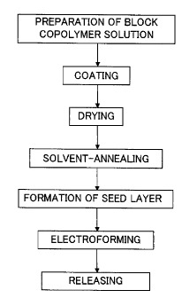
Fig. 3 is a flowchart showing the steps in the mold-producing method of the
present invention.
Fig. 4 is a conceptual view of a roll processing apparatus for producing a
film-shaped substrate as a mold to be used in a diffraction-grating producing
method.
Fig. 5 is a flowchart showing steps for producing a concave-convex substrate,
which has concavities and convexities made of a sol-gel material, by using the
film-shaped
substrate as the mold.
Fig. 6 is a conceptual view for explaining a roll processing for performing
transfer
on the sol-gel material by using the film-shaped substrate as the mold.
Fig. 7 is a conceptual view showing a stacked structure of an organic EL
element
by using a diffraction grating obtained by the diffraction-grating producing
method of the
9
CA 02870426 2014-10-14
present invention.
Fig. 8A is a photograph of the cross section of a thin film, obtained by
Example 1,
after solvent annealing observed by a transmission electron microscope,
showing a
two-tiered (two-stage) horizontal cylinder structure.
Fig. 8B is an enlarged photograph of the photograph of Fig. 8A.
Fig. 8C is a photograph of the cross section of the thin film, obtained by
Example
1 after solvent annealing, observed by the transmission electron microscope,
showing a
one-tiered (one-stage) horizontal cylinder structure.
Fig. 8D is an enlarged photograph of the photograph of Fig. 8C.
Fig. 9A is a photograph showing a concavity and convexity analysis image,
taken
by an atomic force microscope, of a surface of a concave-convex structure of
the thin film
obtained in Example 1.
Fig. 9B is a photograph showing a concavity and convexity analysis image,
taken
by the atomic force microscope, of the cross section at a portion in the
vicinity of the
surface of the concave-convex structure of the thin film shown in Fig. 9A.
Fig. 9C is a photograph showing a Fourier-transformed image obtained based on
the concavity and convexity analysis images shown in Figs. 9A and 9B.
Fig. 10A is a photograph showing a concavity and convexity analysis image,
taken
by an atomic force microscope, of a surface of a concave-convex structure of a
thin film
obtained in Comparative Example 1.
Fig. 10B is a photograph showing a concavity and convexity analysis image,
taken
by the atomic force microscope, of the cross section at a portion in the
vicinity of the
surface of the concave-convex structure of the thin film shown in Fig. 10A.
Fig. 10C is a photograph showing a Fourier-transformed image obtained based on
the concavity and convexity analysis images shown in Figs. 10A and 10B.
Fig. 11 is a graph showing the change in electric current efficiency with
respect to
the luminance (brightness) of an organic EL element produced in Example 7.
Fig. 12 is a graph showing the change in electric power efficiency with
respect to
the luminance of the organic EL element produced in Example 7.
DESCRIPTION OF EMBODIMENTS
100271 In the following, a preferred embodiment of the present invention will
be
CA 02870426 2014-10-14
described in detail with reference to the drawings.
[0028] At first, an explanation will be given about a mold-producing method
for
producing a mold suitable for producing a substrate having a concave-convex
structure
such as a diffraction grating usable for an organic EL element. As shown in a
flowchart
of Fig. 3, the mold-producing method mainly includes a step for preparing a
solution of
block copolymer (block copolymer solution), a step of coating a base member
with the
block copolymer solution (applying the block copolymer solution), a drying
step, a solvent
annealing step, a step of forming a seed layer, an electroforming step and a
releasing step
(peeling step). In the following, an explanation will be given about the
respective steps of
the mold-producing method and steps following the mold-producing method, also
referring
to the conceptual views shown in Figs. 1 and 2. Note that although the
following
explanation is given about a diffraction grating substrate as an example of a
substrate
having concave-convex structure, a substrate having the concave-convex
structure
according to the present invention is not limited to the optical substrate
such as the
diffraction grating substrate and is applicable also to a variety of
substrates having various
applications, as will be described later on.
100291
[Preparation step of block copolymer solution]
The block copolymer used for present invention includes at least a first
polymer
segment made of a first homopolymer and a second polymer segment made of a
second
homopolymer different from the fist homopolymer. The second homopolymer
desirably
has a solubility parameter which is higher than a solubility parameter of the
first
homopolymer by 0.1 (cal/cm3)1/2 to 10 (cal/cm3)1/2. In a case that the
difference in the
solubility parameter between the first and second homopolymers is less than
0.1
(cal/cm3)1/2, it is difficult to form a regular micro phase separation
structure of the block
copolymer. In a case that the difference exceeds 10 (cal/cm3)1/2, it is
difficult to prepare a
uniform solution of the block copolymer.
100301 Examples of monomers serving as raw materials of homopolymers usable as
the
first homopolymer and second homopolymer include styrene, methylstyrene,
propylstyrene,
butylstyrene, hexylstyrene, octylstyrene, methoxystyrene, ethylene, propylene,
butene,
hexene, acrylonitrile, acrylamide, methyl methacrylate, ethyl methacrylate,
propyl
methacrylate, butyl methacrylate, hexyl methacrylate, octyl methacrylate,
methyl acrylate,
ethyl acrylate, propyl acrylate, butyl acrylate, hexyl acrylate, octyl
acrylate, methacrylic
11
CA 02870426 2014-10-14
acid, acrylic acid, hydroxyethyl methacrylate, hydroxyethyl acrylate, ethylene
oxide,
propylene oxide, dimethylsiloxane, lactic acid, vinylpyridine, hydroxystyrene,
styrenesulfonate, isoprene, butadiene, c-caprolactone, isopropylacrylamide,
vinyl chloride,
ethylene terephthalate, tetrafluoroethylene, and vinyl alcohol. Among these
monomers,
styrene, methyl methacrylate, ethylene oxide, butadiene, isoprene,
vinylpyridine, and lactic
acid are preferably used from the viewpoints that the formation of phase
separation easily
occurs, and that concavities and convexities of the concave-convex structure
are easily
formed by an etching.
100311 Further, examples of a combination of the first homopolymer and the
second
homopolymer may include combinations of two selected from the group consisting
of a
styrene-based polymer (more preferably, polystyrene), polyalkyl methacrylate
(more
preferably, polymethyl methacrylate), polyethylene oxide, polybutadiene,
polyisoprene,
polyvinylpyridine, and polylactic acid. Among these combinations, a
combination of the
styrene-based polymer and polyalkyl methacrylate, a combination of the styrene-
based
polymer and polyethylene oxide, a combination of the styrene-based polymer and
polyisoprene, a combination of the styrene-based polymer and polybutadiene are
more
preferable, and the combination of the styrene-based polymer and polymethyl
methacrylate,
the combination of the styrene-based polymer and polyisoprene, the combination
of the
styrene-based polymer and polybutadiene are particularly preferable. A
combination of
polystyrene (PS) and polymethyl methacrylate (PMMA) is further preferable from
the
viewpoint of obtaining a preferable number average molecular weight (Mn) of
the block
copolymer.
[0032] The number average molecular weight (Mn) of the block copolymer is
preferably
not less than 500,000, and more preferably not less than 1,000,000, and
particularly
preferably in a range of 1,000,000 to 5,000,000. The domain size of the block
copolymer
increases as the molecular weight thereof increases. In a case that the number
average
molecular weight is less than 500,000, the average pitch of the concavities
and convexities
formed by the micro phase separation structure of the block copolymer is so
small that the
average pitch of the concavities and convexities of the obtained diffraction
grating
becomes insufficient. Especially, in a case of the diffraction grating used
for the organic
EL, the diffraction grating needs to diffract illumination light over a range
of wavelength
of the visible region, and thus the average pitch is desirably in a range of
100 nm to 1,500
nm, more desirably in a range of 200 nm to 1,200 nm. In view of this point,
the number
12
CA 02870426 2014-10-14
average molecular weight (Mn) of the block copolymer is preferably not less
than 500,000.
[0033] The molecular weight distribution (Mw/Mn) of the block copolymer is
preferably
not more than 1.5, and is more preferably in a range of 1.0 to 1.35. In a case
that the
molecular weight distribution exceeds 1.5, it is difficult to form the regular
micro phase
separation structure of the block copolymer.
[0034] Note that the number average molecular weight (Mn) and the weight
average
molecular weight (Mw) of the block copolymer are values measured by the gel
permeation
chromatography (GPC) and converted to the molecular weights of standard
polystyrene.
[0035] In the block copolymer, the volume ratio between the first polymer
segment and
the second polymer segment (the first polymer segment: the second polymer
segment) is
desirably in a range of 4:6 to 6:4 in order to generate a horizontal cylinder
structure by
self-organization or assembly (to be described later on), and is more
preferably about 5:5.
In a case that the volume ratio is out of the above-described range, it is
difficult to form a
concave-convex pattern (concavity and convexity pattern) owing to the
horizontal cylinder
structure (to be described later on) and there is a tendency that a globular
or spherical
structure or vertical cylinder structure appears.
[0036] The block copolymer solution used in the present invention is prepared
by
dissolving the block copolymer in a solvent. Examples of the solvent include
aliphatic
hydrocarbons such as hexane, heptane, octane, decane, and cyclohexane;
aromatic
hydrocarbons such as benzene, toluene, xylene, and mesitylene; ethers such as
diethyl ether,
tetrahydrofuran, and dioxane; ketones such as acetone, methyl ethyl ketone,
isophorone,
and cyclohexanone; ether alcohols such as butoxyethyl ether, hexyloxyethyl
alcohol,
methoxy-2-propanol, and benzyloxyethanol; glycol ethers such as ethylene
glycol dimethyl
ether, diethylene glycol dimethyl ether, triglyme, propylene glycol monomethyl
ether, and
propylene glycol monomethyl ether acetate; esters such as ethyl acetate, ethyl
lactate, and
y-butyrolactone; phenols such as phenol and chlorophenol; amides such as
N,N-dimethylformamide, N,N-dimethylacetamide, and N-methylpyrrolidone;
halogen-containing solvents such as chloroform, methylene chloride,
tetrachloroethane,
monochlorobenzene, and dichlorobenzene; hetero-element containing compounds
such as
carbon disulfide; and mixture solvents thereof. The percentage content of the
block
copolymer in the block copolymer solution is preferably in a range of 0.1% by
mass to
15% by mass, and more preferably in a range of 0.3% by mass to 5% by mass,
relative to
100% by mass of the block copolymer solution.
13
CA 02870426 2014-10-14
[0037] In addition, the block copolymer solution further contains polyalkylene
oxide as a
different homopolymer (a homopolymer other than the first homopolymer and the
second
homopolymer in the block copolymer contained in the solution: for example, in
a case that
the combination of the first homopolymer and the second homopolymer in the
block
copolymer is the combination of polystyrene and polymethyl methacrylate, the
different
homopolymer may be any kind of homopolymer other than polystyrene and
polymethyl
methacrylate).
[0038] By allowing the block copolymer solution to contain polyalkylene oxide,
the
depth of the concavities and convexities formed by the micro phase separation
structure of
the block copolymer can be increased. As the polyalkylene oxide, polyethylene
oxide or
polypropylene oxide is more preferable, and polyethylene oxide is particularly
preferable.
Further, as the polyethylene oxide, one represented by the following formula
is preferable:
HO-(CH2-CH2-0)11-H
[in the formula, "n" represents an integer in a range of 10 to 5,000 (more
preferably an
integer in a range of 50 to 1,000, and further preferably an integer in a
range of 50 to 500)].
[0039] Further, the number average molecular weight (Mn) of polyalkylene oxide
is
preferably in a range of 460 to 220,000, and is more preferably in a range of
2,200 to
46,000. In a case that the number average molecular weight is less than the
lower limit,
the molecular weight is so low that polyalkylene oxide is liquid at room
temperature, is
easily separated out and precipitates; in another case that the number average
molecular
weight exceeds the upper limit, the synthesis of such polyalkylene oxide is
difficult.
[0040] The molecular weight distribution (Mw/Mn) of polyalkylene oxide is
preferably
not more than 1.5, and more preferably in a range of 1.0 to 1.3. In a case
that the
molecular weight distribution exceeds the upper limit, the uniformity of shape
of the micro
phase separation is less likely to be maintained. Note that the number average
molecular
weight (Mn) and the weight average molecular weight (Mw) are values measured
by the
gel permeation chromatography (GPC) and converted to molecular weights of
standard
polystyrene.
[0041] Further, in the present invention, it is preferable that the
combination of the first
homopolymer and the second homopolymer in the block copolymer is the
combination of
polystyrene and polymethyl methacrylate (polystyrene-polymethyl methacrylate).
By
using a polystyrene-polymethyl methacrylate block copolymer and polyalkylene
oxide
such as polyethylene oxide in combination as described above, the orientation
in the
14
CA 02870426 2014-10-14
vertical direction is further improved, thereby making it possible to further
increase the
depths of the concavities and convexities on the surface, and to shorten the
solvent
annealing process time during the production.
[0042] The content of polyalkylene oxide is preferably in a range of 1 part by
mass to 100
parts by mass, and particularly preferably in a range of 5 parts by mass to
100 parts by
mass, relative to 100 parts by mass of the block copolymer. The content of
polyalkylene
oxide is further preferably in a range of 5 parts by mass to 70 parts by mass.
In a case
that the content of polyalkylene oxide is less than 5 parts by mass, the
effect obtained by
containing polyalkylene oxide becomes insufficient. On the other hand, in a
case that the
content of polyalkylene oxide exceeds 100 parts by mass relative to 100 parts
by mass of
the block copolymer, the concave-convex pattern formed by the phase separation
of the
block copolymer easily collapses; in a case that the content of polyalkylene
oxide exceeds
70 parts by mass, polyalkylene oxide precipitates in some cases.
[0043] The total percentage content of polyalkylene oxide and the different
homopolymer
in the block copolymer solution is preferably in a range of 0.1% by mass to
15% by mass,
and more preferably in a range of 0.3% by mass to 5% by mass, in the block
copolymer
solution. In a case that the total percentage content is less than the lower
limit, it is
difficult to uniformly apply the solution on a base member (coat a base member
with the
solution) to attain a film of which thickness is sufficient to obtain a
necessary film
thickness. On the other hand, in a case that the total percentage content
exceeds the upper
limit, it is relatively difficult to prepare a solution in which polyalkylene
oxide and the
different homopolymer are uniformly dissolved in the solvent.
[0044] Further, the block copolymer solution may further contain another
homopolymer
different from polyalkylene oxide, a surfactant, an ionic compound, an anti-
foaming agent,
a leveling agent, and the like.
[0045] In a case that the block copolymer solution contains the another
homopolymer, the
another homopolymer may be contained at a ratio in a range of 1 part by mass
to 100 parts
by mass, relative to 100 parts by mass of the block copolymer, similarly to
polyalkylene
oxide. In a case that the surfactant is used, the content of the surfactant is
preferably not
more than 10 parts by mass, relative to 100 parts by mass of the block
copolymer.
Further, in a case that the ionic compound is used, the content of the ionic
compound is
preferably not more than 10 parts by mass, relative to 100 parts by mass of
the block
copolymer.
CA 02870426 2014-10-14
[0046]
[Block copolymer solution coating step]
According to the mold-producing method of the present invention, as shown in
Fig. 1(A), the block copolymer solution prepared as described above is applied
on a base
member 10 (a base member 10 is coated with the block copolymer solution) to
form a thin
film 30. The base member 10 is not especially limited, and includes, for
example, resin
substrates of resins such as polyimide, polyphenylene sulfide (PPS),
polyphenylene oxide,
polyether ketone, polyethylene naphthalate, polyethylene terephthalate,
polyarylate,
triacetyl cellulose, and polycycloolefin; inorganic substrates such as glass,
octadecyldimethyl chlorosilane (ODS) treated glass, octadecyl trichlorosilane
(OTS)
treated glass, organo silicate treated glass, glass substrates treated with a
silane coupling
agent, and silicon substrates; and substrates of metals such as aluminum,
iron, and copper.
Further, the base member 10 may be subjected to a surface treatment such as an
orientation
treatment, etc. For example, the organo silicate treated glass can be prepared
by coating a
glass with a methyl isobutyl ketone (MIBK) solution of methyl trimethoxysilane
(MTMS)
and 1,2-bis(trimethoxysily1) ethane (BTMSE), and then performing heating
process to the
glass coated with the MIBK solution. Further, each of the octadecyldimethyl
chlorosilane
treated glass and octadecyl trichlorosilane treated glass can be prepared by
such a method
including immersing a glass in a heptane solution of one of the
octadecyldimethyl
chlorosilane and octadecyl trichlorosilane, and washing out the unreacted
portion from the
glass. In such a manner, it is allowable to perform surface treatment to a
surface of the
substrate such as the glass with a primer layer of the octadecyldimethyl
chlorosilane,
organo silicate, etc., or to perform the silane coupling treatment to the
substrate surface
with a general silane coupling agent, thereby making it possible to improve
the adhesion
property of the block copolymer to the substrate. In a case that the adhesion
property is
not sufficient, the block copolymer drops off or detaches from the substrate
during the
electroforming, which in turn adversely affect the production of a mold for
transferring.
[0047] The method for applying the block copolymer solution on the base member
(coating the base member with the block copolymer) is not particularly
limited; it is
allowable to employ, for example, the spin coating method, spray coating
method, dip
coating method, dropping method, gravure printing method, screen printing
method, relief
printing method, die coating method, curtain coating method, ink-jet method,
etc., as the
method for applying the block copolymer.
16
CA 02870426 2014-10-14
[0048] The thickness of the thin film 30 of the block copolymer is preferably
within a
range which allows the thickness of a dried coating film, as will be described
later, to be in
a range of 10 nm to 3,000 nm, and more preferably within a range which allows
the
thickness of the dried coating film to be in a range of 50 nm to 500 nm.
[0049]
[Drying step]
After the base member 10 is coated with the block copolymer solution to form
the
thin film 30, the thin film 30 on the base member 10 is dried. The drying can
be
performed in the ambient atmosphere. The temperature for drying the thin film
30 is not
particularly limited, provided that the solvent can be removed from the thin
film 30. For
example, the drying temperature is preferably in a range of 10 degrees Celsius
to 200
degrees Celsius, and more preferably in a range of 20 degrees Celsius to 100
degrees
Celsius. Note that in some cases, the drying step starts the formation of
micro phase
separation structure of the block copolymer, which results in appearance of
concavities and
convexities on the surface of the thin film 30 during the drying step.
[0050]
[Solvent annealing step]
After the drying step, the solvent annealing process (solvent phase-separation
process) is performed for the thin film 30 under atmosphere of the vapor of an
organic
solvent so as to form a phase separation structure of the block copolymer
inside the thin
film 30. With this solvent annealing process, the self-organization of the
block
copolymer is advanced such that the block copolymer undergoes micro phase
separation
into a portion corresponding to a first polymer segment 32 and a portion
corresponding to a
second polymer segment 34, thereby generating a horizontal cylinder structure,
as shown
in Fig. 1(13). Here, the term "horizontal cylinder structure" means a
structure wherein the
first polymer segment or the second polymer segment is self-organized such
that the first
or second polymer segment extends (is oriented) in a form of cylinders in a
direction along
the surface, of the base member, coated with the solution of the block
copolymer. On the
other hand, the term "vertical cylinder structure" means a structure wherein
the first
polymer segment or the second polymer segment is self-organized such that the
first or
second polymer segment extends (is oriented) in a form of cylinders in a
direction
substantially vertical to the surface, of the base member, coated with the
solution of the
block copolymer. These structures can be confirmed by staining the polymer
with
17
CA 02870426 2014-10-14
ruthenium oxide or osmium oxide and by observing the cross-sectional shape of
the stained
polymer with an electron microscope, etc. In addition, the small-angle X-ray
scattering
(SAXS) measurement is also effective for identifying the orientation of these
structures.
[0051] For example, the solvent annealing process can be practiced by
providing
atmosphere of the vapor of organic solvent (organic solvent vapor) inside a
tightly sealable
container such as a desiccator, and by exposing the thin film 30 as the
objective under this
atmosphere. The concentration of the organic solvent vapor is preferably high
for the
purpose of promoting the phase separation of the block copolymer, is
preferably saturated
vapor pressure. In a case that the concentration of the organic solvent vapor
is saturated
vapor pressure, the concentration of the organic solvent vapor is relatively
easy to control.
For example, in a case that the organic solvent is chloroform, the saturated
vapor pressure
of chloroform is known to be in a range of 0.4 g/1 to 2.5 g/l at room
temperature (0 degrees
Celsius to 45 degrees Celsius). In a case that the organic solvent annealing
process time
using the organic solvent such as chloroform is too long, the polyethylene
oxide tends to
precipitate on the surface of the applied (coating) film and/or the phase-
separated
concave-convex shape (pattern) tends to collapse (to become blunt). The
process time
(process time period) of the solvent annealing process can be in a range of 6
hours to 168
hours, preferably in a range of 12 hours to 48 hours, more preferably in a
range of 12 hours
to 36 hours. In a case that the process time is too long, the concave-convex
shape
collapses (becomes blunt); in a case that the process time is too short, the
depth of the
grooves in the concave-convex structure is shallow, and in a case that a
diffraction grating
is produced by using the mold, the diffraction effect of the diffraction
grating is not
sufficient.
100521 The organic solvent to be used in the solvent annealing process is
preferably an
organic solvent of which boiling point is in a range of 20 degrees Celsius to
120 degrees
Celsius; it is possible to use, for example, chloroform, dichloromethane,
toluene,
tetrahydrofuran (THF), acetone, carbon disulfide, and mixture solvents
thereof. Among
these solvents, chloroform, dichloromethane, acetone, a mixture solvent of
acetone/carbon
disulfide. The solvent annealing may be performed at the ambient temperature
in a range
of 0 degrees Celsius to 45 degrees Celsius. In a case that the ambient
temperature is
higher than 45 degrees Celsius, the concave-convex structure formed in the
thin film
become blunt and easily collapses. In an environment lower than 0 degrees
Celsius, the
organic solvent hardly evaporates, and the phase separation of the block
copolymer is hard
18
CA 02870426 2014-10-14
to occur.
[0053] The inventors of the present invention found out that the solvent
annealing process
causes the block copolymer to undergo the phase separation into the horizontal
cylinder
structure. Normally, the following is known: in a case that the mixing ratio
between the
first homopolymer and the second homopolymer constructing the block copolymer
is even
(5:5) or approximately even, a phase separation structure of the lamella type
appears by the
thermal annealing process; in a case that the mixing ratio is approximately
3:7, the cylinder
structure appears by the thermal annealing process; and in a case that the
mixing ratio is
approximately 2:8, the spherical structure appears by the thermal annealing
process.
However, the inventors found out that, when performing the solvent annealing
process
according to the present invention, the phase separation occurs while
generating a cylinder
structure in the horizontal direction even in a case that the mixing ratio of
the first
homopolymer and the second homopolymer constructing the block copolymer is in
a range
of 40:60 to 60:40. Although the reason for the above phenomenon is not clear,
the
inventors consider that as the organic solvent permeates into one of the
homopolymers and
causes one of the homopolymers to swell, which in turn creates such a
situation that the
apparent volume ratio between the first and second homopolymers is different
from the
actual mixing ratio between the first and second homopolymers.
[0054] In the horizontal cylinder structure, a first homopolymer 32 is present
in a layer of
a second homopolymer 34, and is oriented in a form of cylinders extending in a
direction
substantially parallel to the surface of the base member 10, as shown in Fig.
1(B). As a
result, a surface (top) layer portion, of the second homopolymer 34, under
(inside) which
the first homopolymer 32 is present, is smoothly raised to form a wave-like
shape. Note
that it is allowable that the cylinder-like arrangement in which the first
homopolymer 32 is
oriented in the form of cylinders extending in the direction substantially
parallel to the
surface of the base member 10 is formed in a plurality of layers (plurality of
tiers or stages)
in a direction (height direction) vertical to the surface of the base member
10 (see Figs. 8A
and 8B which will be described later on). The raised wave-like structure can
be used as it
is as a concave-convex pattern of an optical substrate such as a diffraction
grating.
Accordingly, unlike the case of phase separation by the thermal annealing,
there is no need
to remove one of the homopolymers by the etching after the phase separation.
Note that a
vertical cylinder structure or a spherical structure may be included in a part
of the
horizontal cylinder structure.
19
CA 02870426 2014-10-14
[0055] Since the etching process is not necessary in the solvent annealing
process, the
patterning process for the mold can be simplified. Further, although the
etching process
normally involves the following problems, the mold-producing method of the
present
invention does not involve such problems. Namely, when performing the etching
process,
any projecting portion is easily generated in the remaining homopolymer
pattern, the value
of kurtosis (to be described later on) is small, and any cross-sectional shape
having an
overhang portion is easily generated. Accordingly, in the electroforming
process
performed thereafter, the plating metal is easily drawn to a projection
portion and/or a
projected corner (edge) of the object, and is less likely to be drawn to a
recessed portion or
a dented portion of the object. Further, a seed layer to be deposited before
the
electroplating process is also less likely to adhere to a portion having such
a complicated
structure. Due to the situations described above, any defect is likely to
occur in the
pattern due to the etching process. Furthermore, any stain and/or debris
(dust) are/is
easily generated on the mold in the etching process due to the usage of
etching liquid
and/or the removal of one of the homopolymers constructing the block
copolymers. By
using the solvent annealing process, however, the necessity for the etching
process is
eliminated, thereby solving the above-described problems associated with the
etching and
making it possible to obtain a mold which has a reliable concave-convex
pattern and to
which little foreign matter adheres and to obtain an optical substrate such as
a diffraction
grating produced based on the mold. Accordingly, the optical substrate such as
the
diffraction grating can be produced with a high throughput and in a simple
process.
[0056] In the present invention, the surface shape defined by the polymer
segment 34
through the solvent annealing process is constructed of a relatively smooth
and sloped
(inclined) surface, as conceptually shown in Fig. 1(B), forming a wave-like
shape (referred
to as "wave-like structure" in the present application, as appropriate) in a
direction upward
from the base member. In such a wave-like structure 38, there is no overhang,
and thus
the wave-like structure is duplicated into an inverted pattern in a metal
layer accumulated
on the wave-like structure 38, thereby allowing the metal layer to be easily
releasable
(peelable).
[0057] The base member 10, which has the wave-like structure 38 obtained in
such a
manner, can be used as a master (mold) for transfer in a subsequent step. The
average
pitch of the concavities and convexities representing the wave-like structure
38 is
preferably in a range of 100 nm to 1,500 nm, and more preferably in a range of
200 nm to
CA 02870426 2014-10-14
1,200 nm. In a case that the average pitch of the concavities and convexities
is less than
the lower limit, the pitch is too small relative to the wavelength of a
visible light, and thus
any required diffraction of the visible light is less likely to occur in a
diffraction grating
obtained by use of such a master (master block). In a case that the average
pitch exceeds
the upper limit, the diffraction angle of the diffraction grating obtained by
use of such a
master is too small, and thus the functions as the diffraction grating cannot
be fulfilled
sufficiently. Note that the term "average pitch of the concavities and
convexities" means
an average value of the pitch of concavities and convexities in a case of
measuring the
pitch of the concavities and convexities (spacing distance between adjacent
convex
portions or spacing distance between adjacent concave portions) on a surface
of a curable
resin layer. Further, such an average value of the pitch of concavities and
convexities is
obtained as follows. Namely, a concavity and convexity analysis image is
obtained by
measuring the shape of the concavities and convexities on the surface by using
a scanning
probe microscope (for example, a scanning probe microscope manufactured by
Hitachi
High-Tech Science Corporation, under the product name of "E-sweep", or the
like), then
the distances between randomly selected concave portions or convex portions
adjacent to
each other are measured at not less than 100 points in the concavity and
convexity analysis
image, and then the average of the distances is calculated and is determined
as the average
value of the pitch of concavities and convexities.
[0058] Further, the average value of depth distribution of concavities and
convexities
representing the concave-convex structure 38 is preferably in a range of 20 nm
to 200 nm,
more preferably in a range of 30 nm to 150 nm. In a case that the average
value of depth
distribution of the concavities and convexities is less than the lower limit,
the height is not
sufficient with respect to the wavelength of the visible light, thus resulting
in insufficient
diffraction; in a case that the average value exceeds the upper limit and that
the obtained
diffraction grating is used as an optical element on the light extraction port
side of an
organic EL element, the organic EL element tends to be easily destructed and
the life
thereof tends to be shortened due to the heat generation occurring when the
electric field
distribution in the organic layer becomes non-uniform, causing the electric
field to
concentrate on a certain position or area in the organic layer. The average
value (m) of
the depth distribution of concavities and convexities is represented by the
following
formula (I):
[0059]
21
CA 02870426 2014-10-14
[Formula I]
1 vIN
M-=.¨ LidXi (i)
N i=
[in the formula (I), "N" represents the total number of measurement points
(total pixel
count), "i" represents any one of integers in a range of 1 to N, "x,"
represents data of depth
of concavities and convexities at an i-th measurement point, and "m"
represents the
average value of depth distribution of concavities and convexities].
[0060]
[Heating step]
It is allowable to perform heating process to the concave-convex structure of
the
thin film 30 obtained by the above solvent annealing process. Since the wave-
like
concave-convex structure has been already formed by the solvent annealing
process, the
heating process blunts the formed concave-convex structure in some case. The
heating
process, however, is not necessarily indispensable. The heating process is
useful, for
example, in such a case that any projection portion is formed, due to any
reason, at a
portion on the surface of the concave-convex structure after the solvent
annealing process
and/or such a case that the heating process is needed for adjusting the
periodicity and/or
height of the concave-convex structure. The heating temperature can be, for
example, not
less than the glass-transition temperatures of the first and second
homopolymer segments
32, 34, such as a temperature not less than the glass-transition temperature
of each of the
first and second homopolymers 32, 34 and not more than a temperature that is
higher than
the glass-transition temperature by 70 degrees Celsius. The heating process
can be
performed in the ambient atmosphere by using an oven, etc.
[0061]
[Seed layer forming step]
As shown in Fig. 1(C), a seed layer 40 functioning as an electroconductive
layer
for a subsequent electroforming process is formed on the surface of the wave-
like structure
38 of the master obtained as described above. The seed layer 40 can be formed
by the
non-electrolytic plating, sputtering, or vapor deposition. The thickness of
the seed layer
40 is preferably not less than 10 nm, and more preferably not less than 20 nm
to uniformize
the current density during the subsequent electroforming process, thereby
making the
22
CA 02870426 2014-10-14
thickness of the metal layer accumulated by the subsequent electroforming
process to be
constant. As the material of the seed layer, it is possible to use, for
example, nickel,
copper, gold, silver, platinum, titanium, cobalt, tin, zinc, chrome, gold-
cobalt alloy,
gold-nickel alloy, boron-nickel alloy, solder, copper-nickel-chromium alloy,
tin-nickel
alloy, nickel-palladium alloy, nickel-cobalt-phosphorus alloy, or alloy
thereof.
10062]
[Electroforming step]
Next, a metal layer 50 is accumulated on the seed layer 40 by the
electroforming
(electroplating), as shown in Fig. l(D). The whole thickness of the metal
layer 50
including the thickness of the seed layer 40 can be, for example, in a range
of 10 gm to
3,000 gm. As the material of the metal layer 50 to be accumulated by the
electroforming,
it is possible to use any of metal species as described above which can be
used as the seed
layer 40. Nickel is preferable in view of the wear resistance and releasing
property as the
mold. In this case, nickel is also preferably used for the seed layer 40. The
current
density during the electroforming may be, for example, in a range of 0.03
A/cm2 to 10
A/cm2 for suppressing bridge to form a uniform metal layer and in view of
shortening of
electroforming time (duration of electroforming time). Considering the
easiness for
performing the subsequent processes such as pressing with respect to a resin
layer,
releasing, and cleaning, the formed metal layer 50 desirably has appropriate
hardness and
thickness. A diamond like carbon (DLC) processing or a Cr plating processing
treatment
may be performed on the surface of the metal layer formed by the
electroforming in order
to improve the hardness of the metal layer. Alternatively, the surface
hardness of the
metal layer may be improved by further performing the heating process of the
metal layer.
[0063]
[Releasing step]
The metal layer 50 including the seed layer obtained as described above is
released (peeled off) from the base member having the concave-convex structure
to
thereby obtain a mold as a father die. As the releasing method (peeling
method), the
metal layer 50 may be released physically, or the first and second homopolymer
and the
remaining block copolymer may be dissolved to be removed by using an organic
solvent
which dissolves the first and second homopolymer and the remaining block
copolymer,
such as toluene, tetrahydrofuran (THF), and chloroform.
10064]
23
CA 02870426 2014-10-14
[Cleaning step]
In a case of releasing the mold from the base member 10 having the wave-like
structure 38 as described above, a polymer portion or portions 60 of the
polymer remain(s)
on the mold in some cases, as shown in Fig. 1(E). In such a case, each of the
polymer
portions 60 remaining on the mold can be removed by cleaning. As a cleaning
method,
the wet cleaning or dry cleaning can be used. As the wet cleaning, the
remaining polymer
portions 60 can be removed by performing the cleaning with an organic solvent
such as
toluene and tetrahydrofuran, a surfactant, or an alkaline solution. In a case
that the
organic solvent is used, ultrasonic cleaning may be carried out.
Alternatively, the
remained polymer portions 60 may be removed by performing electrolytic
cleaning. As
the dry cleaning, the remaining polymer portions 60 can be removed by ashing
using
ultraviolet light and/or plasma. The wet cleaning and the dry cleaning may be
used in
combination. After the cleaning as described above, a rinse process with pure
water or
purified water may be performed, and then ozone irradiation may be carried out
after a
drying process. Thus, a mold 70 having a desired concave-convex structure as
shown in
Fig. l(F) is obtained.
[0065] Next, a method for producing a diffraction grating usable for the
organic EL
element, etc., by using the obtained mold 70 will be explained with reference
to Fig. 2(A)
to Fig. 2(E).
[0066]
[Mold-release treatment step]
In a case that the mold 70 is used to transfer the concave-convex structure of
the
mold 70 to a resin, a mold-release treatment may be performed for the mold 70
so as to
improve the releasability of the mold from the resin. As the mold-release
treatment, a
manner to decrease the surface energy is commonly used. Although the mold-
release
treatment is not particularly limited, the mold-release treatment includes,
for example, a
method in which a concave-convex surface 70a of the mold 70 is coated with a
mold-release agent 72 such as a fluorine-based material and a silicone resin-
based
mold-release agent, as shown in Fig. 2(A), a method in which the surface is
subjected to a
treatment using a fluorine-based silane coupling agent, a method in which a
film of a
diamond like carbon is formed on the surface, etc.
[0067]
[Step for transferring the concave-convex structure of the mold to a concave-
convex
24
CA 02870426 2014-10-14
forming material layer]
By using the obtained mold 70, a substrate (or a master block) having a
concave-convex structure transferred thereon is produced by transferring the
concave-convex structure (pattern) of the mold to a concave-convex forming
material layer
which is formed of an organic material such as a resin or an inorganic
material such as a
sol-gel material. Note that when transferring the concave-convex structure of
the mold 70,
the shape of the mold 70 may be changed suitably to the transfer. For example,
in a case
of performing the transfer with a roll, the mold 70 may be wound around the
outer
circumferential surface of a cylindrical body as a roll-shaped mold (transfer
process using
the roll-shaped mold will be described in detail later on).
[0068] First, an explanation will be given about a case that the concave-
convex forming
material to which the concave-convex structure is to be transferred is a resin
layer. As the
method of the transfer process, for example, a supporting substrate 90 is
coated with a
curable resin to form a resin layer 80, and then the resin layer 80 is cured
while the
concave-convex structure of the mold 70 is being pressed against the resin
layer 80, as
shown in Fig. 2(B). Examples of the supporting substrate 90 include a base
member
made of a transparent inorganic material such as glass; a base member made of
a resin such
as polyethylene terephthalate (PET), polyethylene terenaphthalate (PEN),
polycarbonate
(PC), cycloolefin polymer (COP), polymethyl methacrylate (PMMA) or polystyrene
(PS);
a stacked base member having a gas barrier layer made of an inorganic
substance such as
SiN, Si02, SiC, SiOXNY, Ti02, or A1203 formed on the surface of a base member
made of
any one of the above-described resins; and a stacked base member formed by
alternately
stacking a base member made of any one of the above-described resins and a gas
barrier
layer made of any one of the above-described inorganic substances. Further,
the
thickness of the supporting substrate 90 may be within a range of 1 gm to 500
gm. In a
case of performing the transfer by using a roll-shaped mold as the mold 70, an
elongated
(lengthy) sheet-shaped substrate having flexibility is preferably used as the
supporting
substrate 90, as will be described later on. Note that although the supporting
substrate 90
is desirably transparent depending on the usage, the supporting substrate 90
needs not be
transparent in a case of using the resin layer 80 having the concave-convex
structure
transferred thereon is used again as the mold (master block).
[0069] Exatnples of the concave-convex forming material include curable resins
including a variety of kinds of UV curable resin such as epoxy resin, acrylic
resin, urethane
CA 02870426 2014-10-14
resin, melamine resin, urea resin, polyester resin, phenol resin, and cross-
linking type
liquid crystal resin. The thickness of the curable resin is preferably in a
range of 0.5 gm
to 500 gm. In a case that the thickness is less than the lower limit, heights
of the
concavities and convexities formed on the surface of the cured resin layer are
more likely
to be insufficient. In a case that the thickness exceeds the upper limit, the
effect of
volume change of the resin which occurs upon curing is likely to be so large
that the
formation of the shape of the concavities and convexities tends to be
unsatisfactory.
[0070] As a method for coating the supporting substrate 90 with the concave-
convex
forming material, it is possible to adopt various coating methods such as the
spin coating
method, spray coating method, dip coating method, dropping method, gravure
printing
method, screen printing method, relief printing method, die coating method,
curtain
coating method, ink-jet method, and sputtering method. Further, the condition
for curing
a concave-convex forming material such as the curable resin varies depending
on the kind
of the resin used. For example, the curing temperature is preferably in a
range of the
room temperature to 250 degrees Celsius, and the curing time is preferably in
a range of
0.5 minutes to 3 hours. Alternatively, a method may be employed in which the
curable
resin is cured by being irradiated with energy ray such as ultraviolet light
or electron beam.
In such a case, the amount of the irradiation is preferably in a range of 20
mJ/cm2 to 5
J/cm2.
[0071] Subsequently, the mold 70 is detached from the curable rein layer 80
which has
been cured. The method for detaching the mold 70 is not limited to a
mechanical
releasing method, and any known method can be adopted as the detaching method.
Note
that in a case of using the above-described roll-shaped mold, a releasing roll
(peeling roll)
can be used in order to promote the release of the mold off from the cured
resin layer 80.
Then, as shown in Fig. 2(C), it is possible to obtain a resin film structure
100 in which the
cured rein layer 80 having the concavities and convexities is formed on the
supporting
substrate 90. The resin film structure 100 may be used, as it is, as the
diffraction grating.
Alternatively, it is also possible to use the resin film structure 100 further
as a mold to
produce a structure constructed of an organic material such as a resin or a
structure
constructed of an inorganic material such as a sol-gel material, and to use
either of the
structures as a diffraction grating, as will be described later on.
[0072] The mold-producing method according to the present invention can be
used not
only for producing a diffraction grating provided on the light extraction port
side of the
26
CA 02870426 2014-10-14
organic EL element but also for producing an optical component having a minute
or fine
pattern usable for various devices. For example, the mold-producing method
according to
the present invention can be used to produce a wire grid polarizer, an
antireflection film, a
liquid crystal display, a touch panel or an optical element for providing the
light
confinement effect in a solar cell by being placed on the photoelectric
conversion surface
side of the solar cell.
[0073] As described above, the resin film structure 100 having a desired
pattern can be
obtained. In a case that the inverted pattern of the resin film structure 100
is used as the
diffraction grating, the resin film structure 100 obtained through the
transfer process of the
mold as described above is used as the master block; another transparent
supporting
substrate 92 is coated with a curable resin layer 82 and the curable resin
layer 82 is cured
while the resin film structure 100 is being pressed against the curable resin
layer 82, as
shown in Fig. 2(D), similar to a case in which the resin film structure 100 is
formed.
Subsequently, the resin film structure 100 is released from the curable resin
layer 82 which
has been cured, and thus a replica 110 as another resin film structure as
shown in Fig. 2(E)
can be obtained. Further, it is allowable to produce a replica having the
inverted pattern
of the replica 110 by performing the above transfer step using the replica 110
as a master
and/or to form a sub-replica by repeating the above transfer step again using
the replica
having the inverted pattern as the master block.
[0074] Here, an explanation will be given about a method for effectively
performing the
transfer process of the mold to the resin layer (roll-to-roll process), with
reference to Fig. 4.
A roll processing apparatus 170 shown in Fig. 4 forms a concave-convex pattern
on a
coating film applied (formed) on an elongated (long-length) substrate film 180
to thereby
produce a film-shaped substrate 180a. The roll processing apparatus 170 is
mainly
provided with a transporting system 186 configured to transport the substrate
film (base
member) 180; a die coater 182 configured to coat the substrate film 180, which
is being
transported, with a concave-convex forming material; a metallic roll 190
located on the
downstream of the die coater 182 and configured to transfer a pattern; and an
irradiation
light source 185 which is disposed to face the metallic roll 190 with the
substrate film 180
being intervened between the irradiation light source 185 and the metallic
roll 190, and
which is configured to irradiate an UV light onto the substrate film 180. The
transporting
system 186 for transporting the substrate film 180 has a film feeding roll 172
configured to
feed the substrate film 180; a nip roll 174 and a releasing roll 176 arranged
respectively on
27
CA 02870426 2014-10-14
the upstream and the downstream of the metallic roll 190 and configured to
urge the
substrate film 180 toward the metallic roll 190; a take-up roll (winding roll)
187 configured
to take up (wind up) a substrate film 180a having the pattern transferred
thereon; and a
plurality of transporting rolls 178 configured to transport the substrate film
180. Here, it
is possible to use, as the metallic roll 190, a roll-shaped mold obtained by
winding the
mold 70 (see Fig. 1(F)), which has been prepared in advance, around the outer
circumferential surface of a cylindrical body.
[0075] The roll processing apparatus 170 is used to obtain a film-shaped
substrate having
a pattern of the metallic roll 190 transferred thereon, with the following
process. The
substrate film 180 wound around the film feeding roll 172 in advance is fed
toward the
downstream by the rotation of the film feeding roll 172, the film take-up roll
187, etc.
When the substrate film 180 passes the die coater 182, the die coater 182
coats a surface of
the substrate film 180 with a concave-convex forming material 184, thereby
forming a
coating film having a predetermined thickness. Subsequently, the coating film
on the
substrate film 180 is pressed against the outer circumferential surface of the
metallic roll
190 by the nip roll 174, thereby the pattern on the outer circumferential
surface of the
metallic roll 190 is transferred to the coating film. Concurrently with or
immediately
after the pattern transfer, the coating film is irradiated with the UV light
from the
irradiation light source 185, thereby the concave-convex forming material 184
is cured.
Although the wavelength of the UV light is different depending on the kind or
property of
the concave-convex forming material 184, the wavelength is generally in a
range of 200
nm to 450 nm; the irradiation amount of the UV light may be in a range of 10
mJ/cm2 to 5
J/cm2. The substrate film 180 coated with the concave-convex forming material
having
the cured pattern is released away from the metallic roll 190 by the releasing
roll 176, and
then is took up (wound up) by the take-up roll 187. In such a manner, the
elongated
film-shaped substrate 180a can be obtained. The elongated film-shaped
substrate 180a
can be cut appropriately to be used as diffraction gratings. Alternatively,
the elongated
film-shaped substrate 180a can be used as a mold to transfer the concave-
convex pattern
again on a curable resin, a sol-gel material, etc. In particular, it is
advantageous to
perform the transfer onto the sol-gel material by using the elongated film-
shaped substrate
180a as the mold, as will be described later on. Note that such an elongated
film-shaped
substrate 180a is obtained while being wound in a roll form, and thus is
suitable as the
mold used in a mass production process of an optical substrate (diffraction
grating
28
CA 02870426 2014-10-14
substrate), and has a suitable form for being transported to an apparatus for
mass-producing the optical substrate. Further, after the film-shaped substrate
is produced,
the film-shaped substrate can be stored or aged while being wound in a rolled
form
temporarily.
[0076] Next, an explanation will be made about a method for producing a
structure
having concavities and convexities made of a sol-gel material (hereinafter
referred to as
"sol-gel structure" as appropriate) by further using the obtained resin film
structure 100, as
shown in Fig. 2(C), as the master block. As shown in Fig. 5, a substrate-
forming method
for forming a substrate (structure) having a concave-convex pattern using the
sol-gel
material mainly includes: a solution preparation step S1 for preparing a sol;
a coating step
(application step) S2 for applying the prepared sol on a substrate (coating
the substrate
with the sol) to form a coating film; a drying step S3 for drying the coating
film with which
the substrate is coated; a transferring step S4 for pressing a mold having a
transfer pattern
formed thereon to the coating film; a releasing step S5 for releasing the mold
from the
coating film; and a main baking (main calcination) step S6 for subjecting the
coating film
to main baking. In the following, each of the steps will be explained
sequentially.
[0077] At first, a sol is prepared to form a coating film, to which a pattern
is to be
transferred, by the sol-gel method (step S1 in Fig. 5). For example, in a case
that silica is
synthesized by the sol-gel method on the substrate, a sol of metal alkoxide
(silica
precursor) is prepared. The silica precursor is exemplified by metal alkoxides
including,
for example, tetraalkoxide monomers such as tetramethoxysilane (TMOS),
tetraethoxysilane (TEOS), tetra-i-propoxysilane, tetra-n-propoxysilane, tetra-
i-butoxysilane,
tetra-n-butoxysilane, tetra-sec-butoxysilane, and tetra-t-butoxysilane;
trialkoxide
monomers such as methyl trimethoxysilane, ethyl trimethoxysilane, propyl
trimethoxysilane, isopropyl trimethoxysilane, phenyl trimethoxysilane, methyl
triethoxysilane (MTES), ethyl triethoxysilane, propyl triethoxysilane,
isopropyl
triethoxysilane, phenyl triethoxysilane, methyl tripropoxysilane, ethyl
tripropoxysilane,
propyl tripropoxysilane, isopropyl tripropoxysilane, phenyl tripropoxysilane,
methyl
triisopropoxysilane, ethyl triisopropoxysilane, propyl triisopropoxysilane,
isopropyl
triisopropoxysilane, phenyl triisopropoxysilane; a polymer obtained by
polymerizing the
above monomers in small amounts; and a composite material characterized in
that
functional group and/or polymer is/are introduced into a part of the material.
Further,
examples of the silica precursor include metal acetylacetonate, metal
carboxylate,
29
CA 02870426 2014-10-14
oxychloride, chloride, and mixtures thereof. The silica precursor, however, is
not limited
to these. In addition to Si, the examples of the metal species include Ti, Sn,
Al, Zn, Zr, In,
and mixtures thereof, but are not limited to these. It is also possible to use
any
appropriate mixture of precursors of the oxides of the above metals.
[0078] In a case that a mixture of TEOS and MTES is used, the mixture ratio
thereof can
be 1:1, for example, in a molar ratio. This sol produces amorphous silica when
caused to
perform the hydrolysis and polycondensation reaction. An acid such as
hydrochloric acid
or an alkali such as ammonia is added in order to adjust the pH of the sol as
a synthesis
condition. The pH is preferably not more than 4 or not less than 10. Water may
be
added to perform the hydrolysis. An amount of water to be added can be not
less than 1.5
times, with respect to metal alkoxide species, in the molar ratio. As the sol-
gel material,
it is possible to use a material different from silica, and a material such as
a Ti-based
material, ITO (indium¨tin oxide)-based material, A1203, Zr02, ZnO, etc., may
be used.
[0079] Examples of the solvent of the sol include alcohols such as methanol,
ethanol,
isopropyl alcohol (IPA), and butanol; aliphatic hydrocarbons such as hexane,
heptane,
octane, decane, and cyclohexane; aromatic hydrocarbons such as benzene,
toluene, xylene,
and mesitylene; ethers such as diethyl ether, tetrahydrofuran, and dioxane;
ketones such as
acetone, methyl ethyl ketone, isophorone, and cyclohexanone; ether alcohols
such as
butoxyethyl ether, hexyloxyethyl alcohol, methoxy-2-propanol, and
benzyloxyethanol;
glycols such as ethylene glycol and propylene glycol; glycol ethers such as
ethylene glycol
dimethyl ether, diethylene glycol dimethyl ether, and propylene glycol
monomethyl ether
acetate; esters such as ethyl acetate, ethyl lactate, and y-butyrolactone;
phenols such as
phenol and chlorophenol; amides such as N,N-dimethylformamide,
N,N-dimethylacetamide, and N-methylpyrrolidone; halogen-based solvents such as
chloroform, methylene chloride, tetrachloroethane, monochlorobenzene, and
dichlorobenzene; hetero-element containing compounds such as carbon disulfide;
water;
and mixture solvents thereof. Especially, ethanol and isopropyl alcohol are
preferable.
Further, a mixture of water and ethanol and a mixture of water and isopropyl
alcohol are
also preferable.
[0080] As an additive to the sol, it is possible to use, for example,
polyethylene glycol,
polyethylene oxide, hydroxypropylcellulose, and polyvinyl alcohol for
viscosity
adjustment; alkanolamine such as triethanolamine, P-diketone such as
acetylacetone,
0-ketoester, formamid, dimetylformamide, and dioxane as a solution stabilizer.
CA 02870426 2014-10-14
100811 The substrate is coated with the sol prepared as described above (step
S2 in Fig. 5).
From the viewpoint of mass-production, the substrate is preferably coated with
the sol at a
predetermined position while a plurality of substrates are being transported
continuously.
As the coating method, it is possible to adopt any coating method such as the
bar coating
method, spin coating method, spray coating method, dip coating method, die
coating
method, ink-jet method, etc. Among these methods, the die coating method, bar
coating
method and spin coating method are preferable because these methods are
capable of
performing the uniform coating of a substrate, which has a relatively large
area, with the
sol, and of quickly completing the coating before the sol turns into a gel.
[0082] It is allowable to use, as the substrate, substrates made of inorganic
materials such
as glass, silica glass, and silicon substrates, or substrates made of resins
such as
polyethylene terephthalate (PET), polyethylene terenaphthalate (PEN),
polycarbonate (PC),
cycloolefin polymer (COP), polymethyl methacrylate (PMMA), polystyrene (PS),
polyimide (PI), and polyarylate. The substrate may be transparent or opaque,
and a
relatively hard substrate is preferable considering that a coating film (sol-
gel material
layer) is formed on the substrate and further a function layer is formed on
the sol-gel
material layer when the optical substrate is incorporated into a device.
Further, in a case
that concave-convex patterned substrate obtained by using this substrate is to
be used for
producing an organic EL element (which will be described later on), this
substrate
preferably is a substrate having the heat resistance and the weather
resistance against the
UV light, etc. In view of this, the substrates made of the inorganic materials
such as the
glass, silica glass and silicon substrates are more preferable. Since the sol-
gel material,
with which the substrates made of the inorganic materials is to be coated, is
made of the
inorganic material, the difference in the refractive index between the
substrates made of
inorganic materials and the sol-gel material layer is small, and thus these
substrates are
preferable also in view of the capability for preventing any unintended
refraction and/or
reflection inside the optical substrate. It is allowable to perform a surface
treatment for or
provide an easy-adhesion layer on the substrate in order to improve the
adhesion property,
and allowable to provide a gas barrier layer in order to keep out moisture
and/or gas such
as oxygen. Note that a desired concave-convex pattern is formed with the sol-
gel
material layer in a subsequent or following step, and thus the surface of the
substrate
(including the surface treatment or the easy-adhesion layer in case that the
surface
treatment has been performed or the easy-adhesion layer has been formed) may
be flat, and
31
CA 02870426 2014-10-14
the substrate itself does not have the desired concave-convex pattern. Each of
the
substrates coated with the sol is transferred (transported) preferably as it
is for the
subsequent drying and transfer steps.
[0083] After the coating step, the substrate is kept (held) in the atmosphere
or under
reduced pressure to evaporate the solvent in the coating film (hereinafter
referred to also as
"sol-gel material layer" as appropriate) applied on the substrate (step S3 in
Fig. 5) to dry
the coating film. In a case that the holding time during which the substrate
is kept is short,
the viscosity of the coating film is so low that the pattern cannot be
transferred in the
following transfer step; in a case that the holding time is too long, the
polymerization
reaction of the precursor is so advanced that the pattern cannot be
transferred in the
following transfer step. In case of mass-producing the optical substrate, the
holding time
can be controlled by managing the transporting time during which the substrate
is
transported from a position where the coating of the substrate with the sol is
performed to a
position where the substrate is subjected to the following transfer step with
the film-shaped
substrate (mold). The holding temperature at which the temperature of the
substrate is
kept in the drying step is preferably a constant temperature in a range of 10
degrees Celsius
to 100 degrees Celsius, and more preferably in a range of 10 degrees Celsius
to 30 degrees
Celsius. In a case that the holding temperature is higher than the upper limit
of this range,
the gel reaction of the coating film is rapidly proceeds before the transfer
step and thus is
not desired; in a case that the holding temperature is lower than the lower
limit of this
range, the gel reaction of the coating film is slowly proceeds before the
transfer step, which
in turn lowers the productivity and thus not desired. After the sol coating is
performed,
the polymerization reaction of the precursor proceeds as the evaporation of
the solvent
proceeds, and the physical property such as the viscosity of the sol changes
also in a short
period of time. The evaporation amount of the solvent depends also on the
amount of
solvent (concentration of the sol) used in preparation of the sol. For
example, in a case
that the sol contains the silica precursor, the hydrolysis and
polycondensation reaction of
the silica precursor occur as the gel reaction, thereby producing alcohol in
the sol via the
dealcoholation reaction. On the other hand, a volatile solvent such as alcohol
is used in
the sol as the solvent. Namely, the sol contains the alcohol produced in the
hydrolysis
reaction and the alcohol present as the solvent, and the sol-gel reaction
proceeds by
removing these alcohols in the drying step. Therefore, it is desirable to
adjust the holding
time and/or holding temperature considering the gel reaction and the solvent
used. Note
32
CA 02870426 2014-10-14
that in the drying step, the solvent in the sol evaporates just by holding the
substrate as it is,
and thus it is not necessarily indispensable to perform any active drying
operation such as
heating, air blowing, etc. It is sufficient just to hold the substrate formed
with the coating
film as it is for a predetermined period of time, to transfer the substrate
for a predetermined
period of time for the following step(s), etc. From this viewpoint, the drying
step may be
omitted.
[0084] After the predetermined period of time set as described above has
elapsed, the
film-shaped substrate 180a as the mold obtained in the roll processing
apparatus 170
shown in Fig. 4 is pressed against the coating film with a pressing roll
(laminating roll) so
as to transfer the concave-convex pattern on the film-shaped substrate 180a to
the coating
film on the substrate (step S4 in Fig. 5). For example, the concave-convex
pattern of the
film-shaped substrate 180a can be transferred to a coating film (sol) 142 on a
substrate 140
by feeding the film-shaped substrate 180a between a pressing roll 122 and the
substrate
140 transported immediately below the pressing roll 122, as shown in Fig. 6.
Namely,
when pressing the film-shaped substrate 180a against the substrate 140 with
the pressing
roll 122, the film-shaped substrate 180a is made to cover the surface of the
coating film
142 of the substrate 140 while the film-shaped substrate 180a and the
substrate 140 are
being transported in a synchronized manner. At this time, the pressing roll
122 is rotated
while being pressed against the back surface of the film-shaped substrate 180a
(surface on
the opposite side to the other surface of the film-shaped substrate 180a
having the
concave-convex pattern formed thereon), thereby causing the film-shaped
substrate 180a
and the substrate 140 to tightly contact with each other while being advanced.
Note that
for feeding the elongated film-shaped substrate 180a toward the pressing roll
122, it is
advantageous to feed out the elongated film-shaped substrate 180a as it is
from the take-up
roll 187 (see Fig. 4) around which the elongated film-shaped substrate 180a is
wound.
[0085] By using the elongated film-shaped substrate 180a as the mold, the
following
advantages are obtained. Namely, with respect to a hard mold that is formed of
metal,
silica glass, etc., when any defect is found in the concave-convex pattern
formed in the
hard mold, it is possible to clean a defective portion of the concave-convex
pattern at
which the defect is located or to repair such defective portion (defect
repairing). With
this, it is possible to prevent any failure in the substrate 140 which would
have been
otherwise caused due to the defect transferred to the sol-gel side (the sol-
gel material layer
on the substrate 140). With respect to a film-shaped mold (soft mold),
however, such
33
CA 02870426 2014-10-14
cleaning and/or repair are not easy to perform therefor. On the other hand,
the mold
formed of the metal, silica glass, etc. is roll-shaped, and thus when any
defect occurs in this
mold due to, for example, clogging, etc., the transfer apparatus should be
stopped
immediately and the mold should be exchanged. In contrast, the transfer with
the
film-shaped mold is performed while each of the parts of the film-shaped mold
being made
to correspond to each single glass substrate. Therefore, it is possible to
mark any
defective portion such as the clogging in the film-shaped mold in advance in
an inspection
stage, and the transporting operation of the glass substrate can be paused
until the defective
portion of the film-shaped mold pass the glass substrate. Accordingly, the
occurrence of
defective product can be lowered as a whole, thereby realizing enhanced
throughput.
Further, when attempting to transfer the concave-convex pattern from the hard
mold made
of metal, silica glass, etc., directly to the sol-gel material layer on the
substrate, various
limitations as described below occur and the desired performance cannot be
fully achieved
in some cases. For example, in a case of using a hard substrate made of glass,
etc. as the
substrate on which the sol-gel material layer is formed, the mold and the
substrate are both
hard. Therefore, when the pressing pressure for the mold is increased, any
damage such
as cracking or breakage of the substrate occurs; on the contrary, when the
pressing pressure
for the mold is decreased, the transfer of the concave-convex pattern is
shallow, etc., and
thus the pressing pressure is hard to adjust. Therefore, there is no choice
but to use a soft
material for the substrate or to use a soft material for the mold. Even in a
case of using a
film-shaped mold, a material having a satisfactory releasability is required
for the
film-shaped mold, and a material having satisfactory adhesiveness with respect
to the
substrate and satisfactory transfer property for realizing satisfactory
transfer of the
concave-convex pattern of the film-shaped mold thereto is required as the
material to
which the concave-convex pattern of the film-shaped mold is transferred. Thus
the
selectable materials as the material to which the concave-convex pattern of
the film-shaped
mold is transferred is limited. In view of this, there are provided separate
two steps that
are a step of firstly preparing (producing) a film-shaped mold from a metallic
mold, and
another step of using the film-shaped mold to perform the transfer to the sol-
gel material
layer, while selecting suitable materials for these two steps, respectively,
thereby making
it possible to use a desired material on a desired substrate in each of these
steps, realizing
satisfactory transfer not only satisfying the required properties but also
generating no
defective portions in the pattern and with satisfactory releasability.
34
CA 02870426 2014-10-14
[0086] Further, the roll process using the pressing roll as described above
has the
following advantages over the pressing system. Namely, (i) since the period of
time
during which the mold and the coating film are brought in contact with each
other in the
roll process is short, it is possible to prevent any deformation of pattern
due to the
difference in coefficient of thermal expansion among the mold, the substrate,
and a stage in
which the substrate is placed, etc.; (ii) the productivity is improved owing
to the roll
process, and the productivity can be further improved by using the elongated
film-shaped
substrate (film-shaped mold); (iii) it is possible to prevent the generation
of bubbles of gas
in the pattern due to the bumping of the solvent in the sol or to prevent any
trace or mark of
gas from remaining; (iv) it is possible to reduce the transfer pressure and
releasing force
(peeling force) owing to the line contact with the substrate (coating film),
thereby making
it possible to easily handle a substrate with larger area; and (v) no bubble
is included
during the pressing. Further, the producing method of the present invention
uses the
flexible, film-shaped substrate as the mold. Therefore, in a case of
transferring the
concave-convex pattern of the mold onto the sol-gel material layer formed on a
relatively
hard substrate, the concave-convex pattern of the mold can be pressed to the
sol-gel
material layer uniformly across the entire surface of the substrate. With
this, the
concave-convex pattern of the mold can be transferred faithfully to the sol-
gel material
layer, thereby making it possible to suppress any occurrence of lack of
transfer, or any
occurrence of defect, etc.
[0087] In this transfer step, the film-shaped substrate may be pressed against
the coating
film while the coating film being heated. As the method for heating the
coating film, for
example, the heating may be performed via the pressing roll, or the coating
film may be
heated directly or indirectly from the side of the substrate. In a case of
performing the
heating via the pressing roll, a heating mechanism may be provided inside the
pressing roll
(transfer roll), and any heating mechanism may be used. Although such a
heating
mechanism that includes a heater inside the pressing roll is suitable, any
separate heater
different from the pressing roll may be provided. In either case, any pressing
roll may be
used, provided that the coating film can be pressed while being heated. The
pressing roll
is preferably a roll having a heat-resisting coating film, which is provided
on a surface
thereof and which is made of resin material such as ethylene-propylene-diene
rubber
(EPDM), silicone rubber, nitrite rubber, fluoro rubber, acrylic rubber,
chloroprene rubber,
etc. Further, a support roll may be provided to face the pressing roll and to
sandwich the
CA 02870426 2014-10-14
substrate between the support roll and the pressing roll, or a support stand
configured to
support the substrate may be provided, for the purpose of resisting the
pressure applied by
the pressing roll.
[0088] A heating temperature at which the coating film is heated during the
transfer can
be in a range of 40 degrees Celsius to 150 degrees Celsius. In a case of
performing the
heating with the pressing roll, the heating temperature of the pressing roll
can be similarly
in a range of 40 degrees Celsius to 150 degrees Celsius. By heating the
pressing roll in
such a manner, the mold (film-shaped substrate) can be immediately released
from the
coating film for which the transfer has been performed with the mold (film-
shaped
substrate), thereby realizing an increased productivity. In a case that the
heating
temperature of the coating film or the pressing roll is less than 40 degrees
Celsius, the
mold cannot be expected to be released quickly from the coating film; in a
case that the
heating temperature exceeds 150 degrees Celsius, the solvent used evaporate
rapidly,
which in turn might result in the concave-convex pattern unsatisfactorily
transferred. By
performing the transfer while heating the coating film, it is possible to
expect the effect
similar to that obtained by pre-baking of the sol-gel material layer, as
described below.
[0089] After the film-shaped substrate as the mold is pressed against the
coating film
(sol-gel material layer), the coating film may be subjected to pre-baking. It
is preferred to
perform the pre-baking in a case that the transfer is performed without
heating the coating
film. The pre-baking promotes the gelation of the coating film to solidify the
pattern,
thereby making the pattern be less likely to be collapsed during the
releasing. In a case
that the pre-baking is performed, the heating is preferably performed at a
temperature in a
range of 40 degrees Celsius to 150 degrees Celsius in the atmosphere.
[0090] The film-shaped substrate is released from the coating film (sol-gel
material layer)
after the pressing step or the pre-baking step (step S5 in Fig. 5). Since the
roll process is
used as described above, the releasing force may be smaller than that in a
case of using a
plate-shaped mold employed in the pressing system, and it is possible to
easily release the
mold (film-shaped substrate) from the coating film without leaving the coating
film to be
remained on the mold (film-shaped substrate). In particular, since the
transfer is
performed while heating the coating film, the reaction easily proceeds, and
the mold can be
easily released from the coating film immediately after the transfer. Further,
a releasing
roll (peeling roll) may be used for enhancing the releasability (peelability)
of the mold.
As shown in Fig. 6, a peeling roll (releasing roll) 123 is provided on the
downstream of the
36
CA 02870426 2014-10-14
pressing roll 122, and the film-shaped substrate 180a is supported by the
rotating peeling
roll 123 while being urged by the peeling roll 123 toward the coating film
142. By doing
so, it is possible to maintain a state that the film-shaped substrate 180a is
adhered to the
coating film 142 by a distance from the pressing roll 122 up to the peeling
roll 123 (for a
predetermined period of time). Further, by changing the course of the film-
shaped
substrate 180a such that the film-shaped substrate 180a is lifted upward to a
position above
the peeling roll 123 at the downstream of the peeling roll 123, the film-
shaped substrate
180a is peeled off from the coating film 142. Note that the pre-baking and/or
the heating
of the coating film described above may be performed during a period of time
when the
film-shaped substrate 180a is adhered to the coating film 142. Further, in a
case of using
the peeling roll 123, the peeling off of the film-shaped substrate 180a from
the coating film
can be performed more easily by performing the peeling while the coating film
is heated,
for example, at a temperature in a range of 40 degrees Celsius to 150 degrees
Celsius.
[0091] After the film-shaped substrate 180a is peeled off from the coating
film (sol-gel
material layer) 142 on the substrate 140, the coating film 142 is subjected to
the main
baking (step S6 in Fig. 5). The hydroxyl group and the like contained in
silica, etc.
forming the coating film is desorbed or eliminated by the main baking to
further strengthen
the coating film. The main baking may be performed at a temperature in a range
of 200
degrees Celsius to 1200 degrees Celsius for a duration of time about in a
range of 5
minutes to 6 hours. In such a manner, the coating film is cured, and a
substrate provided
with a concave-convex pattern film which corresponds to the concave-convex
pattern of
the film-shaped substrate 180a is obtained, namely a substrate (diffraction
grating) in
which the sol-gel material layer having the concave-convex pattern is directly
formed on
the flat substrate is obtained. In this situation, in a case that the sol-gel
material layer is
formed of silica, the sol-gel material layer is amorphous, crystalline or in a
mixture state of
the amorphous and the crystalline, depending on the baking temperature and
baking time.
[0092] Returning to Fig. 2(E), in a case that the replica 110 (or sol-gel
structure) is to be
duplicated using the resin film structure 100, or in a case that yet another
replica is to be
duplicated using the obtained replica 110 (or sol-gel structure), a film may
be stacked or
deposited, on the surface of the resin film structure 100 or the replica 110
(or sol-gel
structure) having the concave-convex pattern formed thereon, by a gas phase
method such
as the vapor deposition or sputtering method. By stacking the film as
described above, in
a case that transfer etc. is performed with, for example, coating the surface
of the stacked
37
CA 02870426 2014-10-14
film with the resin, the adhesion between the resin (for example, a UV curable
resin) and
resin film structure 100 (the replica 110 or the sol-gel structure) can be
lowered so as to
allow the master block to be peeled off more easily. Examples of the vapor-
deposited
film include metals such as aluminum, gold, silver, platinum, and nickel; and
metal oxides
such as aluminum oxide. Further, the thickness of such a vapor-deposited film
is
preferably in a range of 5 nm to 500 nm. In a case that the thickness is less
than the lower
limit, a uniform film is difficult to obtain, and thus that the effect of
sufficiently lowering
the adhesion is decreased. In a case that the thickness exceeds the upper
limit, the shape
of the master block is more likely to be blunt or dull. In a case that the
cured resin layer
of the resin film structure 100 or the replica 110 is made of a UV curable
resin, postcure
may be conducted as appropriate by, for example, performing the irradiation
with
ultraviolet light again after the resin has been cured.
[0093] Furthermore, in the steps shown in Figs. 2(B) and 2(D), the curable
resins 80, 82
are applied on the supporting substrates 90, 92, respectively. It is
allowable, however, to
use a master block obtained by applying the curable resin directly on the
surface of the
mold 70 which is the original master block or on the surface of the cured
resin layer 80,
curing the applied curable resin and then detaching the cured curable resin.
Alternatively,
instead of coating the surface of the master block with the resin, it is
allowable to press the
master block to a coating film of the resin and to cure the resin so as to
obtain a
concave-convex film which has concavities and convexities and formed of the
cured resin,
and to use the obtained concave-convex film of the cured resin as the master
block.
[0094]
[Method for producing organic EL element]
Next, an explanation will be given about a method for producing an organic EL
element by using the resin film or the sol-gel structure, which is obtained as
described
above, as the diffraction grating. Here, although an explanation will be given
about a
method for producing an organic EL element by using a diffraction grating
having a
concave-convex pattern formed with a sol-gel material on a surface thereof, in
a case of
producing the organic EL element by using a diffraction grating formed of the
resin film
structure 100, a similar process as the method using the diffraction grating
having the
concave-convex pattern formed of the sol-gel material can be adopted. A
substrate 140,
on which a pattern made of a sol-gel material layer (coating film) 142 formed
via the roll
process explained with reference to Fig. 6, is prepared. At first, the
substrate 140 is
38
CA 02870426 2014-10-14
cleaned with a brush, etc., in order to remove any foreign matter adhered to
the substrate
140, and an organic matter, etc. is removed with an alkaline cleaning agent
and an organic
solvent. Next, as shown in Fig. 7, a transparent electrode 93 is stacked on
the sol-gel
material layer 142 on the substrate 140 so as to maintain the concave-convex
structure
formed on the surface of the sol-gel material layer (coating film) 142.
Examples of those
usable as the material for the transparent electrode 93 include indium oxide,
zinc oxide, tin
oxide, indium-tin oxide (ITO) which is a composite material thereof; gold;
platinum,
silver; copper, etc. Among these materials, ITO is preferable from the
viewpoint of the
transparency and the electrical conductivity. The thickness of the transparent
electrode
93 is preferably within a range of 20 nm to 500 nm. In a case that the
thickness is less
than the lower limit, the electrical conductivity is more likely to be
insufficient. In a case
that the thickness exceeds the upper limit, there is possibility that the
transparency is so
insufficient that the emitted EL light cannot be extracted to the outside
sufficiently. As
the method for stacking the transparent electrode 93, it is possible to
appropriately use any
known method such as the vapor deposition method, sputtering method, spin
coating
method, etc. Among these methods, the sputtering method is preferably employed
from
the viewpoint of improving adhesion property. Afterwards, the transparent
electrode 93
is coated with photoresist, followed by being exposed with an electrode mask
pattern.
Then, etching is performed with a developing solution, thereby obtaining a
transparent
electrode having a predetermined pattern. Note that during the sputtering, the
substrate is
exposed to a high temperature of about 300 degrees Celsius. After cleaning the
obtained
transparent electrode with a brush and removing any organic matter, etc., with
an alkaline
cleaning agent and an organic solvent, an UV ozone treatment is preferably
performed.
100951 Next, an organic layer 94 as shown in Fig. 7 is stacked on the
transparent
electrode 93. The organic layer 94 is not particularly limited, provided that
the organic
layer 94 is one usable as an organic layer of the organic EL element. As the
organic layer
94, any known organic layer can be used as appropriate. Further, the organic
layer 94
may be a stacked body of various organic thin films, and may be, for example,
a stacked
body of a hole transporting layer 95, a light emitting layer 96, and an
electron transporting
layer 97 as shown in Fig. 7. Here, examples of the material of the hole
transporting layer
95 include aromatic diamine compounds such as phthalocyanine derivatives,
naphthalocyanine derivatives, porphyrin derivatives,
N,N'-bis(3-methylpheny1)¨(1,1'-bipheny1)-4,4'-diamine (TPD), and
39
CA 02870426 2014-10-14
4,4'-bis[N-(naphthyl)¨N-phenyl-amino]biphenyl(a-NPD); oxazole; oxadiazole;
triazole;
imidazole; imidazolone; stilbene derivatives; pyrazoline derivatives;
tetrahydroimidazole;
polyarylalkane; butadiene; and 4,4 ',4'
triphenylamine (m-MTDATA). The material of the hole transporting layer 95,
however,
is not limited to these.
[0096] Further, the light emitting layer 96 is provided so that a hole
injected from the
transparent electrode 93 and an electron injected from a metal electrode 98
are recombined
to emit light. Examples of the material usable as the light emitting layer 96
include:
metallo-organic complex such as anthracene, naphthalene, pyrene, tetracene,
coronene,
perylene, phthaloperylene, naphthaloperylene, diphenylbutadiene,
tetraphenylbutadiene,
coumarin, oxadiazole, bisbenzoxazoline, bisstyryl, cyclopentadiene, and
aluminum-quinolinol complex (A1q3); tri-(p-terpheny1-4-yDamine; 1-ary1-2,5-
di(2-thienyl)
pyrrole derivatives; pyran; quinacridone; rubren; distyrylbenzene derivatives;
distyryl
arylene derivatives; distyryl amine derivatives; and various fluorescent
pigments or dyes.
Furthermore, it is preferable that light-emitting materials selected from the
above
compounds are mixed as appropriate and then are used. Moreover, it is possible
to
preferably use a material system generating emission of light from a spin
multiplet, such as
a phosphorescence emitting material generating emission of phosphorescence,
and a
compound including, in a part of the molecules, a constituent portion formed
by the above
materials. Note that the phosphorescence emitting material preferably includes
heavy
metal such as iridium. A host material having high carrier mobility may be
doped with
each of the light-emitting materials as a guest material to generate the light
emission using
the dipole-dipole interaction (Forster mechanism) or electron exchange
interaction (Dexter
mechanism). Examples of the material of the electron transporting layer 97
include
heterocyclic tetracarboxylic anhydrides such as nitro-substituted fluorene
derivatives,
diphenylquinone derivatives, thiopyran dioxide derivatives, and
naphthaleneperylene; and
metallo-organic complex such as carbodiimide, fluorenylidene methane
derivatives,
anthraquino dimethane and anthrone derivatives, oxadiazole derivatives, and
aluminum-quinolinol complex (A1q3). Further, in the above-described oxadiazole
derivatives, it is also possible to use, as an electron transporting material,
thiadiazole
derivatives in which oxygen atoms of oxadiazole rings are substituted by
sulfur atoms and
quinoxaline derivatives having quinoxaline rings known as electron attractive
group.
Furthermore, it is also possible to use a polymeric material in which the
above materials
CA 02870426 2014-10-14
are introduced into a macromolecular chain or the above materials are made to
be a main
chain of the macromolecular chain. Note that the hole transporting layer 95 or
the
electron transporting layer 97 may also function as the light-emitting layer
96. In this
case, the organic layer between the transparent electrode 93 and the metal
electrode 98 is
double-layered.
[0097] From the viewpoint of facilitating the electron injection from the
metal electrode
98, a layer made of a metal fluoride or metal oxide such as lithium fluoride
(LiF) or Li203,
a highly active alkaline earth metal such as Ca, Ba, or Cs, an organic
insulating material, or
the like may be provided as an electron injection layer between the organic
layer 94 and
the metal electrode 98. Further, from the viewpoint of facilitating the hole
injection from
the transparent electrode 93, it is allowable to provide, between the organic
layer 94 and
the transparent electrode 93, a layer made of triazol derivatives, oxadiazole
derivative,
imidazole derivative, polyarylalkane derivatives, pyrazoline and pyrazolone
derivatives,
phenylenediamine derivative, arylamine derivatives, amino-substituted calcone
derivatives,
oxazole derivatives, styrylanthracene derivatives, fluorenone derivatives,
hydrazone
derivatives, stilbene derivatives, silazane derivatives, aniline-based
copolymers, or
electroconductive high-molecular oligomar, particularly thiophene oligomer, as
a hole
injection layer.
[0098] Furthermore, in a case that the organic layer 94 is a stacked body
formed of the
hole transporting layer 95, the light emitting layer 96 and the electron
transporting layer 97,
the thicknesses of the hole transporting layer 95, the light emitting layer 96
and the
electron transporting layer 97 are preferably within a range of 1 nm to 200
nm, a range of 5
nm to 100 nm, and a range of 5 nm to 200 nm, respectively. As the method for
stacking
the organic layer 94, any known method such as the vapor deposition method,
sputtering
method, spin coating method and die coating method can be employed as
appropriate.
[0099] In the step for forming the organic EL element, subsequently, a metal
electrode 98
is stacked on the organic layer 94, as shown in Fig. 7. Materials of the metal
electrode 98
are not particularly limited, and a substance having a small work function can
be used as
appropriate. Examples of the materials include aluminum, MgAg, MgIn, and AlLi.
The
thickness of the metal electrode 98 is preferably within a range of 50 nm to
500 nm. In a
case that the thickness is less than the lower limit, the electrical
conductivity is more likely
to be decreased. In a case that the thickness exceeds the upper limit, there
is possibility
that the repair might be difficult to perform when any short circuit occurs
between the
41
CA 02870426 2014-10-14
electrodes. Any known method such as the vapor deposition method, sputtering
method,
etc. can be adopted to stack the metal electrode 98. Accordingly, an organic
EL element
200 having a structure as shown in Fig. 7 can be obtained.
[0100] The organic EL element produced by using a diffraction grating formed
of the
sol-gel material as described above is advantageous in the following points as
compared
with an organic EL element produced by using a diffraction grating of which
concave-convex pattern is formed of a curable resin. Namely, since the sol-gel
material
has excellent mechanical strength, any flaw or scratch, adhesion of any
foreign matter,
generation of any projected portion on the transparent electrode during the
production
process of the organic EL element are less likely to occur even in a case that
the cleaning
with a brush is performed for the surface formed with the concave-convex
pattern after the
formation of the substrate and the transparent electrode, thereby making is
possible to
suppress any failure of the element which would be otherwise caused by the
flaw, foreign
matter, projected portion, etc. Therefore, the organic EL element obtained by
the method
of the present invention is more superior to that obtained by using the
substrate made of the
curable resin, in view of the mechanical strength of the substrate having the
concave-convex pattern. Further, the substrate formed of the sol-gel material
has
excellent chemical resistance, and thus has a relatively high corrosion
resistance against
the alkaline solution, the organic solvent, etc. used in the cleaning step of
the substrate and
the transparent electrode, thereby making it possible to use a variety of
kinds of cleaning
solutions. Further, although the alkaline developing solution is used during
the patterning
of substrate in some cases as described above, the substrate formed of the sol-
gel material
has also chemical resistance against such a developing solution. In this
respect, the
substrate formed of the sol-gel material is advantageous as compared with the
substrate
formed of the curable resin of which chemical resistance to an alkaline
solution is
relatively low. Furthermore, the substrate formed of the sol-gel material has
excellent
heat resistance. Therefore, the substrate formed of the sol-gel material can
withstand a
high temperature environment of the sputtering step in the process of forming
transparent
electrode for the organic EL element. Further, the substrate formed of the sol-
gel material
has UV resistance and weather resistance superior to those of the substrate
made of the
curable resin, and thus also has the resistance against the UV ozone cleaning
treatment
performed after the formation of transparent electrode.
[0101] In a case that the organic EL element produced by the method of the
present
42
CA 02870426 2014-10-14
invention is used outdoors, any degradation due to the sunlight can be
suppressed more
than in a case that an organic EL element produced by using the substrate
formed of the
curable resin is used. Further, in a case that the curable resin as described
above is left
under a high temperature environment for a long period of time due to the heat
generation
during the light emission, the curable resin might be degraded to generate any
yellowing,
any gas, etc., making any long term use of the organic EL element formed with
the resin
substrate to be difficult. In the contrast, such degradation is suppressed in
the organic EL
element provided with the substrate made of the sol-gel material.
EXAMPLES
[0102] In the following, the present invention will be specifically explained
with
examples and comparative example. However, the present invention is not
limited to the
following examples and comparative example.
[0103] At first, eleven kinds of block copolymers 1 to 11 manufactured by
POLYMER
SOURCE, INC. (hereinafter referred to as "BCP-1" to "BCP-11", as appropriate)
to be
used in Examples 1 and 2 were prepared. In each of the block copolymers,
polystyrene
(hereinafter abbreviated as "PS" as appropriate) was used as the first polymer
segment, and
used polymethyl methacrylate (hereinafter abbreviated as "PMMA" as
appropriate) was
used as the second polymer segment. TABLE 1 as follows shows, for each of the
block
copolymers I to 11, the number average molecular weight Mn of the block
copolymer, the
number average molecular weight Mn of the PS segment and the number average
molecular weight Mn of the PMMA segment as Mn (BCP), Mn (PS) and Mn(PMMA),
respectively. TABLE I also shows, for each of the block copolymers 1 to 11,
the volume
ratio between the PS segment and the PMMA segment (PS:PMMA) and the molecular
weight distribution (Mw/Mn) of the block copolymer, and Tg (glass transition
temperature)
of each of the PS and PMMA segments as well. The volume ratio between the
first
polymer segment and second polymer segment (the first polymer segment: the
second
polymer segment) in each of the block copolymers was calculated on the
assumption that
the density of polystyrene was 1.05 g/cm3 and the density of polymethyl
methacrylate was
1.19 g/cm3. The number average molecular weights (Mn) and the weight average
molecular weights (Mw) of polymer segments or polymers were measured by using
a gel
permeation chromatography (Model No: "GPC-8020" manufactured by TOSOH
43
CA 02870426 2014-10-14
CORPORATION, in which TSKgel SuperH1000, SuperH2000, SuperH3000, and
SuperH4000 were connected in series). The glass transition temperatures (Tg)
of the
polymer segments were measured by using a differential scanning calorimeter
(manufactured by PERKIN-ELMER, INC. under the product name of "DSC7"), while
the
temperature was raised at a rate of temperature rise of 20 degrees Celsius/min
over a
temperature range of 0 degrees Celsius to 200 degrees Celsius. The solubility
parameters
of polystyrene and polymethyl methacrylate were 9.0 and 9.3, respectively (see
"Kagaku
Binran Ouyou Hen" (Handbook of Chemistry, Applied Chemistry), 2nd edition).
101041
[TABLE 1]
Mn x 1000 PS/ Tg ( C)
Mn/Mw
BCP PS PMMA PMMA PS PMMA
BCP-1 1470 750 720 54/46 1.21 107 134
BCP-2 559 270 289 51/49 1.18 110 124
BCP-3 1010 510 500 54/46 1.18 107 132
BCP-4 1160 590 570 54/46 1.25 106 132
BCP-5 1600 700 900 47/53 1.25 - -
BCP-6 1725 868 857 53/47 1.30 96 110
BCP-7 1120 700 420 65/35 1.18 107 120
BCP-8 1350 1200 150 90/10 1.30 - -
BCP-9 1756 556 1200 34/66 _ 1.29 - -
BCP-10 995 315 680 34/66 1.20 - -
BCP-11 263 133 130 54/46 1.15 110 124
101051
[Example 1]
Toluene was added to 150 mg of the block copolymer 1 and 37.5 mg of
Polyethylene Glycol 2050 manufactured by ALDRICH (average Mn = 2050) as
polyethylene oxide so that the total amount thereof was 15 g, followed by
dissolution.
The physical property of the block copolymer 1 (hereinafter abbreviated as
"BCP-I " as
appropriate) is shown in TABLE 1.
44
CA 02870426 2014-10-14
[0106] Then, the solution of the block copolymer was filtered through a
membrane filter
having a pore diameter of 0.5 p.m to obtain a block copolymer solution. A
glass substrate
was coated with a mixed solution containing 1 g of KBM-5103 manufactured by
SHIN-ETSU SILICONE (SHIN-ETSU CHEMICAL, CO., LTD.), 1 g of ion-exchanged
water, 0.1 ml of acetic acid and 19 g of isopropyl alcohol, by the spin
coating (which was
performed for l0 seconds with rotation speed of 500 rpm, and then performed
for 45
seconds with rotation speed of 800 rpm). Then, the heating was performed for
15
minutes at 130 degrees Celsius, and thus a silane-coupling treated glass was
obtained.
The silane-coupling treated glass as the base member was coated with the
obtained block
copolymer solution by the spin coat with a film thickness in a range of 150 nm
to 170 nm.
The spin coat was performed for 10 seconds with a rotation speed of 200 rpm
and then was
performed for 30 seconds at a rotation speed of 300 rpm.
[0107] Then, the base member on which the thin film was formed was
stationarily placed
in a desiccator, filled in advance with chloroform vapor, at a room
temperature for 24 hours
to thereby apply the solvent annealing process for the base member. Inside the
desiccator
(volume: 5 L), a screw-type container charged with 100 g of chloroform was
placed, and
the atmosphere inside the desiccator was filled with chloroform at the
saturated vapor
pressure. Concavities and convexities were observed on the surface of the thin
film after
the solvent annealing process, and it was found that the block copolymer
composing the
thin film underwent the micro phase separation. The cross section of the thin
film was
observed by a transmission electron microscope (TEM; model name: H-7100FA
manufactured by HITACHI, LTD.). Fig. 8A shows a photograph of the observed
cross
section of the thin film and Fig. 8B shows an enlarged image of the photograph
of Fig. 8A.
Since a portion of PS (PS portion) was dyed with Ru04 in advance, the PS
portion was
photographed to be dark (dark gray) and a portion of PMMA (PMMA portion) was
photographed to be light (light gray), as shown in Fig. 8B. From the photos of
the
observed cross section, the cross section of the PS portion, which is
circular, was aligned in
two tiers (stages or rows) in a direction perpendicular to the surface of the
substrate (height
direction) while the circular cross sections of the PS portion are separated
from each other
in a direction parallel to the surface of the substrate. When considering
together with an
analysis image obtained by an atomic force microscope (to be described later
on), it is
appreciated that the PS portion is phase-separated from the PMMA portion so as
to
generate a horizontal cylinder structure. This is a state in which the PS
portion as the core
CA 02870426 2014-10-14
(island) is surrounded by the PMMA portion (sea). Although the reason for this
phenomenon is not clear, it is considered as follows. Namely, chloroform as
the solvent is
a good solvent to both of PS and PMMA, but is better solvent to the PMMA.
Therefore,
the portion of PMMA swelled to a greater extent than the portion of PS, and
thus resulted
in the formation of phase separation structure in which a block copolymer has
the volume
ratio deviating from 5:5. Further, it is also apparent that the surface of the
thin film has a
wave-like shape reflecting the presence of the PS portion separated with the
PMMA
portion sandwiched therebetween.
[0108] In order to investigate the relationship between the concentration of
the block
copolymer in the block copolymer solution and the inner structure of the thin
film, the
concentration of the block copolymer 1 in the block copolymer solution was
lowered until
the concentration was 0.5%, then a thin film was formed on the substrate in a
similar
manner as described above, and the solvent annealing process was performed.
Fig. 8C
shows the structure of the cross section of the thin film observed by the
transmission
electron microscope, and Fig. 8D is an enlarged image of the cross sectional
structure of
Fig. 8C. Although the horizontal cylinder structure was maintained, the
horizontal
cylinder structure was aligned in one tier (row or stage) in the height
direction due to the
lowered concentration of the block copolymer. Further, also in Fig. 8D, it is
also
appreciated that the surface of the thin film has a wave-like shape reflecting
the presence
of the PS portion separated with the PMMA portion sandwiched therebetween.
Note that
in Figs. 8A to 8D, a portion seen as a deep black portion on the surface of
the thin film is a
shadow of a protective film coated for the purpose of cutting the thin film,
and is not a
component of the thin film itself.
[0109] About 20 nm of a thin nickel layer was formed as a current seed layer
by
performing a sputtering on the surface of the thin film processed to have the
wave-like
shaped by the solvent annealing process. Subsequently, the base member with
the thin
film was immersed in a nickel sulfamate bath and subjected to an
electroforming process
(maximum current density: 0.05 A/cm2) at a temperature of 50 degrees Celsius
so as to
precipitate nickel until the thickness of nickel became 250 pm. The base
member with
the thin film was mechanically peeled off or released from the nickel
electroforming body
obtained in such a manner. Subsequently, polymer component(s) adhered to a
part of the
surface of the electroforming body was (were) removed by repeating the
following process
three times. Namely, the nickel electroforming body was immersed in a
tetrahydrofuran
46
CA 02870426 2014-10-14
solvent for 2 hours; then the nickel electroforming body was coated with an
acrylic-based
UV curable resin; and the acrylic-based UV curable resin, with which the
nickel
electroforming body is coated, was cured; and then the cured resin was peeled
off. After
that, the nickel electroforming body was immersed in Chemisol 2303
manufactured by
THE JAPAN CEE-BEE CHEMICAL CO., LTD., and was cleaned while being stirred for
2
hours at 50 degrees Celsius. Thereafter, the UV ozone treatment was performed
for the
nickel electroforming body for 10 minutes.
[0110] Subsequently, the nickel electroforming body was immersed in HD-2101TH
manufactured by DAIKIN CHEMICAL SALES, CO., LTD. for about 1 minute and was
dried, and then stationarily placed overnight. The next day, the nickel
electroforming
body was immersed in HDTH manufactured by DAIKIN CHEMICAL SALES, CO., LTD.
and was subjected to an ultrasonic cleaning process for about 1 minute. In
such a manner,
a nickel mold for which a mold-release treatment had been performed was
obtained.
[0111] Subsequently, a PET substrate (COSMOSHINE A-4100 manufactured by
TOYOBO CO., LTD.) was coated with a fluorine-based UV curable resin. Then, the
fluorine-based UV curable resin was cured by being irradiated with ultraviolet
light at 600
mJ/cm2 while the nickel mold was pressed to the PET substrate. After curing of
the resin,
the nickel mold was peeled off or released from the cured resin. In such a
manner, a
diffraction grating made of the PET substrate with the resin film to which the
surface
profile (surface shape) of the nickel mold was transferred was obtained.
[0112] An analysis image of the concave-convex shape on the surface of the
thin film,
which was made to have the wave-like shape by the solvent annealing process
(at a stage
before the electroforming), was observed by using an atomic force microscope
(a scanning
probe microscope equipped with an environment control unit "Nanonavi 11
Station/E-sweep" manufactured by Hitachi High Tech Science Corporation).
Analysis
conditions of the atomic force microscope were as follows:
Measurement mode: dynamic force mode
Cantilever: S1-DF40P2 (material: Si, lever width: 40 gm, diameter of tip of
chip:
nm)
Measurement atmosphere: in air
Measurement temperature: 25 degrees Celsius
[0113] Fig. 9A shows a concavity and convexity analysis image of the surface
of the thin
film. Further, Fig. 9B shows a concavity and convexity analysis image of the
cross
47
CA 02870426 2014-10-14
section at a portion in the vicinity of the surface of the concave-convex
structure of the thin
film (showing the cross section along a line in Fig. 9A). From the cross-
sectional
structure in Fig. 9B, it is appreciated that smooth concavities and
convexities are formed
on the surface. Note that the full scale of the vertical axis is 160 nm (this
is similarly
applied to other concavity and convexity analysis image of the cross section).
From the
concavity and convexity analysis image of the surface of the thin film shown
in each of
Figs. 9A and 9B, a Fourier transformed image, the average pitch of concavities
and
convexities, the average value of depth distribution of concavities and
convexities, the
standard deviation of the depth of concavities and convexities, and the
kurtosis of
concavities and convexities were obtained in the following manners,
respectively.
[0114]
[Fourier-transformed image]
Concavity and convexity analysis images were obtained in the above-described
manner, by performing a measurement in a randomly selected measurement region
of 3 gm
square (length: 3 gm, width: 3 gm) in the diffraction grating. The obtained
concavity and
convexity analysis images were subjected to a flattening process including
primary
inclination correction, and then to two-dimensional fast Fourier transform
processing.
Thus, a Fourier-transformed image was obtained. Fig. 9C shows the obtained
Fourier-transformed image. As is apparent from the result shown in Fig. 9C, it
was
confirmed that the Fourier-transformed image showed an annular pattern
substantially
centered at an origin at which an absolute value of wavenumber was 0 gm-1, and
that the
annular pattern was present within a region where the absolute value of
wavenumber was
within a range of not more than 10 gm-1.
[0115] The circular pattern of the Fourier-transformed image is a pattern
observed due to
gathering of bright spots in the Fourier-transformed image. The term
"circular" herein
means that the pattern of the gathering of the bright spots looks like a
substantially circular
shape, and is a concept further including a case where a part of the contour
looks like a
convex shape or a concave shape. The pattern formed by the gathering of bright
spots
may look like a substantially annular shape in some cases, and such cases are
expressed
with the term "annular". It is noted that the term "annular" is a concept
further including
a case where a shape of an outer circle or inner circle of the ring looks like
a substantially
circular shape and further including a case where a part of the contours of
the outer circle
and/or the inner circle of the ring looks like a convex shape or a concave
shape. Further,
48
CA 02870426 2014-10-14
the phrase "the circular or annular pattern is present within a region where
an absolute
value of wavenumber is within a range of not more than 10 gm-I (more
preferably in a
range of 1.25 gm-I to 10 gm-I, further preferably from in a range of 1.25 gm-I
to 5 gm-I)"
means that not less than 30% (more preferably not less than 50%, further more
preferably
not less than 80%, and particularly preferably not less than 90%) of the
bright spots
forming the Fourier-transformed image are present within a region where the
absolute
value of wavenumber is within a range of not more than 10 gm-I (more
preferably in a
range of 1.25 gm-I to 10 gm-1, and further preferably in a range of 1.25 gm-I
to 5 gm-1).
[0116] The two-dimensional fast Fourier transform processing on the concavity
and
convexity analysis image can be easily performed by electronic image
processing using a
computer equipped with software for two-dimensional fast Fourier transform
processing.
[0117]
[Average pitch of concavities and convexities]
A concavity and convexity analysis image was obtained in the manner described
above by performing a measurement in a randomly selected measurement region of
3 gm
square (length: 3 gm, width: 3 gm) in the diffraction grating. Spacing
distances between
randomly selected concave or convex portions which were adjacent to each other
were
measured at not less than 100 points in the concavity and convexity analysis
image, and the
average of the spacing distances was calculated as the average pitch of the
concavities and
convexities. The average pitch of the concavity and convexity pattern obtained
by the
analysis image in this example was 73.5 nm.
[0118]
[Average value of depth distribution of concavities and convexities]
A concavity and convexity analysis image was obtained by performing a
measurement in a randomly selected measurement region of 3 gm square (length:
3 gm,
width: 3 gm) in the thin film. When doing so, data of height of concavities
and
convexities at not less than 16,384 points (vertical: 128 points x horizontal:
128 points)
was obtained within the measurement region, each in nanometer scale. By using
the
E-sweep in this example, the measurement was performed at 65,536 points
(vertical: 256
points x horizontal: 256 points, namely the measurement at a resolution of 256
pixels) in
the measurement region of 3 gm square. With respect to the height of
concavities and
convexities (nm) measured in such a manner, at first, a measurement point P is
determined,
among all the measurement points, which is the highest from the surface of the
substrate.
49
CA 02870426 2014-10-14
Then, a plane which includes the measurement point P and which is parallel to
the surface
of the substrate is determined as a reference plane (horizontal plane), and a
depth value
from the reference plane (difference obtained by subtracting, from the value
of height from
the substrate at the measurement point P, the height from the substrate at
each of the
measurement points) was obtained as the data of depth of concavities and
convexities.
Note that such a depth data of the concavities and convexities can be obtained
by
performing automatic calculation with software in the E-sweep, and the value
obtained by
the automatic calculation in such a manner can be utilized as the data of
depth of
concavities and convexities. After obtaining the data of depth of concavity
and convexity
at each of the measurement points in this manner, the average value (m) of the
depth
distribution of concavities and convexities can be obtained by performing
calculation with
the expression (I) described above. The average value (m) of the depth
distribution of
concavities and convexities of the diffraction grating obtained in this
example was 20.6
nm.
[0119]
[Standard deviation of depth of concavities and convexities]
In a similar manner to the method for measuring the average value (m) of the
depth distribution of concavities and convexities as described above, the data
of depth of
concavities and convexities are obtained by performing a measurement at not
less than
16,384 measurement points (vertical: 128 points x horizontal: 128 points) in a
randomly
selected measurement region of 3 gm square. In this example, measurement
points of
65,536 points (vertical: 256 points x horizontal: 256 points) were adopted.
Then, the
average value (m) of the depth distribution of concavities and convexities and
the standard
deviation (a) of depth of concavities and convexities are calculated based on
the data of
the depth of concavities and convexities at each of the measurement points.
Note that the
average value (m) of the depth distribution of concavities and convexities can
be obtained
by performing the calculation (I) described above. On the other hand, the
standard
deviation (a) of depth of concavities and convexities can be obtained by
performing the
following calculation (II):
[0120]
[Formula II]
CA 02870426 2014-10-14
1 N
Cr= -- (xi ¨02 ( )
\N11
[in the formula (II), "N" represents the total number of measurement points
(total pixel
count), "x," represents data of depth of concavity and convexity at an i-th
measurement
point, and "m" represents the average value of depth distribution of
concavities and
convexities].
The standard deviation (a) of depth of concavities and convexities of the thin
film
was 18.2 nm.
10121]
[Kurtosis of concavities and convexities]
In a similar manner as described above, the data of depth of concavities and
convexities are obtained by performing a measurement in a randomly selected
measurement region of 3 ttm square at not less than 16,384 measurement points
(vertical:
128 points x horizontal: 128 points). In this example, measurement points of
65,536
points (vertical: 256 points x horizontal: 256 points) were adopted. Then, the
average
value (in) of the depth distribution of concavities and convexities and the
standard
deviation (a) of depth of concavities and convexities are calculated based on
the data of
the depth of concavity and convexity at each of the measurement points in a
manner
similar to that described above. Based on the average value (m) of the depth
distribution
of concavities and convexities and the value of the standard deviation (a) of
depth of
concavities and convexities which have been obtained in such a manner, the
kurtosis (k)
can be obtained by performing the following calculation (III):
101221
[Formula III]
_____ Zak.' C
N 1=1 ____________
k = 3 (i I )
0-4
[in the formula (III), "N" represents the total number of measurement points
(total pixel
count), "x," represents data of depth of concavity and convexity at an i-th
measurement
point, "m" represents the average value of depth distribution of concavities
and convexities,
51
CA 02870426 2014-10-14
and (a) represents the value of the standard deviation of depth of concavities
and
convexities].
[0123] In the diffraction grating of the present invention, it has been found,
through the
experiments previously performed by the applicant of the present application
(see, for
example, W0201 1/007878A1 of the applicant of the present application), that
the kurtosis
of the concavities and convexities formed on the surface of the thin film is
preferably not
less than -1.2, more preferably in a range of -1.2 to 1.2, further more
preferably in a range
of -1.2 to 1, and particularly preferably in a range of -1.1 to 0Ø In a case
that the
kurtosis as described above is less than the lower limit, there is a tendency
that when the
diffraction grating is used in the organic EL element, the occurrence of leak
current is hard
to be suppressed sufficiently. On the other hand, in case that the kurtosis
exceeds the
upper limit, there are hardly any concavities and convexities in the cross-
sectional shape of
the thin film and only provides a state that projection portions or recessed
portions are
present only sparsely, which in turn makes it hard to sufficiently improve the
light
extraction efficiency as the characteristic of the concave-convex structure
(hard to obtain
any sufficient diffraction effect). In addition, the electric field easily
concentrates to the
projection portions, and the leak current tends to generated. In a case that
the kurtosis (k)
is not less than -1.2, there is no extremely pointed portions in the cross-
sectional shape of
the concave-convex structure, and the concavities and convexities form a
smooth
wave-like shape regardless of the height and pitch of concavities and
convexities of the
wave-like shape and regardless of whether the shape of the surface is regular
or irregular.
In a case that this is used for the production of organic EL element and that
an organic
layer is vapor-deposited on the surfaces of the concavities and convexities,
it is considered
that the thickness of a portion of the organic layer can be prevented from
becoming
extremely thin, and the organic layer can be stacked with a sufficiently
uniform thickness.
As a result, the distance between the electrodes can be sufficiently uniform,
thereby
making it possible to sufficiently prevent any concentration of the electric
field. Further,
it is considered that the gradient of the electric potential distribution in
the organic EL
element is smooth at an inclined portion of the wave-like shape of the concave-
convex
structure, and thus the occurrence of leak current can be sufficiently
suppressed. The
kurtosis of the concavities and convexities of the diffraction grating
obtained in Example 1
was -0.67.
[0124]
52
CA 02870426 2014-10-14
[Example 2]
In Example 2, observation was made as to how the concave-convex structure of
the thin film after the solvent annealing process changed, by varying the
number average
molecular weight (Mn) of the block copolymer and the ratio between the PS
portion and
PMMA portion composing the block copolymer. As the block copolymer, block
copolymer 1 (BCP-1) to block copolymers 11 (BCP-11) respectively having the
physical
properties as shown in TABLE 1 were used, and a silane-coupling treated glass
base
member was coated with a solution of the block copolymer, followed by being
dried and
subjected to the solvent annealing process in a similar manner to that in
Example 1, but
Example 2 was different from Example 1 in that the blending amount of
polyethylene
oxide was changed to be 30 parts by mass relative to 100 parts by mass of the
block
copolymer. An analysis image of the concave-convex shape of the surface of the
thin
film after having been subjected to the solvent annealing process was observed
with an
atomic force microscope, under a similar analysis condition to that in Example
1. The
physical properties of the used block copolymers 1 to 11 (BCP-1 to BCP-11) are
as shown
in TABLE 1, and the results of observation of the thin films each obtained by
using one of
the block copolymers are indicated below.
[0125]
[Block Copolymer 1 (BCP-1)]
Although the block copolymer 1 was similar to that used in Example 1, the
block
copolymer solution in Example 2 contained polyethylene oxide in a blending
amount
higher than in Example 1. From a concavity and convexity analysis image (not
shown) of
the cross section at a portion in the vicinity of the surface of the thin film
obtained by the
solvent annealing process, it was appreciated that the shape of concavities
and convexities
was clearer than that of Example 1. This is considered due to the difference
in blending
amount of polyethylene oxide. The effect of the blending amount of
polyethylene oxide
on the height of concavities and convexities will be described in detail in
Example 5.
According to the calculation performed for the surface of the thin film with
the E-sweep
based on the concavity and convexity analysis image, the average value of the
depth
distribution of concavities and convexities was 78.1 nm, the average pitch of
concavities
and convexities was 305 nm, and the standard deviation of the depth of
concavities and
convexities was 24.7 nm. It was confirmed that the Fourier-transformed image
showed
an annular pattern substantially centered at an origin at which an absolute
value of
53
CA 02870426 2014-10-14
wavenumber was 0 [tm-I, and that the annular pattern was present within a
region where an
absolute value of wavenumber was within a range of not more than 10 gm-1. The
kurtosis
of concavities and convexities was -0.63.
[0126]
[Block Copolymer 2 (BCP-2)]
Although the number average molecular weight (Mn) of the block copolymer 2
exceeded 500,000, the number average molecular weights (Mn) of the PS portion
and
PMMA portion composing the block copolymer 2 were 270,000 and 289,000,
respectively,
which were considerably lower than those in Example 1. Further, a ratio
PS:PMMA as
the ratio between the PS portion and the PMMA portion was 51:49. From a
concavity
and convexity analysis image (not shown) of the cross section at a portion in
the vicinity of
the surface of the thin film obtained by the solvent annealing process, it was
appreciated
that the height of concavities and convexities was considerably lower than
that of Example
1. According to the calculation performed for the surface of the thin film
with the
E-sweep based on the concavity and convexity analysis image, the average value
of the
depth distribution of concavities and convexities was 22.5 nm, the average
pitch of
concavities and convexities was 162 nm, and the standard deviation of the
depth of
concavities and convexities was 10.1 nm. It was confirmed that the Fourier-
transformed
image showed an annular pattern substantially centered at an origin at which
an absolute
value of wavenumber was 0 gm-I, and that the annular pattern was present
within a region
where an absolute value of wavenumber was within a range of not more than 10
m'
.
The kurtosis of concavities and convexities was -1.01.
[0127]
[Block Copolymer 3 (BCP-3)]
The number average molecular weight (Mn) of the block copolymer 3 was
1,010,000, wherein the number average molecular weights (Mn) of the PS portion
and
PMMA portion composing the block copolymer 3 were 510,000 and 500,000,
respectively.
Further, a ratio PS:PMMA as the ratio between the PS portion and the PMMA
portion was
54:46 that was same as the ratio in Example 1. From a concavity and convexity
analysis
image (not shown) of the cross section at a portion in the vicinity of the
surface of the thin
film obtained by the solvent annealing process, it was appreciated that the
concavities and
convexities on the surface was smooth similarly to that in Example 1.
According to the
calculation performed for the surface of the thin film with the E-sweep based
on the
54
CA 02870426 2014-10-14
concavity and convexity analysis image, the average value of the depth
distribution of
concavities and convexities was 47.1 nm, the average pitch of concavities and
convexities
was 258 nm, and the standard deviation of the depth of concavities and
convexities was
18.0 nm. It was confirmed that the Fourier-transformed image showed an annular
pattern
substantially centered at an origin at which an absolute value of wavenumber
was 0 m-1,
and that the annular pattern was present within a region where an absolute
value of
wavenumber was within a range of not more than 10 gm-I. The kurtosis of
concavities
and convexities was -0.95.
[0128]
[Block Copolymer 4 (BCP-4)1
The number average molecular weight (Mn) of the block copolymer 4 was
1,160,000, wherein the number average molecular weights (Mn) of the PS portion
and
PMMA portion composing the block copolymer 4 were 590,000 and 570,000,
respectively.
Further, a ratio PS:PMMA as the ratio between the PS portion and the PMMA
portion was
54:46 that was same as the ratio in Example 1. From a concavity and convexity
analysis
image (not shown) of the cross section at a portion in the vicinity of the
surface of the thin
film obtained by the solvent annealing process, it was appreciated that the
concavities and
convexities on the surface was generally smooth, although there were some
projection at a
portion of the concavities and convexities on the surface. According to the
calculation
performed for the surface of the thin film with the E-sweep based on the
concavity and
convexity analysis image, the average value of the depth distribution of
concavities and
convexities was 80.1 nm, the average pitch of concavities and convexities was
278 nm, and
the standard deviation of the depth of concavities and convexities was 31.2
nm. It was
confirmed that the Fourier-transformed image showed an annular pattern
substantially
centered at an origin at which an absolute value of wavenumber was 0 [tm-1,
and that the
annular pattern was present within a region where an absolute value of
wavenumber was
within a range of not more than 10 gm-I. The kurtosis of concavities and
convexities was
-1.06.
[0129]
[Block Copolymer 5 (BCP-5)]
The number average molecular weight (Mn) of the block copolymer 5 was
1,600,000, wherein the number average molecular weights (Mn) of the PS portion
and
PMMA portion composing the block copolymer 5 were 700,000 and 900,000,
respectively.
CA 02870426 2014-10-14
Further, a ratio PS:PMMA as the ratio between the PS portion and the PMMA
portion was
47:53. From a concavity and convexity analysis image (not shown) of the cross
section at
a portion in the vicinity of the surface of the thin film obtained by the
solvent annealing
process, it was appreciated that the concavities and convexities on the
surface was smooth.
According to the calculation performed for the surface of the thin film with
the E-sweep
based on the concavity and convexity analysis image, the average value of the
depth
distribution of concavities and convexities was 53.7 nm, the average pitch of
concavities
and convexities was 315 nm, and the standard deviation of the depth of
concavities and
convexities was 18.0 nm. It was confirmed that the Fourier-transformed image
showed
an annular pattern substantially centered at an origin at which an absolute
value of
wavenumber was 01.1m-1, and that the annular pattern was present within a
region where an
absolute value of wavenumber was within a range of not more than 10 m'. The
kurtosis
of concavities and convexities was -033.
[01301
[Block Copolymer 6 (BCP-6)]
The number average molecular weight (Mn) of the block copolymer 6 was
1,725,000, wherein the number average molecular weights (Mn) of the PS portion
and
PMMA portion composing the block copolymer 6 were 868,000 and 857,000,
respectively.
Further, a ratio PS:PMMA as the ratio between the PS portion and the PMMA
portion was
53:47. From a concavity and convexity analysis image (not shown) of the cross
section at
a portion in the vicinity of the surface of the thin film obtained by the
solvent annealing
process, it was appreciated that the concavities and convexities on the
surface was smooth.
According to the calculation performed for the surface of the thin film with
the E-sweep
based on the concavity and convexity analysis image, the average value of the
depth
distribution of concavities and convexities was 72.9 nm, the average pitch of
concavities
and convexities was 356 nm, and the standard deviation of the depth of
concavities and
convexities was 19.9 nm. It was confirmed that the Fourier-transformed image
showed
an annular pattern substantially centered at an origin at which an absolute
value of
wavenumber was 0 )tm-1, and that the annular pattern was present within a
region where an
absolute value of wavenumber was within a range of not more than 10 gm-1. The
kurtosis
of concavities and convexities was -0.09.
101311
[Block Copolymer 7 (BCP-7)]
56
CA 02870426 2014-10-14
The number average molecular weight (Mn) of the block copolymer 7 was
1,120,000, wherein the number average molecular weights (Mn) of the PS portion
and
PMMA portion composing the block copolymer 7 were 700,000 and 420,000,
respectively.
Further, a ratio PS:PMMA as the ratio between the PS portion and the PMMA
portion was
65:35. From a concavity and convexity analysis image (not shown) of the cross
section at
a portion in the vicinity of the surface of the thin film obtained by the
solvent annealing
process, it was appreciated that the concavities and convexities on the
surface hardly
appeared. According to the calculation performed for the surface of the thin
film with the
E-sweep based on the concavity and convexity analysis image, the average value
of the
depth distribution of concavities and convexities was 5.0 nm, which was
extremely low,
and the standard deviation of the depth of concavities and convexities was 1.4
nm. The
average pitch of concavities and convexities could not be measured. It was
confirmed
that the Fourier-transformed image showed a circular pattern substantially
centered at an
origin at which an absolute value of wavenumber was 0 ttm-1, and that the
circular pattern
was present within a region where an absolute value of wavenumber was within a
range of
not more than 10 [tm-1. The kurtosis of concavities and convexities was -0.33.
[01321
[Block Copolymer 8 (BCP-8)]
The number average molecular weight (Mn) of the block copolymer 8 was
1,350,000, wherein the number average molecular weights (Mn) of the PS portion
and
PMMA portion composing the block copolymer 8 were 1,200,000 and 150,000,
respectively. Further, a ratio PS:PMMA as the ratio between the PS portion and
the
PMMA portion was 90:10. From a concavity and convexity analysis image (not
shown)
of the cross section at a portion in the vicinity of the surface of the thin
film obtained by
the solvent annealing process, it was appreciated that the concavities and
convexities
slightly appeared on the surface of the thin film. According to the
calculation performed
for the surface of the thin film with the E-sweep based on the concavity and
convexity
analysis image, the average value of the depth distribution of concavities and
convexities
was 36.9 nm, and the standard deviation of the depth of concavities and
convexities was
5.6 nm. The average pitch of concavities and convexities could not be
measured. It was
confirmed that the Fourier-transformed image showed a circular pattern
substantially
centered at an origin at which an absolute value of wavenumber was 0 pm-1, and
that the
circular pattern was present within a region where an absolute value of
wavenumber was
57
CA 02870426 2014-10-14
within a range of not more than 10 gm-1. The kurtosis of concavities and
convexities was
2.29.
[0133]
[Block Copolymer 9 (BCP-9)]
The number average molecular weight (Mn) of the block copolymer 9 was
1,756,000, wherein the number average molecular weights (Mn) of the PS portion
and
PMMA portion composing the block copolymer 9 were 556,000 and 1,200,000,
respectively. Further, a ratio PS:PMMA as the ratio between the PS portion and
the
PMMA portion was 34:66. From a concavity and convexity analysis image (not
shown)
of the cross section at a portion in the vicinity of the surface of the thin
film obtained by
the solvent annealing process, the concavities and convexities slightly
appeared on the
surface of the thin film. According to the calculation performed for the
surface of the thin
film with the E-sweep based on the concavity and convexity analysis image, the
average
value of the depth distribution of concavities and convexities was 35.7 nm,
and the
standard deviation of the depth of concavities and convexities was 14.5 nm.
The average
pitch of concavities and convexities could not be measured. It was confirmed
that the
Fourier-transformed image showed a circular pattern substantially centered at
an origin at
which an absolute value of wavenumber was 0 gm-1, and that the circular
pattern was
present within a region where an absolute value of wavenumber was within a
range of not
more than 10 gm-1. The kurtosis of concavities and convexities was 0.03.
[0134]
[Block Copolymer 10 (BCP-10)1
The number average molecular weight (Mn) of the block copolymer 10 was
995,000, wherein the number average molecular weights (Mn) of the PS portion
and
PMMA portion composing the block copolymer 10 were 315,000 and 680,000,
respectively. Further, a ratio PS:PMMA that is a ratio between the PS portion
and the
PMMA portion was 34:66. From a concavity and convexity analysis image (not
shown)
of the cross section at a portion in the vicinity of the surface of the thin
film obtained by
the solvent annealing process, the concavities and convexities slightly
appeared on the
surface of the thin film. According to the calculation performed for the
surface of the thin
film with the E-sweep based on the concavity and convexity analysis image, the
average
value of the depth distribution of concavities and convexities was 31.3 nm,
and the
standard deviation of the depth of concavities and convexities was 8.5 nm. The
average
58
CA 02870426 2014-10-14
pitch of concavities and convexities could not be measured. It was confirmed
that the
Fourier-transformed image showed a circular pattern substantially centered at
an origin at
which an absolute value of wavenumber was 0 and that the circular pattern
was
present within a region where an absolute value of wavenumber was within a
range of not
more than 10 ttm-1. The kurtosis of concavities and convexities was -0.13.
10135]
[Block Copolymer 11 (BCP-11)]
The number average molecular weight (Mn) of the block copolymer 11 was
263,000, wherein the number average molecular weights (Mn) of the PS portion
and
PMMA portion composing the block copolymer 11 were 133,000 and 130,000,
respectively. Further, a ratio PS:PMMA as the ratio between the PS portion and
the
PMMA portion was 54:46. From a concavity and convexity analysis image (not
shown)
of the cross section at a portion in the vicinity of the surface of the thin
film obtained by
the solvent annealing process, it was appreciated that the concavities and
convexities on
the surface were small. According to the calculation performed for the surface
of the thin
film with the E-sweep based on the concavity and convexity analysis image, the
average
value of the depth distribution of concavities and convexities was 17.7 nm,
the average
pitch of concavities and convexities was 87 nm, and the standard deviation of
the depth of
concavities and convexities was 4.8 nm. It was confirmed that the Fourier-
transformed
image showed an annular pattern substantially centered at an origin at which
an absolute
value of wavenumber was 0 and that the annular pattern was present within a
region
where an absolute value of wavenumber was within a range of not more than 15
gm-1.
The kurtosis of concavities and convexities was 1.4.
[0136] According to the concavity and convexity analysis images, the average
values of
depth distribution of concavities and convexities and the standard deviation
values of the
depth of concavities and convexities on the surface of the thin film regarding
the block
copolymers 1 to 11, it is appreciated that when the number average molecular
weight of the
block copolymer is less than 500,000, the concave-convex surface hardly
appears, that the
number average molecular weight of the block copolymer is preferably at least
not less
than 500,000, and is particularly preferably not less than 1,000,000 in view
of the height of
concavities and convexities. Further, it is appreciated that when a ratio
PS:PMMA as the
ratio between the PS portion and the PMMA portion is outside the range of
40:60 to 60:40
as in the block copolymers 7 to 10, the height of concavities and convexities
becomes low.
59
CA 02870426 2014-10-14
[0137]
[Example 311
In Example 3, observation was made as to how the concave-convex structure of
the thin film changed, by varying the time (time period) during which the
solvent
annealing process was performed. As the block copolymer, the block copolymer 1
(BCP-1) which was used in Example 1, was used, and a silane-coupling treated
glass base
member was coated with a solution of the block copolymer, followed by being
dried and
subjected to the solvent annealing process with chloroform in a similar manner
to that in
Example 1, but Example 3 was different from Example 1 in that the solvent
annealing
processing time was changed to be 1 hour, 3 hours, 6 hours, 12 hours, 48 hours
and 168
hours. An analysis image of the concave-convex shape of the surface of the
thin film
after having been subjected to the solvent annealing process was observed with
an atomic
force microscope for each of the processing time periods, under a similar
analysis
condition to that in Example 1. TABLE 2 as follows shows the average values of
the
depth distribution of concavities and convexities (average of concavities and
convexities)
on the surface of the thin film, the standard deviation values of the depth of
concavities and
convexities and the kurtosis values of the concavities and convexities which
were
calculated with the E-sweep based on these analysis images. It was confirmed
that the
Fourier-transformed image showed an annular pattern substantially centered at
an origin at
which an absolute value of wavenumber was 0 Rm-1, and that the annular pattern
was
present within a region where an absolute value of wavenumber was within a
range of not
more than 10 tinfl with respect to the film formed with each of these
processing time
periods. Note that the processing time is preferably in a range of 6 hours to
168 hours, in
view of the average value of the depth distribution of concavities and
convexities.
CA 02870426 2014-10-14
101381
[TABLE 2]
Time (h) 1 3 6 12 24 48 168
Average of
concavities and 14.8 22.2 45.9 63.2 73.5 63.2 53.6
convexities (nm)
Standard deviation
4.4 4.6 10.3 18.1 20.6 23.8 17.5
(nm)
Kurtosis -0.13 0.76 0.12 -0.47 -0.67 -0.81 -
0.14
[0139] From the results shown in TABLE 2, it is appreciated that as the
solvent annealing
time with chloroform was longer, the average value of the depth distribution
of concavities
and convexities and the standard deviation of the depth of concavities and
convexities were
increased. As the solvent annealing process with chloroform, a time period of
about 3
hours was required until clear concavities and convexities appeared. Note that
it was
observed that polyethylene oxide precipitated when the solvent annealing time
period
exceeded 240 hours.
101401
[Example 4]
In Example 4, observation was made as to how the concave-convex structure of
the thin film changed, by varying the kind of solvent used for the solvent
annealing process.
A silane-coupling treated glass base member was coated with a solution of the
block
copolymer (block copolymer BCP-1), followed by being dried and subjected to
the solvent
annealing process in a similar manner to that in Example 1, but Example 4 was
different
from Example 1 in that a mixed solvent of carbon bisulfide and acetone (75:25)
was used
as the solvent, rather than using chloroform. An analysis image of the concave-
convex
shape of the surface of the thin film after having been subjected to the
solvent annealing
process was observed with an atomic force microscope, under a similar analysis
condition
to that in Example 1. According to the calculation performed for the surface
of the thin
61
CA 02870426 2014-10-14
film with the E-sweep based on the concavity and convexity analysis image, the
average
value of the depth distribution of concavities and convexities was 50.5 nm,
and the
standard deviation of the depth of concavities and convexities was 20.0 nm. It
was
confirmed that the Fourier-transformed image showed an annular pattern
substantially
centered at an origin at which an absolute value of wavenumber was 0 ttm-I,
and that the
annular pattern was present within a region where an absolute value of
wavenumber was
within a range of not more than 10 The kurtosis
of concavities and convexities was
-027.
101411 Next, similarly as described above, a silane-coupling treated glass
base member
was coated with a solution of the block copolymer (block copolymer BCP-1),
followed by
being dried and subjected to the solvent annealing process, except that the
mixture ratio of
carbon bisulfide and acetone was changed to 50:50 that was used as the solvent
instead of
using chloroform. According to the calculation performed for the surface of
the thin film
with the E-sweep based on the concavity and convexity analysis image of the
surface of
the thin film and the concavity and convexity analysis image of the cross
section at a
portion in the vicinity of the surface of the thin film, the average value of
the depth
distribution of concavities and convexities was 23.6 nm, and the standard
deviation of the
depth of concavities and convexities was 10.3 nm. It is appreciated that as
the mixture
ratio of acetone was greater, the height of concavities and convexities became
lower. It
was confirmed that the Fourier-transformed image showed an annular pattern
substantially
centered at an origin at which an absolute value of wavenumber was 0 tim-1,
and that the
annular pattern was present within a region where an absolute value of
wavenumber was
within a range of not more than 10 lAm-1. The kurtosis of concavities and
convexities was
-0.98.
[0142] Next, similarly as described above, a silane-coupling treated glass
base member
with a solution of the block copolymer (block copolymer BCP-1), followed by
being dried
and subjected to the solvent annealing process, except that dichloromethane
was singly
used as the solvent. According to the calculation performed for the surface of
the thin
film with the E-sweep based on the concavity and convexity analysis image of
the surface
of the thin film and the concavity and convexity analysis image of the cross
section at a
portion in the vicinity of the surface of the thin film, the average value of
the depth
distribution of concavities and convexities was 45.0 nm, and the standard
deviation of the
depth of concavities and convexities was 15.0 nm. It was confirmed that the
62
CA 02870426 2014-10-14
Fourier-transformed image showed an annular pattern substantially centered at
an origin at
which an absolute value of wavenumber was 0 p.m-1, and that the annular
pattern was
present within a region where an absolute value of wavenumber was within a
range of not
more than 10 m-I . The kurtosis of concavities and convexities was -0.51.
[0143] Next, similarly as described above, a silane-coupling treated glass
base member
was coated with a solution of the block copolymer (block copolymer BCP-1),
followed by
being dried and subjected to the solvent annealing process, except that
toluene was used as
the solvent. From the concavity and convexity analysis image (not shown) of
the surface
of the thin film and the concavity and convexity analysis image (not shown) of
the cross
section at a portion in the vicinity of the surface of the thin film, the
concavities and
convexities appeared not to be very clear, and the pitch of concavities and
convexities also
appeared to be widen. According to the calculation performed for the surface
of the thin
film with the E-sweep based on the concavity and convexity analysis images,
the average
value of the depth distribution of concavities and convexities was 33.0 nm,
and the
standard deviation of the depth of concavities and convexities was 10.3 nm. It
was
confirmed that the Fourier-transformed image showed a circular pattern
substantially
centered at an origin at which an absolute value of wavenumber was 0 p,m-1,
and that the
circular pattern was present within a region where an absolute value of
wavenumber was
within a range of not more than 10 m-1. The kurtosis of concavities and
convexities was
-OA 7.
[0144] Next, similarly as described above, a silane-coupling treated glass
base member
was coated with a solution of the block copolymer (block copolymer BCP-1),
followed by
being dried and subjected to the solvent annealing process, except that
acetone was singly
used as the solvent. According to the calculation performed for the surface of
the thin
film with the E-sweep based on the concavity and convexity analysis image of
the surface
of the thin film and the concavity and convexity analysis image of the cross
section at a
portion in the vicinity of the surface of the thin film, the average value of
the depth
distribution of concavities and convexities was 52.1 nm, and the standard
deviation of the
depth of concavities and convexities was 16.3 nm. It was confirmed that the
Fourier-transformed image showed an annular pattern substantially centered at
an origin at
which an absolute value of wavenumber was 0 tum-1, and that the annular
pattern was
present within a region where an absolute value of wavenumber was within a
range of not
more than 10 The kurtosis of concavities and convexities was -0.6.
63
CA 02870426 2014-10-14
101451 From the above results, it is preferable to use the mixed solvent of
carbon
bisulfide and acetone, and to use dichloromethane or acetone singly, as the
solvent used
for the solvent annealing process of the block copolymer composed of PS and
PMMA.
[0146]
[Example 5]
In Example 5, observation was made as to how the concave-convex shape after
the solvent annealing process changed, by varying the blending amount of
polyethylene
oxide (PEO) added to the block copolymer solution. A silane-coupling treated
glass base
member was coated with a solution of the block copolymer (block copolymer BCP-
1),
followed by being dried and subjected to the solvent annealing process in a
manner similar
to that in Example 1, but Example 5 was different from Example 1 in that the
parts by mass
of polyethylene oxide (expressed in %) relative to 100 parts by mass of the
block
copolymer was changed to be 0%, 5%, 15%, 25%, 30%, 35% and 70%. Analysis
images
of the concave-convex shape of the surface of the thin film after having been
subjected to
the solvent annealing process were observed with an atomic force microscope
for the
respective blending amounts, under a similar analysis condition to that in
Example 1.
Then, based on these analysis images of concavities and convexities, the
average values of
the depth distribution of concavities and convexities on the surface of the
thin film (and the
standard deviation values of the depth of concavities and convexities as well)
were
calculated with the E-sweep. The results are shown in TABLE 3 as follows,
together
with the kurtosis.
64
CA 02870426 2014-10-14
[01471
[TABLE 3]
Blending amount
0 5 15 25 30 35 70
of PEO (%)
Average of
concavities and 10.9 32.5 51.7 73.5 78.1 83.6 62.2
convexities (nm)
Standard deviation
3.4 11.5 13.7 20.6 24.7 29.2 20.0
(nm)
Kurtosis -0.74 -0.59 -0.25 -0.67 -0.63 -0.81 -
0.44
101481 It was confirmed that the Fourier-transformed image showed an annular
pattern
substantially centered at an origin at which an absolute value of wavenumber
was 0 ttm-1,
and that the annular pattern was present within a region where an absolute
value of
wavenumber was within a range of not more than 10 with respect
to each of the thin
films which were different in the blending amount of PEO. From the results
shown in
TABLE 3, the concavity and convexity analysis image of the surface of the thin
film and
the concavity and convexity analysis image of the cross section at a portion
in the vicinity
of the surface of the thin film, it is appreciated that when polyethylene
oxide was not
present in the block copolymer solution, the concavities and convexities
hardly appeared in
the thin film subjected to the solvent annealing process; however, as the
blending amount
of polyethylene oxide was greater, the height of concavities and convexities
of the thin
film became greater. Note that in additional experiments, it was observed that
when the
blending amount of polyethylene oxide exceeded 70% relative to the block
copolymer,
polyethylene oxide precipitated. From this result, a suitable blending amount
of
polyethylene oxide relative to the block copolymer is considered in a range of
5% to 70%.
101491
[Example 6]
In Example 6, observation was made as to how the concave-convex shape
changed, depending on the presence or absence of heating treatment (heating
annealing)
CA 02870426 2014-10-14
after the solvent annealing process and depending on the heating temperature.
As the
block copolymer, the block copolymer 1 (BCP-1) was used, and a silane-coupling
treated
glass base member was coated with a solution of the block copolymer, followed
by being
dried and subjected to the solvent annealing process in a manner similar to
that in Example
1, but Example 6 was different from Example 1 in that the blending amount of
polyethylene oxide relative to (100 parts by mass of) the block copolymer was
changed to
be 30% (30 parts by mass). After the solvent annealing process, there were
prepared a
sample which was not heated, a sample which was heated for 1 hour at 40
degrees Celsius,
a sample which was heated for 1 hour at 50 degrees Celsius, and a sample which
was
heated for 1 hour at 60 degrees Celsius. With respect to each of these
samples, analysis
images of the concave-convex shape of the surface of the thin film were
observed with an
atomic force microscope, under a similar analysis condition to that in Example
1.
TABLE 4 as follows shows the average values of the depth distribution of
concavities and
convexities on the surface of the thin film, the standard deviation values of
the depth of
concavities and convexities and the kurtosis values of the concavities and
convexities
which were calculated with the E-sweep based on the analysis images taken for
the
respective samples.
[0150]
[TABLE 4]
Heating 40 degrees 50 degrees 60 degrees
No heating
temperature Celsius Celsius Celsius
Heating Time
1 hour 1 hour 1 hour
period
Average of
concavities and 71.3 55.8 40.4 27.1
convexities (nm)
Standard deviation
24.6 20.0 17.1 11.9
(nm)
Kurtosis -0.75 -0.88 -0.11 -0.19
66
CA 02870426 2014-10-14
[0151] In a case that there was no heating process after the solvent annealing
process, the
average value of depth distribution of concavities and convexities was 71.3
nm, whereas
the heating performed at 40 degrees Celsius for one hour resulted in lowering
the average
value of depth distribution of concavities and convexities to 55.8 nm. Raising
the heating
temperature up to 50 degrees Celsius resulted in further lowering the average
value of
depth distribution of concavities and convexities to 40.4 nm. Moreover,
raising the
heating temperature further up to 60 degrees Celsius resulted in lowering the
average value
of depth distribution of concavities and convexities further to 27.1 nm. In
view of these
results, consequently, the heating process after the solvent annealing process
works as
thermal annealing (thermal blunting) to cause the pattern to be blunt,
lowering the height
of concavities and convexities. Note that, as appreciated from the result of
Example 1,
the method of the present invention realizes the sufficient height of
concavities and
convexities as well as the kurtosis of -0.75 only with the solvent annealing
process, thus
obtaining a smooth wave-like shape of the concavities and convexities.
Accordingly, it is
appreciated that the temperature annealing after the patterning (solvent
annealing) is
basically unnecessary, except for any special case wherein the height of
concavities and
convexities needs to be adjusted.
[0152]
[Comparative Example 1]
Similarly to Example 1, toluene was added to 150 mg of the block copolymer 1
and 37.5 mg of Polyethylene Glycol 2050 manufactured by ALDRICH (average Mn =-
2050) as the polyethylene oxide so that the total amount thereof was 15 g,
followed by
being dissolved. Then, the solution of the block copolymer was filtered in a
similar
manner as in Example 1 so as to obtain a block copolymer solution. A silane-
coupling
treated glass (base member), which was prepared in a same manner as in Example
1, was
coated with the obtained block copolymer solution by the spin coat, under a
similar
condition as in Example 1.
[0153] Then, the base member was heated for 3 hours in an oven at a
temperature of 160
degrees Celsius (annealing process). A thin film on the surface of the base
member after
the heating was formed with concavities and convexities, and it was observed
that the
block copolymer underwent the micro phase separation.
[0154] The heated thin film was subjected to etching in the following manner:
the thin
film was irradiated with ultraviolet light by using a high-pressure mercury
lamp at
67
CA 02870426 2014-10-14
irradiation intensity of 30 J/cm2, then the thin film was immersed in acetone,
followed by
being cleaned with an ion-exchanged water and then dried. By this etching
process, the
PMMA on the substrate (base member) was selectively removed, and thus a thin
film
having a fine concave-convex pattern formed thereon was obtained.
[0155] Fig. 10A shows a concavity and convexity analysis image of the surface
of the
obtained thin film. Fig. 10B shows a concavity and convexity analysis image of
the cross
section at a portion in the vicinity of the surface of the thin film. In view
of the
cross-sectional structure shown in Fig. 10B, it is considered that PS and PMMA
have the
lamella orientation because a vertical cross-sectional structure was present.
From the
concavity and convexity analysis images each regarding the surface of the thin
film shown
in Figs. 10A and 10B, a Fourier-transformed image, the average pitch of
concavities and
convexities, the average value of the depth distribution of concavities and
convexities and
the standard deviation of depth of concavities and convexities were obtained
in a similar
manner as in Example 1; the average value of the depth distribution of
concavities and
convexities was 75.8 nm, the standard deviation of depth of concavities and
convexities
was 47.2 nm, and the kurtosis was -1.63. It was confirmed that the Fourier-
transformed
image showed a circular pattern substantially centered at an origin, and that
the circular
pattern was present within a region where an absolute value of wavenumber was
within a
range of not more than 10 1.1m-1., as shown in Fig. 10C. From these results,
it is
appreciated that even using the block copolymer having the same composition as
that in
Example 1, the micro phase separation structure generated by the self-
organization of the
block copolymer is different due to the difference in the annealing method,
and that the
horizontal cylinder structure can be generated only by the solvent phase
separation (solvent
annealing) according to the present invention. Further, it is appreciated that
the solvent
phase separation according to the present invention can realize a concave-
convex structure
having a wave-like shape with a smooth surface.
[0156]
[Example 7]
In Example 7, a mold was produced in accordance with the method of the present
invention, a diffraction grating was produced by using the mold, and an
organic EL
element was produced by using the obtained diffraction grating.
[01571
[Production of mold and diffraction grating]
68
CA 02870426 2014-10-14
As the block copolymer, block copolymer 1 (BCP-1) was used, and a solution of
the block copolymer was prepared and then a silane-coupling treated glass base
member
was coated with the prepared solution of the block copolymer, followed by
being dried and
subjected to the solvent annealing process in a manner similar to that in
Example 1, but
Example 7 was different from Example 1 in that the blending amount of
polyethylene
oxide was changed to be 30 parts by mass relative to 100 parts by mass of the
block
copolymer.
[0158] By the solvent annealing, concavities and convexities having a wave-
like shape
was generated on a surface of the thin film. Next, a thin nickel layer having
a thickness
of about 20 nm was formed on the surface of the thin film as the electric
current seed layer
by the sputtering. Subsequently, the base member with the thin film was
immersed in a
nickel sulfamate bath and was subjected to an electroforming process (maximum
current
density: 0.05 A/cm2) at a temperature of 50 degrees Celsius so as to
precipitate nickel until
the thickness of nickel became 250 gm. The base member with the thin film was
mechanically peeled off or released from the nickel electroforming body
obtained in such a
manner. Subsequently, polymer component(s) adhered to a part of the surface of
the
nickel electroforming body was (were) removed by repeating the following
process three
times. Namely, the nickel electroforming body was immersed in a
tetrahydrofuran
solvent for 2 hours; then the nickel electroforming body was coated with an
acrylic-based
UV curable resin; the acrylic-based UV curable resin, with which the nickel
electroforming
body was coated, was cured; and then the cured resin was peeled off. After
that, the
nickel electroforming body was immersed in Chemisol 2303 manufactured by THE
JAPAN CEE-BEE CHEMICAL CO., LTD., and cleaned while being stirred for 2 hours
at
50 degrees Celsius. Thereafter, the UV ozone treatment was performed for the
nickel
electroforming body for 10 minutes.
[0159] The shape of the concavities and convexities on the surface of the
nickel
electroforming body was analyzed with the atomic force microscope used in
Example 1,
and an analysis image was obtained. The analysis image was observed with the
atomic
force microscope under an analysis condition similar to that in Example 1.
According to
the calculation performed for the surface of the nickel electroforming body
with the
E-sweep based on the analysis image, the average height of concavities and
convexities
(the average value of the depth distribution of concavities and convexities)
was 45.7 nm,
and the standard deviation of the depth of concavities and convexities was
22.4 nm.
69
CA 02870426 2014-10-14
[0160] Subsequently, a resin substrate provided with a concave-convex pattern
was
produced by using the nickel electroforming body as the mold, in the following
manner.
Namely, a PET substrate (adhesive PET film COSMOSHINE A-4100 manufactured by
TOYOBO CO., LTD.) was coated with a fluorine-based UV curable resin. Then, the
fluorine-based UV curable resin was cured by irradiation with ultraviolet
light at 600
mJ/cm2 while the mold was pressed to the PET substrate. After curing of the
resin, the
mold was peeled off from the cured resin. Accordingly, a resin substrate with
the
concave-convex pattern to which the surface profile (surface shape) of the
mold was
transferred was obtained. The resin substrate with the concave-convex pattern
can be
used as it is as a diffraction grating. In Example 7, however, this resin
substrate with the
concave-convex pattern was used again as a mold (diffraction grating-mold) to
thereby
produce a diffraction grating in the following manner.
[0161] 2.5 g of tetraethoxysilane (TEOS) and 2.1 g of methyltriethoxysilane
(MTES)
were added by drops to a mixture solution of 24.3 g of ethanol, 2.16 g of
water, and 0.0094
g of concentrated hydrochloric acid, followed by being stirred for 2 hours at
a temperature
of 23 degrees Celsius and humidity 0f45 % to obtain a sol. The sol was applied
on a
soda-lime glass plate of 15 x 15 x 0.11 cm by a bar coating. Doctor Blade
(manufactured
by YOSHIMITSU SEIKI CO., LTD.) was used as a bar coater in the bar coating.
The
doctor blade was designed to form a coating film having a thickness of 5 gm.
However,
the doctor blade was adjusted to form the coating film having a thickness of
40 gm by
sticking an imide tape having the thickness of 35 pm to the doctor blade. When
60
seconds elapsed after the application of the sol, the diffraction grating-mold
was pressed
against the coating film on the glass plate by a pressing roll using a method
described
below.
[0162] At first, the surface, of the diffraction grating-mold, formed with the
pattern was
pressed against the coating film on the glass substrate while the pressing
roll of which
temperature was 23 degrees Celsius was rotated from one end to the other end
of the glass
substrate. Immediately after the completion of pressing, the substrate was
moved on a hot
plate and then heated at a temperature of 100 degrees Celsius (pre-baking).
After the
heating continued for 5 minutes, the substrate was removed from the hot plate
and the
diffraction grating-mold was manually peeled off from the substrate from the
edge such
that an angle (peel angle) of the diffraction grating-mold with respect to the
substrate was
about 30 degrees. Subsequently, main baking was performed by heating the
substrate for
CA 02870426 2014-10-14
60 minutes in an oven at 300 degrees Celsius. Thus, a diffraction grating
formed with the
concave-convex pattern made of the sol-gel material was obtained.
[0163]
[Production of organic EL element]
For the glass substrate formed with the pattern made of the sol-gel material
thus
obtained as the diffraction grating, cleaning was performed with a brush so as
to remove
any foreign matter, etc., adhered to the glass substrate. After the cleaning,
any organic
matter, etc., was removed with an alkaline cleaning agent and an organic
solvent. On the
substrate cleaned in such a manner, ITO was deposited to form an ITO film
having a
thickness of 120 nm by the sputtering method at 300 degrees Celsius. Then the
ITO film
was coated with photoresist, and the photoresist was exposed with an electrode
mask
pattern (mask pattern for electrode), and the etching was performed with an
developing
solution, thereby obtaining a transparent electrode having a predetermined
pattern. The
obtained transparent electrode was cleaned with a brush, any organic matter,
etc. was
removed with an alkaline cleaning agent and an organic solvent, and then the
UV ozone
treatment was performed for the transparent electrode. On the transparent
electrode
treated in such a manner, a hole transporting layer (4,4',4"-tris(9-carbazole)
triphenylamine; thickness: 35 nm), a light emitting layer (4,4',4"-tris(9-
carbazole)
triphenylamine doped with tris(2-phenyl pyridinato) iridium (III) complex;
thickness: 15
nm, 1,3,5-tris(N-phenylbenzimidazol-2-yObenzene doped with tris(2-phenyl
pyridinato)
iridium (III) complex; thickness: 15 nm), an electron transporting layer
(1,3,5-tris(N-phenylbenzimidazol-2-yl)benzene; thickness: 65 nm), and a
lithium fluoride
layer (thickness: 1.5 nm) were stacked by means of the vapor deposition
method, and
further a metal electrode (aluminum; thickness: 50 nm) was formed thereon by
means of
the vapor deposition method. Thus, an organic EL element 200 having a coating
film
(sol-gel material layer) 142, a transparent electrode 93, an organic layer 94
(hole
transporting layer 95, light emitting layer 96, and electron transporting
layer 97), and a
metal electrode 98 provided in this order on a substrate 140 as shown in Fig.
7 was
obtained.
[0164]
[Evaluation of light emission efficiency of organic EL element]
The light emission efficiency of the organic EL element obtained in Example 7
was measured in the following method. Namely, voltage V was applied to the
obtained
71
CA 02870426 2014-10-14
organic EL element, and the applied voltage V and electric current I flowing
through the
organic EL element were measured with a voltage application current
measurement
apparatus (manufactured by ADC CORPORATION, model name: R6244) and a total
light
flux amount L was measured with a total light flux measuring apparatus
manufactured by
SPECTRA CO-OP. A luminance value L' was calculated from the measured values of
the
applied voltage V, the electric current I and the total light flux amount L
thus obtained, and
the electric current efficiency and the electric power efficiency of the
organic EL element
were calculated by using the following formulae (F1) and (F2), respectively:
Electric current efficiency = (L'/I) x S (F1);
Electric power efficiency = (LAN) x S (F2),
wherein in the above formulae (F1) and (F2), "S" represents a light-emitting
area of the
organic EL element. Note that, on the assumption that the light distribution
characteristics of the organic EL element obeyed the Lambert-Beer law, the
total light flux
amount L was converted into the luminance value L' in accordance with the
following
formula (F3):
L' = L/TE/S ... (F3).
[0165] Fig. 11 shows the change in electric current efficiency of the organic
EL element
with respect to the luminance of the organic EL element. Fig. 12 shows the
change in
electric power efficiency of the organic EL element with respect to the
luminance of the
organic EL element. Note that for purpose of comparison, an organic EL element
was
produced by using a glass substrate not having any concavity and convexity
(flat substrate)
by a method similar to the method described above, and the electric current
efficiency and
electric power efficiency of this organic EL element with respect to the
luminance of the
organic EL element were also indicated in Fig. 11 and Fig. 12, respectively.
The organic
EL element of Example 7 exhibited the electric current efficiency at the
luminance of 1000
cd/m2 that was approximately 1.5 times the electric current efficiency of the
organic EL
element having no concavity and convexity on the glass substrate. Further, the
organic
EL element of Example 7 exhibited the electric power efficiency at the
luminance of 1000
cd/m2 that was approximately 1.7 times the electric power efficiency of the
organic EL
element having no concavity and convexity on the glass substrate. Thus, the
organic EL
element of the present invention had sufficient light extraction efficiency.
[0165]
[Evaluation of light emission directionality of organic EL element]
72
CA 02870426 2014-10-14
The light emission directionality of the organic EL element obtained in
Example 7
was evaluated with the following method. Namely, the organic EL element made
to emit
light was visually observed from all the direction (all-surrounding direction
of 360
degrees). There were no particularly bright or dark spots even observing in
any direction
of all-surrounding 360 degrees, and the organic EL element exhibited uniform
brightness
in all the direction. Accordingly, the organic EL element of the present
invention was
confirmed to have a sufficiently low light emission directionality.
[0167] As described above, it is appreciated that an organic El element, which
is obtained
by using a mold and a diffraction grating obtained by using the substrate
having the
concave-convex pattern formed thereon, which is obtained by the solvent
annealing
process, have a sufficient light extraction efficiency. Further, since the
concave-convex
pattern of the diffraction grating produced in Example 7 is formed of the sol-
gel material
and thus has excellent mechanical strength, chemical resistance and weather
resistance, the
concave-convex pattern of the diffraction grating is capable of sufficiently
withstanding the
atmosphere, chemical agent, etc. in each of the steps in the production
process for
producing the transparent electrode of the organic EL element. For a reason
similar to
above, an organic EL element as a device produced by the method of the present
invention
has excellent weather resistance, heat resistance and corrosion resistance,
and thus have a
long service life.
[0168] Although the present invention has been explained as above with the
examples,
the mold-producing method, diffraction grating-producing method and organic EL
element-producing method of the present invention are not limited to the above-
described
examples, and may be appropriately modified or changed appropriately within
the range of
the technical ideas described in the following claims.
[0169] Further, although the "substrate having a concave-convex pattern" has
been
explained with an example of a diffraction grating substrate (optical
substrate), the
"substrate having a concave-convex pattern" is not limited to this; the
present invention is
applicable to substrates having a variety of applications or usages. The
present invention
is applicable, for example, to substrates for producing: optical elements such
as micro lens
arrays, nano prism arrays and optical waveguides; optical parts or components
such as
lenses; solar cells; anti-reflection films; semiconductor chips; patterned
media; data
storage; electronic paper; LSI; etc., and to substrates used in applications
in the field of the
paper production, food production, biotechnology such as immunity analysis
chips, cell
73
CA 02870426 2014-10-14
culture sheets, etc.
INDUSTRIAL APPLICABILITY
[0170] According to the present invention, the concave-convex pattern can be
formed via
the self-organization of the block copolymer by the solvent annealing process,
and there is
no need to perform the etching. Therefore, the present invention is capable of
producing
a substrate having the concave-convex pattern exemplified by the diffraction
grating, and
useful devices such as an organic EL element using such a substrate, etc.,
with a simple
process and high throughput. Thus, the method of the present invention has
excellent
mass productivity, thereby greatly contributing to the development of the
optical device
industry in our country.
74