Note: Descriptions are shown in the official language in which they were submitted.
CA 02871105 2016-02-02
PUCCH RESOURCE ALLOCATION WITH ENHANCED PDCCH
Cross Reference to Related Applications
The present application claims priority to U.S. Provisional Patent
Applications
No. 61/653,369, filed May 30, 2012, entitled "Advanced Wireless Communication
Systems and Techniques", No. 61/707,784, filed September 28, 2012, entitled
"Advanced
Wireless Communication Systems and Techniques", and U.S. Non-provisional
Patent
Application No. 13/673,791, filed November 9, 2013, entitled "PUCCH RESOURCE
ALLOCATION WITH ENHANCED PDCCH".
Field
Embodiments of the present invention relate generally to the technical field
of
resource allocation in third generation partnership project (3 GPP) networks.
Specifically,
embodiments describe uplink resource allocation when a 3 GPP network is
sending
downlink signals on both a physical downlink control channel (PDCCH) and an
enhanced
physical downlink control channel (ePDCCH).
Background
The background description provided herein is for the purpose of generally
presenting the context of the disclosure. Work of the presently named
inventors, to the
extent it is described in this background section, as well as aspects of the
description that
may not otherwise qualify as prior art at the time of filing, are neither
expressly nor
impliedly admitted as prior art against the present disclosure. Unless
otherwise indicated
herein, the approaches described in this section are not prior art to the
claims in the
present disclosure and are not admitted to be prior art by inclusion in this
section.
In 3 GPP network, the physical uplink control channel (PUCCH) is used to
transmit
uplink control information (UCI) from a UE to a 3GPP eNodebB (eNB). An example
of
the UCI information is an acknowledgement signal in a hybrid-ARQ (HARQ)
process.
Typically, PUCCH resources are dynamically allocated to a mobile station based
upon the
lowest carrier control element (CCE) index of a signal transmitted on the
PDCCH by the
eNB using one or more CCEs. Because the PDCCH transmission is unique to a
given UE,
use of the CCE index would result in the UE being assigned a unique uplink
resource on
the PUCCH.
However, an ePDCCH using one or more enhanced carrier control elements
(eCCEs) has recently been introduced to the 3 GPP specifications. The uplink
resource of
the PUCCH may be based on the lowest eCCE index for one or more eCCEs used for
a
- 1 -
CA 02871105 2016-02-02
transmission on the ePDCCH. In certain instances the lowest CCE index and the
lowest
eCCE index may be the same. In these instances, an uplink resource allocated
to a first UE
using the lowest CCE index of the PDCCH may be the same as an uplink resource
allocated to a second UE using the lowest eCCE index of the ePDCCH, resulting
in a
resource allocation collision.
Summary of the Invention
Accordingly, it is an object of this invention to at least partially overcome
some of
the disadvantages of the prior art.
Accordingly, in one aspect, the present invention provides a user equipment
(UE)
circuitry to: receive, on an enhanced physical downlink control channel
(ePDCCH), an
indication of an offset value; receive, on the ePDCCH, one or more enhanced
control
channel elements (eCCEs) of the ePDCCH; select, based on the indication of the
offset
value, an offset value from a table comprising a plurality of stored offset
values, the
plurality of stored offset values comprising offset values of -2, -1, 0, and
2; and determine
allocation of an uplink resource of a physical uplink control channel (PUCCH)
based at
least in part on an index of a first eCCE of the one or more eCCEs and the
selected offset
value.
In a further aspect, the present invention provides a user equipment (UE)
comprising: receiving circuitry to: monitor an enhanced physical downlink
control
channel (ePDCCH) for an offset value of 2; obtain one or more enhanced control
channel
elements (eCCEs) of the ePDCCH; and obtain one or more control channel
elements
(CCEs) of a physical downlink control channel (PDCCH); and processing
circuitry
coupled with the receiving circuitry, the processing circuitry to: determine a
first
allocation of an uplink resource of a physical uplink control channel (PUCCH)
based at
least in part on an index of a first eCCE of the one or more eCCEs and the
offset value;
and determine a second allocation of an uplink resource of the PUCCH based at
least in
part on an index of a first CCE of the one or more CCEs, the first allocation
and the
second allocation being different from one another.
In a still further aspect, the present invention provides a user equipment
(UE)
comprising: a receiver to receive an offset value of 2, and one or more
enhanced control
channel elements (eCCEs) of an enhanced physical downlink control channel
ePDCCH; a
processor coupled with the receiver, the processor to allocate an uplink
resource of a
physical uplink control channel based at least in part on an index of a first
eCCE of the
one or more eCCEs and the offset value; and a transmitter coupled with the
processor, the
- 2 -
CA 02871105 2016-12-08
transmitter to transmit a signal on the physical uplink control channel using
the first
uplink resource.
In a further aspect, the present invention provides an eNodeB (eNB)
comprising:
first circuitry to: transmit, on an enhanced physical downlink control channel
(ePDCCH),
an indication of an offset value selected from a plurality of offset values
comprising offset
values of -2, -1, 0, and 2; and transmit, on the ePDCCH, one or more enhanced
control
channel elements (eCCEs) of the ePDCCH; and second circuitry to identify a
signal on an
uplink resource of a physical uplink control channel (PUCCH) that is allocated
based at
least in part on an index of a first eCCE of the one or more eCCEs and the
selected offset
value.
In a still further aspect, the present invention provides, in at least one
embodiment,
one or more non-transitory computer-readable media comprising instructions to,
upon
execution of the instructions by one or more processors of a user equipment
(UE), cause
the UE to: monitor an enhanced physical downlink control channel (ePDCCH) for
an
offset value selected from a set comprising -2, -1, 0, and 2; obtain one or
more enhanced
control channel elements (eCCEs) of the ePDCCH; and determine an allocation of
an
uplink resource of a physical uplink control channel (PUCCH) based at least in
part on an
index of a first eCCE of the one or more eCCEs and the offset value.
In a still further aspect, the present invention provides a user equipment
(UE)
comprising: first circuitry to identify an uplink resource based on an offset
value that is -2,
-1, 0, or 2, and one or more enhanced control channel elements (eCCEs) of an
enhanced
physical downlink control channel (ePDCCH); and second circuitry coupled with
the first
circuitry, the second circuitry to transmit an uplink signal on the uplink
resource.
In a still further aspect, the present invention provides an evolved NodeB
(eNB)
comprising: first circuitry to receive an uplink transmission of an uplink
channel; and
second circuitry coupled with the first circuitry, the second circuitry to
identify a signal on
an uplink resource of the uplink transmission that is based on an enhanced
control channel
element (eCCE) of a downlink channel and an offset value of 2.
In a still further aspect, the present invention provides one or more non-
transitory
computer-readable media comprising instructions to cause a user equipment
(UE), upon
execution of the instructions by one or more processors of the UE, to:
identify an offset
value of 2; identify an uplink resource based on the offset value, and further
based on one
or more enhanced control channel elements (eCCEs) of an enhanced physical
downlink
control channel (ePDCCH); and transmit an uplink signal on the uplink
resource.
- 2a -
CA 02871105 2016-12-08
Further aspects of the invention will become apparent upon reading the
following
detailed description and drawings, which illustrate the invention and
preferred
embodiments of the invention.
Brief Description of the Drawings
Embodiments will be readily understood by the following detailed description
in
conjunction with the accompanying drawings. To facilitate this description,
like reference
numerals designate like structural elements. Embodiments are illustrated by
way of
example and not by way of limitation in the figures of the accompanying
drawings.
Figure 1 schematically illustrates a high-level example of a network system
comprising a UE and an eNB, in accordance with various embodiments.
Figure 2 illustrates an exemplary uplink resource index, in accordance with
various embodiments.
Figure 3 illustrates exemplary uplink resource offset values, in accordance
with
various embodiments.
Figure 4 illustrates other exemplary uplink resource offset values, in
accordance
with various embodiments.
Figure 5 illustrates other exemplary uplink resource offset values, in
accordance
with various embodiments.
Figure 6 schematically illustrates an example system that may be used to
practice
various embodiments described herein.
Detailed Description
Apparatuses, methods, and storage media are described herein for allocating
uplink
resources. In certain embodiments, uplink resources related to a CCE and
information
received in a transmission on the PDCCH may be allocated according to a first
set of
values. Uplink resources related to an eCCE and information received in a
transmission on
the ePDCCH may be allocated according to a similar set of values with the
addition of an
offset value. In certain embodiments, for example when UEs are using transmit
diversity
for PUCCH, it may be desirable for the offset values to be even. In some
embodiments,
the offset values may be negative. In some embodiments, the offset values may
be
specifically signaled by the RRC or dictated by the antenna ports that are
associated with
the ePDCCH transmission. In certain embodiments, the resource allocation may
be based
- 2b -
CA 02871105 2014-10-20
WO 2013/180935
PCT/US2013/040614
at least in part on a starting offset value.
In the following detailed description, reference is made to the accompanying
drawings which form a part hereof wherein like numerals designate like parts
throughout,
and in which is shown by way of illustration embodiments that may be
practiced. It is to
be understood that other embodiments may be utilized and structural or logical
changes
may be made without departing from the scope of the present disclosure.
Therefore, the
following detailed description is not to be taken in a limiting sense, and the
scope of
embodiments is defined by the appended claims and their equivalents.
Various operations may be described as multiple discrete actions or operations
in
turn, in a manner that is most helpful in understanding the claimed subject
matter.
However, the order of description should not be construed as to imply that
these
operations are necessarily order dependent. In particular, these operations
may not be
performed in the order of presentation. Operations described may be performed
in a
different order than the described embodiment. Various additional operations
may be
performed and/or described operations may be omitted in additional
embodiments.
For the purposes of the present disclosure, the phrases "A and/or B" and "A or
B"
mean (A), (B), or (A and B). For the purposes of the present disclosure, the
phrase "A, B,
and/or C" means (A), (B), (C), (A and B), (A and C), (B and C), or (A, B and
C).
The description may use the phrases "in an embodiment," or "in embodiments,"
which may each refer to one or more of the same or different embodiments.
Furthermore,
the terms "comprising," "including," "having," and the like, as used with
respect to
embodiments of the present disclosure, are synonymous.
Figure 1 schematically illustrates a wireless communication network 100 in
accordance with various embodiments. Wireless communication network 100
(hereinafter
"network 100") may be an access network of a 3GPP LTE network such as evolved
universal terrestrial radio access network (E-UTRAN). The network 100 may
include an
eNB 105, configured to wirelessly communicate with a UE 110.
As shown in Figure 1, the UE 110 may include a transceiver module 120. The
transceiver module 120 may be further coupled with one or more of a plurality
of antennas
125 of the UE 110 for communicating wirelessly with other components of the
network
100, e.g., eNB 105. The antennas 125 may be powered by a power amplifier 130
which
may be a component of the transceiver module 120, as shown in Figure 1, or may
be a
separate component of the UE 110. In one embodiment, the power amplifier 130
provides
the power for all transmissions on the antennas 125. In other embodiments,
there may be
-3 -
CA 02871105 2014-10-20
WO 2013/180935 PCT/US2013/040614
multiple power amplifiers on the UE 110. The use of multiple antennas 125 may
allow for
the UE 110 to use transmit diversity techniques such as spatial orthogonal
resource
transmit diversity (SORTD). In certain embodiments the transceiver module 120
may
contain both transmission and reception circuitry. In other embodiments, the
transceiver
module 120 may be replaced by transmitting circuitry and receiving circuitry
which are
separate from one another (not shown). In other embodiments, the transceiver
module 120
may be coupled with processing circuitry configured to alter, process, or
transform signals
or data received from, or sent to, the transceiver module 120 (not shown).
Figure 2 depicts exemplary CCE/eCCE indices 200. The exemplary indices include
a lowest index #m and sequentially increasing indices #m+1, #m+2 . . . #m+7.
As
described above, the lowest CCE index of a PDCCH transmission may, in some
instances,
be the same as the lowest eCCE index of an ePDCCH transmission. For example,
the
lowest CCE index and the lowest eCCE index may be the same, for example both
using
index #m+2. If the PUCCH transmissions of a first UE and the PUCCH
transmissions of a
second UE were scheduled using the CCE/eCCE index #m+2, the transmissions of
PUCCHs may conflict due to using the same CCE/eCCE indices.
However, a conflicting transmission may be avoided if an offset value is used
for
dynamic resource allocation of uplink resources using an eCCE. In some
embodiments the
offset values may be configured by a radio resource control (RRC) entity of
the network
100, however other entities may configure the offset values in other
embodiments. In some
embodiments the offset value may be an A/N Resource Indicator (ART). In other
embodiments the offset value may be related to the antenna port used by the
eNB 105 to
transmit data to the UE 110 on the ePDCCH.
As an example using the offset value, if a UE in a frequency division duplex
(FDD) scenario is using transmit diversity for PUCCH such as SORTD, then the
PUCCH
resources of the UE may be allocated using the CCE index according to:
(1:15 ) ¨ n + N (1) A (1)
n PUCCH CCE PUCCH and 'PUCCH `CCE
1 N puccH for antenna ports 0 and
0,7:0
1, respectively, where n pu 01 is the PUCCH resource for port 0, npuccH is the
PUCCH
resource for port 1, n cE is the CCE index and NITCCH is a pre-configured
value. In FDD
carrier aggregation using PUCCH format lb with channel selection, a PUCCH
resource
may be allocated according to niTcciti = n CCE N1TCCH and another PUCCH
resource may
be allocated according to,C,),
n ri k_ n CCE 1 N1TCCH =
- 4 -
CA 02871105 2014-10-20
WO 2013/180935 PCT/US2013/040614
For a time division duplex (TDD) scenario, the resources for antenna ports 0
and 1
may be determined by =value+ n + N(1)
PUCCH CCE PUCCH and
= .PUCCH = value + nccE 1 Np(u1)CCH respectively where value is a value
associated
with one or more of the specific subframes, a signaled value, a physical
downlink shared
channel, or a semi-persistent scheduling (SPS) value as described, for
example, in 3GPP
technical specification 36.213 v 10.5.0 (2012-03).
By contrast, the PUCCH resources of the UE in the FDD scenario may be
allocated
using the eCCE according to n 0,250 _L ) 01,k)
PUCCH neCCE _L PUCCH "offset and
PUfCH = neeeE +1+ N(l'k)CH + no for
antenna ports 0 and 1, respectively where N(plu'k2rH
PUCffiet
represents the UE specific starting offset for PUCCH resource for ePDCCH set
k. In
certain embodiments, there may be 2 ePDCCH sets, so k may be equal to 0 or 1,
although
in other embodiments there may be more or less ePDCCH sets or k may have some
other
value for a given ePDCCH set. Further, the PUCCH resources of the UE in the
TDD
scenario may be allocated using the eCCE
according to
np(iu'12, = value + nec, + NCH + n offset for antenna port 0
and
PUCCH = value + neccE +1+ N(l'k)CH + n for antenna port 1.
PUC offiet
In some embodiments, n offset may be an offset value that is transmitted to
the UE
via downlink control information (DCI) transmitted on the PDCCH or ePDCCH. As
noted
above, in some embodiments 'offset may be an ARI. Alternatively, the offset
value
'offset may be an antenna specific offset kp associated with antenna port p,
where p is the
antenna port allocated to the first CCE of the corresponding ePDCCH. In
embodiments
utilizing distributed ePDCCH, kp may be equal to zero when p is equal to 107
or 109. In
embodiments utilizing localized ePDCCH, kp may be equal to p ¨ 107 when p is
equal to
107, 108, 109, or 110. In these embodiments, noffõt may equal 2 m = kp where m
is an
integer. In certain embodiments, m may be equal to 1 and therefore nese, = 2
.kp.
In other embodiments, when using the antenna specific offset kp, noffset may
be
equal to kp, and the FDD resource allocation may then become
n") = n
eCCE + NCH ") + k and np(lu'Voi = eCCE +1+ NCH ") +k for antenna ports 0 and
PUCCH p p
1, respectively where
ucH represents the UE specific starting offset for PUCCH
k
resource for ePDCCH set k, as described above. The TDD resource allocation may
-5 -
CA 02871105 2014-10-20
WO 2013/180935
PCT/US2013/040614
likewise become n" ) = value+ n + NCH + k
PUCCH eCCE PUCCH p and
n(;UICH = value + neccE +1+ N(l'k)CH + k for antenna ports 0 and 1,
respectively.
PUC p
In certain embodiments, a combination of the n offset values, for example a
DCI
signaled n offset value associated with ARI and an n offset value associated
with an antenna
specific offset value such as kp may be used. For ease of understanding the
following
example, the n offset associated with a DCI-signaled value such as an ARI will
be referred
to as nARI. The n offs, associated with the antenna port will be referred to
as nantenna. It will
be understood that n antenna may be equal to values such a kp or a multiplied
value of kp such
as 21cp or 2mkp as described above.
As an example, for localized ePDCCH transmission, the uplink resources in the
u,k
FDD scenario may be allocated according to n(,(,Z,L = NCH
neCCE + n AR' n antenna and
n(ggcx = neeeE +1+ N=õ nARI flaw.. for antenna ports 0 and 1, respectively.
For
distributed ePDCCH transmission, the uplink resources in the FDD scenario may
be
allocated according to n(1'13 ) n(l'k) n
PUCCH = eCCE + NCH + offiet and
1 5 nVci, = neCCE +1+ nill2VH n offset' for antenna ports 0 and 1,
respectively.
For localized ePDCCH transmission, the uplink resources in the TDD scenario
may be allocated according to n(iu'igi = value+ neccE + n ARI
n antenna and
n(ielcx = value + n eccE +1+ nApf
n antenna for antenna ports 0 and 1, respectively.
For distributed ePDCCH transmission, the uplink resources in the TDD scenario
may be
allocated according to n(1'7' ) =value + n + NCH + n
PUCCH eCCE
PUCCH offset and
puCCH = value + neCCE +1+ N$CH n offiet , for antenna ports 0 and 1,
respectively.
In certain embodiments, the RRC configuration NP(U1)CCH,ePDCCH to indicate the
starting offset for dynamic resource allocation may be introduced. In this
embodiment,
N1)
(
PUCCH,ePDCCH may replace N1,cci, in the above equations for the FDD and TDD
resource
allocation.
Figure 3 depicts exemplary n offset values 300 that may be signaled in various
embodiments. As discussed above, the n offset values may be signaled via the
DCI of the
ePDCCH. In some embodiments, the discussed n offset values may be the ARI
values
- 6 -
CA 02871105 2014-10-20
WO 2013/180935
PCT/US2013/040614
discussed above. The exemplary n offset values 300 correspond to a set of
values 305
signaled on the DCI.
In Figure 3, a first set of noffset values 310 may correspond to the set of
values 305
signaled on the DCI in a first embodiment. For example, an n offset of 0, 2,
4, or 6 may
correspond to a DCI signal of 00, 01, 10, or 11, respectively. A second set of
noffse, values
315 may correspond to the set of values 305 signaled on the DCI in a second
embodiment.
For example, an noffset of -2, 0, 2, or 4 may correspond to a DCI signal of
00, 01, 10, or 11,
respectively. A third set of n offset values 320 may correspond to the set of
values 305
signaled on the DCI in a third embodiment. For example, an n offset of -4, -2,
0, or 2 may
correspond to a DCI signal of 00, 01, 10, or 11, respectively. A fourth set of
noffs, values
325 may correspond to the set of values 305 signaled on the DCI in a fourth
embodiment.
For example, an n offset of -6, -4, -2, or 0 may correspond to a DCI signal of
00, 01, 10, or
11, respectively. A fifth set of noffsetvalues 330 may correspond to the set
of values 305
signaled on the DCI in a fifth embodiment. For example, an n offset of 0, 2,
6, or 8 may
correspond to a DCI signal of 00, 01, 10, or 11, respectively.
It may be desirable for the n offset to be an even value so that a resource
scheduler
can consider two different resources for two antenna ports when using a
transmit diversity
configuration such as SORTD or for FDD carrier aggregation using PUCCH format
lb
with channel selection to maximize the likelihood of collision avoidance. As
shown above,
uplink resource allocation between ports 0 and 1, or uplink resource
allocation for PUCCH
format lb with channel selection, may be incremented by a value of 1. In other
words, if
port 0 uses an uplink resource corresponding to #m+2, then port 1 may use an
uplink
resource corresponding to #m+3. In this example, the uplink resource
allocation
corresponding to the eCCE may need to be incremented by an even value so that
the
uplink resource allocation of port 0 based on the eCCE does not collide with
the uplink
resource allocation of port 1 based on the CCE. For example, referring to
Figure 2, if the
lowest CCE index is #m+2, and the lowest eCCE index is #m+4, then an noffset
value of -1
may produce a collision because both the uplink resource allocation produced
using the
CCE for port 1 and the uplink resource allocation produced using the eCCE for
port 0 may
point to the uplink resource corresponding to #m+3. Alternatively, if the
lowest CCE
-7 -
CA 02871105 2014-10-20
WO 2013/180935
PCT/US2013/040614
index is #m+2 and the lowest eCCE index is #m+2, then an n offset value of 1
may produce
a collision because both the uplink resource allocation produced using the CCE
for port 1
and the uplink resource allocation produced using the eCCE for port 0 may
point to the
uplink resource corresponding to #m+3.
As will be recognized, it may be desirable in certain embodiments for at least
one
of the possible noffset values to be 0 to allow for a neutralization of the n
offset value if future
standards revisions render the noffs, value undesirable or obsolete. However,
other
n offset value sets may not include an n offset value of 0. In some
embodiments, it may be
desirable for at least one n offset value to be negative to account for a
large aggregation level
for previous PDCCHs, i.e. the number of consecutive CCEs used to transmit the
previous
PDCCHs, although other embodiments may have all positive (or all negative) n
offset values.
Finally, the noffse, values shown in sets 310, 315, 320, 325, and 330 are
merely exemplary
and greater or lesser values may be desirable.
Using more or less bits to indicate the n offset value may be desirable to
allow greater
or lesser degrees of freedom in signaling an n offset value. For example,
using 2 bits allows 4
degrees of freedom, however using 3 bits may allow 8 degrees of freedom, and
using x
bits may allow 2' degrees of freedom. In some embodiments it may be desirable
for the
purposes of power sayings or signal overhead to use only a single bit to
signal the
n offset value. In general the DCI bits for the offset can be defined by
adding bits to an
existing DCI field, or by reusing an existing field in the DCI.
For example, Figure 4 depicts exemplary n offset values 400 for embodiments
where
only a single bit is used in the set of values 405 signaled on the DCI.
Similarly to Figure 3,
the discussed noffse, values may be the ARI values discussed above. For
example, a sixth
set of noffsetyalues 410 may correspond to the set of values 405 signaled on
the DCI in a
sixth embodiment. For example, an n offset of -2 or 0 may correspond to a DCI
signal of 0 or
1, respectively. A seventh set of n offset values 415 may correspond to the
set of values 405
signaled on the DCI in a seventh embodiment. For example, an n offset of 0 or
2 may
correspond to a DCI signal of 0 or 1, respectively.
In some embodiments, the offset values may contain a combination of even and
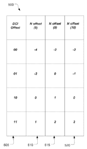
odd values. Figure 5 depicts exemplary n offset values 500 for embodiments
containing a
- 8 -
CA 02871105 2014-10-20
WO 2013/180935
PCT/US2013/040614
combination of even and odd values. Similarly to Figures 3 and 4, the
discussed
n offset values may be the ARI values discussed above. In Figure 5, an eighth
set of
n offset values 510 may correspond to the set of values 505 signaled on the
DCI in an eighth
embodiment. For example, an n offset of -4, -2, 0, or 1 may correspond to a
DCI signal of 00,
01, 10, or 11, respectively. A ninth set of noffsetvalues 515 may correspond
to the set of
values 505 signaled on the DCI in a ninth embodiment. For example, an n offset
of -2, 0, 1,
or 2 may correspond to a DCI signal of 00, 01, 10, or 11, respectively. A
tenth set of
n offset values 520 may correspond to the set of values 505 signaled on the
DCI in a tenth
embodiment. For example, an n offset of -2, -1, 0, or 2 may correspond to a
DCI signal of 00,
01, 10, or 11, respectively.
The use of a combination of odd values and even values may be desirable for
several reasons. First, a scaling value may be applied to maximize the
flexibility of the
n offset values. For example, if transmit diversity such as SORTD is not used
in the PUCCH
transmission, then a non-even n offset value may be acceptable. However, if
the PUCCH is
later transmitted using SORTD, then an even n offset value may be desirable. A
combination
of odd and even values may allow for both scenarios, because a scaling factor
such as 2
may be applied so that the odd values become the even values desired for the
SORTD
transmission. As an example and referring to the n offset values 515 of the
ninth
embodiment, the use of a scaling factor such as 2 may make the values (-2, 0,
1, 2)
become the even values (-4, 0, 2, 4). In some embodiments the RRC may
configure the
scaling factor, while in other embodiments the eNB may configure the scaling
factor for
use by the UE for the PUCCH transmission.
In certain embodiments where the ePDCCH is used in a stand-alone new carrier
type (NCT), for example as a PCell, the above described embodiments may be
altered. For
example, the n offset value may be maintained considering possible future
extensions such as
downlink multiuser multiple-input and multiple output (MU-MIMO) or coordinated
multipoint transmission (CoMP). Alternatively, the n offset value may be
effectively
removed, for example by always setting the n offset value to 0. In this
instance the
n offset value may be used as a virtual cyclic redundancy check (CRC) field.
In other
embodiments, the n offset value may be completely removed from the DCI.
-9 -
CA 02871105 2014-10-20
WO 2013/180935
PCT/US2013/040614
As discussed above, in certain embodiments starting offsets for dynamic
resource
allocation may be provided by RRC parameters indicated by RRC signaling. In
those
embodiments, at least one nom
et value may contain at least one of the RRC parameters.
N(l,k)
For example, denoting PUCCH (where k=0, 1) as a UE-specific starting offset
RRC
5Npc=o)
parameter for ePDCCH set k, an n
offset value may contain at least one of PUCCH and/or
ilicc=cik .
The UE specific starting offset values NCH
may help to efficiently use a given
PUCCH resource region by using the RRC parameters in the noffset to offset the
PUCCH
parameters so that physical uplink shared channel (PUSCH) signals may also be
1 0
transmitted in those PUCCH region depending on eNB scheduling.
In these embodiments, the offset values n offset may be 0, 2, N,,1
ilicc=c )õ , ornilicc=c1)õ . In
these embodiments, the noffset parameters may therefore be a hybrid version of
even
number offset values and ePDCCH offset values, as described above. Other
variants for
n offset may include 0, N, nu'kc-c )õ + /14-1, or N(plu'kc=c1)õ+1112 where N,
Ml, and M2 are the
integer values. In this example, N, M1 and M2 may each be equal to 1 or -1. In
some
embodiments all three of the variables may be equal to one another, and in
other
embodiments at least one of the variables may have a value that is different
from the other
variables. In other embodiments, N may be equal to 1 or -1, and M1 and/or M2
may be
equal to O. In certain embodiments, N, Ml, and M2 may be an even number such
as 2, -2,
or some other even number to avoid resource collisions by SORTD or FDD channel
selection. For example, in these embodiments n offset may be 0, 2, ngl)H 2 ,
n'ukc=c1)H 2 where " A" represents +A or -A.
In a certain embodiments, the offset values n offset for an ePDCCH set k may
be 0, 2,
nu'kc=c )1/ ¨ Mplu'k2c7-1, or nu'kc=c1)H ¨ (r. 2
N,lu'kuci, . In these embodiments, the noffset parameters may
therefore effectively change the UE specific starting offset for an ePDCCH set
k into the
signaled n offset value, for example the n offset indicated by ARI as
described above. In other
embodiments, other variants for n offset may include 0, N, nilicc=cc?, ¨
Ar(pliii2,CH M1 1 or
nu'kc=c1)H ¨ N(plu'kuH +1112 where N, Ml, and M2 are integer values. In this
example, N, M1
and M2 may each be equal to 1 or -1. In some embodiments all three of the
variables may
- 10 -
CA 02871105 2014-10-20
WO 2013/180935
PCT/US2013/040614
be equal to one another, and in other embodiments at least one of the
variables may have a
value that is different from the other variables. In other embodiments, N may
be equal to 1
or -1, and M1 and/or M2 may be equal to 0. In certain embodiments, N, Ml, and
M2 may
be an even number such as 2, -2, or some other even number to avoid resource
collisions
n
by SORTD or FDD channel selection. For example, in these embodiments offset
may be 0,
2, nukc=coji_ nu,kccH 2 , u, kc-cl _ N i(olu,kcH 2
where " A" represents +A or -A. In
embodiments where the starting offset for the second ePDCCH set k=1,ni1;c=c1)õ
, is not
configured, the value of nu'kc=c1)õ may be replaced by cell specific starting
offset N-1,1()I
CCH =
In these embodiments, the values of n offset may then be 0, N, nu'kc-c j, ¨
nu'k2vH /1/1, or
NiccH N(plu'k2vH 1112 where N, Ml, and M2 are the integer values.
Embodiments of the present disclosure may be implemented into a system using
any suitable hardware and/or software to configure as desired. Figure 6
schematically
illustrates an example system 600 that may be used to practice various
embodiments
described herein. Figure 6 illustrates, for one embodiment, an example system
600 having
one or more processor(s) 605, system control module 610 coupled to at least
one of the
processor(s) 605, system memory 615 coupled to system control module 610, non-
volatile
memory (NVM)/storage 620 coupled to system control module 610, and one or more
communications interface(s) 625 coupled to system control module 610.
In some embodiments, the system 600 may be capable of functioning as the UE
110 as described herein. In other embodiments, the system 600 may be capable
of
functioning as the eNB 105 depicted in the embodiment shown in Figure 1 or any
one of
the other described embodiments. In some embodiments, the system 600 may
include one
or more computer-readable media (e.g., system memory or NVM/storage 620)
having
instructions and one or more processors (e.g., processor(s) 605) coupled with
the one or
more computer-readable media and configured to execute the instructions to
implement a
module to perform actions described herein.
System control module 610 for one embodiment may include any suitable
interface
controllers to provide for any suitable interface to at least one of the
processor(s) 605
and/or to any suitable device or component in communication with system
control module
610.
System control module 610 may include memory controller module 630 to provide
an interface to system memory 615. The memory controller module 630 may be a
- 11 -
CA 02871105 2014-10-20
WO 2013/180935
PCT/US2013/040614
hardware module, a software module, and/or a firmware module.
System memory 615 may be used to load and store data and/or instructions, for
example, for system 600. System memory 615 for one embodiment may include any
suitable volatile memory, such as suitable DRAM, for example. In some
embodiments, the
system memory 615 may include double data rate type four synchronous dynamic
random-access memory (DDR4 SDRAM).
System control module 610 for one embodiment may include one or more
input/output (I/0) controller(s) to provide an interface to NVM/storage 620
and
communications interface(s) 625.
The NVM/storage 620 may be used to store data and/or instructions, for
example.
NVM/storage 620 may include any suitable non-volatile memory, such as flash
memory,
for example, and/or may include any suitable non-volatile storage device(s),
such as one or
more hard disk drive(s) (HDD(s)), one or more compact disc (CD) drive(s),
and/or one or
more digital versatile disc (DVD) drive(s), for example.
The NVM/storage 620 may include a storage resource physically part of a device
on which the system 600 is installed or it may be accessible by, but not
necessarily a part
of, the device. For example, the NVM/storage 620 may be accessed over a
network via the
communications interface(s) 625.
Communications interface(s) 625 may provide an interface for system 600 to
communicate over one or more network(s) and/or with any other suitable device.
The
system 600 may wirelessly communicate with the one or more components of the
wireless
network in accordance with any of one or more wireless network standards
and/or
protocols. For example, the communications interface(s) 625 may be coupled
with the
transceiver module 120 discussed above with respect to Figure 1.
For one embodiment, at least one of the processor(s) 605 may be packaged
together with logic for one or more controller(s) of system control module
610, e.g.,
memory controller module 630. For one embodiment, at least one of the
processor(s) 605
may be packaged together with logic for one or more controllers of system
control module
610 to form a System in Package (SiP). For one embodiment, at least one of the
processor(s) 605 may be integrated on the same die with logic for one or more
controller(s) of system control module 610. For one embodiment, at least one
of the
processor(s) 605 may be integrated on the same die with logic for one or more
controller(s) of system control module 610 to form a System on Chip (SoC).
In various embodiments, the system 600 may be, but is not limited to, a
server, a
- 12 -
CA 02871105 2014-10-20
WO 2013/180935
PCT/US2013/040614
workstation, a desktop computing device, or a mobile computing device (e.g., a
laptop
computing device, a handheld computing device, a tablet, a netbook, etc.). In
various
embodiments, the system 600 may have more or less components, and/or different
architectures. For example, in some embodiments, the system 600 includes one
or more of
a camera, a keyboard, liquid crystal display (LCD) screen (including touch
screen
displays), non-volatile memory port, multiple antennas, graphics chip,
application-specific
integrated circuit (ASIC), and speakers.
Methods and apparatuses are provided herein for dynamically allocating uplink
control channel resources. In certain embodiments, UE circuitry may be to
receive an
indication of an offset value on an ePDCCH. The UE circuitry may further
receive one or
more eCCEs of the ePDCCH. The UE circuitry may then select, based on the
indication of
the offset value, an offset value from a table comprising a plurality of
stored offset values,
the plurality of stored offset values comprising offset values of -2, -1, 0,
and 2. Then, the
UE circuitry may determine allocation of an uplink resource of a PUCCH based
at least in
part on an index of a first eCCE of the one or more eCCEs and the selected
offset value. In
certain embodiments the indication of the offset value may be received in
downlink
control information transmitted in the ePDCCH, while in other embodiments the
offset
value may be based at least in part on an antenna port associated with the
ePDCCH. In at
least one embodiment the antenna port may be allocated to the first eCCE. In
some
embodiments the allocation of the uplink resource may be based at least in
part on a UE
specific starting offset value for a set of the ePDCCH. Additionally the
offset value may
be based on the UE specific starting offset value or a cell specific starting
offset value. In
some embodiments at least one of the plurality of offset values may be even or
negative,
and a scaling factor may be used to multiply the offset value. Additionally,
the index of
the first eCCE may be less than an index of other eCCEs of the one or more
eCCEs. In
some embodiments, the UE circuitry may be coupled with a graphics chip.
Certain embodiments may further include a UE with receiving and processing
circuitry to perform functions similar to the embodiments described above.
Specifically,
the receiving circuitry may be to monitor an ePDCCH for an offset value of 2,
and obtain
one or more eCCEs of the ePDCCH. Additionally, the receiving circuitry may be
to obtain
one or more CCEs of a PDCCH, and the processing circuitry may be to determine
a first
allocation of an uplink resource of a PUCCH based at least in part on an index
of a first
eCCE of the one or more eCCEs and the offset value, and determine a second
allocation of
an uplink resource of the PUCCH based at least in part on an index of a first
CCE of the
- 13 -
CA 02871105 2014-10-20
WO 2013/180935
PCT/US2013/040614
one or more CCEs. In some embodiments the first allocation and the second
allocation
may be different from one another. In some embodiments, the offset value may
be
signaled in downlink control information in the ePDCCH. In some embodiments,
the
processing circuitry may be to determine the first allocationb ased at least
in part on a
result of the offset value multiplied by a scaling factor. In some
embodiments, the index of
the first eCCE may be less than an index of other eCCEs of the one or more
eCCEs. In
some embodiments, the processing circuitry may be to determine the first
allocation of the
uplink resource based at least in part on a starting offset value for a set of
the ePDCCH
selected from a plurality of sets of the ePDCCH. In some embodiments, the
starting offset
value may be a starting offset value specific to the UE. In some embodiments,
the offset
value may be based at least in part on the starting offset value or a starting
offset value
specific to a cell. In some embodiments, the offset value of 2 may be selected
from the set
consisting of -2, -1, 0, and 2.
Other embodiments may include a UE comprising a receiver to receive an offset
value of 2, and one or more eCCEs of the ePDCCH. The UE may further comprise a
processor coupled with the receiver to allocate an uplink resource of a PUCCH
based at
least in part on an index of a first eCCE of the one or more eCCEs and the
offset value.
The UE may also comprise a transmitter configured to transmit a signal on the
physical
uplink control channel using the first uplink resource. In embodiments, the
receiver may
be to receive the offset value in downlink control information of the ePDCCH.
In
embodiments, the process may be to allocate the uplink resource based at least
in part on
the offset value as multiplied by a scaling factor. In embodiments, the index
of the first
eCCE is less than an index of other eCCEs of the one or more eCCEs. In
embodiments,
the processor may be to allocate the uplink resource based at least in part on
a starting
offset value for a set of the ePDCCH. In embodiments, the starting offset
value is specific
to the UE. In embodiments, the offset value is based at least in part on the
starting offset
value or on a starting offset value specific to a cell. In embodiments, the
offset value of 2
is selected from the set consisting of -2, -1, 0, and 2. In embodiments, a
display may be
coupled with the processor.
Although certain embodiments have been illustrated and described herein for
purposes of description, this application is intended to cover any adaptations
or variations
of the embodiments discussed herein. Therefore, it is manifestly intended that
embodiments described herein be limited only by the claims.
Where the disclosure recites "a" or "a first" element or the equivalent
thereof, such
- 14 -
CA 02871105 2014-10-20
WO 2013/180935
PCT/US2013/040614
disclosure includes one or more such elements, neither requiring nor excluding
two or
more such elements. Further, ordinal indicators (e.g., first, second or third)
for identified
elements are used to distinguish between the elements, and do not indicate or
imply a
required or limited number of such elements, nor do they indicate a particular
position or
order of such elements unless otherwise specifically stated.
- 15 -