Note: Descriptions are shown in the official language in which they were submitted.
CA 02871285 2015-01-30
A SMART PACKAGE AND MONITORING SYSTEM WITH INDICATOR AND
METHOD OF MAKING SAME
Technical Field
The present invention relates to a content use monitoring package with a
status indicator
and a method of making the same.
BACKGROUND INFORMATION
Allan Wilson, Michael Petersen, Ehrensvaerd Jakob and Grip Stina, amongst
others,
have described devices for monitoring, recording and downloading medication
dispensing
histories for blister packaged medication; see for example U.S. Patent Nos.
7,113,101,
7,178,417, 6,628,199, 6,244,462, 7,170,409, 6,616,035, 7,616,116 and 7,772,974
along with
PCT application having publication number WO/2009/135283. Also see Canadian
application
No. 2353350 and U.S. Publication Nos. 20070278285, 20080191174 and
20080053222.
Such devices broadly comprise sensor detecting/monitoring electronic tags,
sensor grids
printed with conductive ink, means of connecting the two and means of
inserting the device in a
pharmaceutical blister package.
Despite having been marketed and tested for ten years, the success of any
current
technology for medication monitoring of blister packages has been severely
limited. A need has
been identified for further refinements of such devices to address problems
with the current
technologies. These include:
= difficulty connecting the flexible substrate grid physically and
electrically to the rigid tag
1
CA 02871285 2014-10-23
WO 2013/159198
PCT/CA2013/000406
= instability of conductive inks printed on paperboard substrates yielding
unreliable
electrical characteristics
= tendency of printed conductive inks to crack under repeated deformation
(bending)
= cost of conductive inks
= difficulty tearing or breaking the substrate with normal tablet expulsion
= cost of the sensor monitoring tag
The pharmaceutical market wants a medication monitoring device that is:
= cheap
= 100 percent reliable
= fits seamlessly into the packaging process
= is easy for the consumer to use
= has a reusable electronic module
= allows for the use of breakable substrates to facilitate consumer use
= allows for the use of thin substrates to minimize package bulk
= can accommodate optional functionality including reminders, data input
buttons, and
LED and LCD displays, etc.
2
CA 02871285 2014-10-23
WO 2013/159198
PCT/CA2013/000406
= can accommodate optional printed devices including humidity and
temperature sensors,
printed wireless communication including capacitive coupled, RFID, HF, UHF,
Bluetooth
and NFC, and OLED displays, printed batteries etc
Furthermore, the Clinical Trials sector in Pharmaceutical Business requires
= very fast turn-around
= minimal tooling cost and delays
= small volume runs which can be produced reliably and to pharmaceutical
standards
= seamless integration into clinical trials packaging process and using
standard
pharmaceutical child resistant packaging solutions such as DosePak (by
Meadwestvaco), Eco-SlideRX (by Keystone Packaging), SHR (by Stora Enso) and
any
other type of blister card solution existing now or in the future.
SUMMARY
In accordance with one aspect of the present invention, there is provided a
smart
package monitoring system comprising an electronic sensor monitoring tag
having re-usable
electronic circuitry and power source; a conductive grid printed on a thin
flexible substrate and
connected to the tag so the tag and grid are in electrical continuity to form
a monitoring device;
and an optical ink indicator configured to display the status of the package.
In accordance with another aspect of the present invention, there is provided
the smart
package monitoring system wherein the conductive grid is aligned with an
opening of the smart
package.
In accordance with a further aspect of the present invention, there is
provided the smart
package monitoring system wherein the conductive grid is aligned with an
opening of the smart
package.
In accordance with yet a further aspect of the present invention, there is
provided the
smart package monitoring system wherein the conductive grid is aligned with an
opening of the
smart package.
3
CA 02871285 2014-10-23
WO 2013/159198 PCT/CA2013/000406
In accordance with a still further aspect of the present invention, there is
provided the
smart package monitoring system wherein the optical ink indicator is
associated with the
conductive grid.
In accordance with yet another aspect of the present invention, there is
provided the
smart package monitoring system wherein the optical ink indicator is formed
from bistatic inks.
In accordance with another aspect of the present invention, there is provided
the smart
package monitoring system wherein the optical ink indicator is formed from
printed OLED or an
LED module.
In accordance with a further aspect of the present invention, there is
provided the smart
package monitoring system wherein the status is indicated with a change in
color.
In accordance with yet a further aspect of the present invention, there is
provided the
smart package monitoring system wherein the status indicates the package being
unopened,
the package being opened within an appropriate time window, the package being
opened within
an inappropriate time window, and/or expiration of content by means of time,
temperature,
humidity sensor, exposure to UV radiation or non-compliancy.
In accordance with a still further aspect of the present invention, there is
provided a
smart package monitoring system comprising an electronic sensor monitoring tag
having re-
usable electronic circuitry and power source; a conductive grid printed on a
thin flexible
substrate; and a multiplexer connecting the tag to the conductive grid so the
tag and grid are in
electrical continuity to form a monitoring device.
In accordance with yet another aspect of the present invention, there is
provided the
smart package monitoring system wherein the conductive grid is aligned with an
opening of the
smart package.
In accordance with another aspect of the present invention, there is provided
the smart
package monitoring system wherein the multiplexer is formed of printed
transistors.
4
CA 02871285 2014-10-23
WO 2013/159198 PCT/CA2013/000406
In accordance with a further aspect of the present invention, there is
provided the smart
package monitoring system wherein the multiplexer is printed with the
conductive grid.
In accordance with yet a further aspect of the present invention, there is
provided the
smart package monitoring system wherein the multiplexer connects the grid to
the tag with at
least two leads.
In accordance with a still further aspect of the present invention, there is
provided a
smart package comprising the smart package monitoring system and a card having
product
receptacles.
In accordance with yet another aspect of the present invention, there is
provided the
smart package wherein the product receptacles are blisters.
In accordance with another aspect of the present invention, there is provided
a smart
package comprising a card having product receptacles and a conductive side; an
electronic
sensor monitoring tag having re-usable electronic circuitry and power source;
and a conductive
grid printed on a thin flexible substrate and connected to the tag so the tag
and grid are in
electrical continuity to form a monitoring device; wherein the conductive grid
includes capacitive
sensors formed with the conductive side of the card as one of the plates of
the capacitive
sensors; and wherein the conductive grid is aligned with the product
receptacles in the card.
In accordance with a further aspect of the present invention, there is
provided the smart
package wherein each of the capacitive sensors has the other plate formed on a
thin plastic
layer and positioned so as to form a capacitive element with the conductive
side of the card.
In accordance with yet a further aspect of the present invention, there is
provided the
smart package wherein each capacitive element is of variable size.
In accordance with a still further aspect of the present invention, there is
provided the
smart package further comprising a conductive trace grid associated with the
capacitive sensors
in the conductive grid.
CA 02871285 2014-10-23
WO 2013/159198
PCT/CA2013/000406
In accordance with yet another aspect of the present invention, there is
provided the
smart package wherein the grid is connected using conductive patches applied
or printed onto
heat sealable cardboard.
In accordance with another aspect of the present invention, there is provided
the smart
package wherein the grid is connected using conductive stitching.
In accordance with a further aspect of the present invention, there is
provided the smart
package wherein the grid is connected using a continuous surface of Z-
directional conductive
adhesive tape.
In accordance with yet a further aspect of the present invention, there is
provided the
smart package wherein the grid is connected using selectively applied XYZ-
directional
conductive adhesive tape.
In accordance with a still further aspect of the present invention, there is
provided the
smart package wherein the grid is connected using a continuous surface of
anisotropic
conductive film.
In accordance with yet another aspect of the present invention, there is
provided the
smart package wherein the grid is formed with thermal transfer ribbon digital
printing
technology.
In accordance with another aspect of the present invention, there is provided
the smart
package wherein the grid is formed with vacuum deposition.
In accordance with a further aspect of the present invention, there is
provided the smart
package wherein the product receptacles are blisters.
In accordance with yet a further aspect of the present invention, there is
provided a
method of forming a conductive grid having a substrate for a smart package
comprising the
steps of releasing conductive material from a continuous roll of conductively
coated transfer
6
CA 02871285 2014-10-23
WO 2013/159198
PCT/CA2013/000406
ribbon onto a surface of the substrate and thereby subtractively forming
sensor grids and
connection patches to be joined with an electronic tag of the smart package.
In accordance with a still further aspect of the present invention, there is
provided the
method further comprising the step of applying a heat activated adhesive to
one side of the grid.
In accordance with yet another aspect of the present invention, there is
provided the
smart package for use in monitoring patient compliance during clinical drug
trials.
In accordance with another aspect of the present invention, there is provided
the smart
package wherein the tag has data communication means for transmitting data.
In accordance with a further aspect of the present invention, there is
provided the smart
package wherein the data is used for measuring time-dependent covariates to
reduce error
variance and increase statistical power of the drug trial.
In accordance with yet a further aspect of the present invention, there is
provided the
smart package wherein the data establishes patient compliance profiles.
In accordance with a still further aspect of the present invention, there is
provided the
smart package wherein the patient compliance profiles incorporate a time
dimension using
multivariate regression techniques to create dynamic compliance profiles for
individual patients
or groups of patients.
In accordance with yet another aspect of the present invention, there is
provided the
smart package wherein the data is from various sources and is pooled to form a
common
resource for further data mining.
In accordance with another aspect of the present invention, there is provided
the smart
package wherein the pooled data are stored remotely on a cloud server.
7
CA 02871285 2014-10-23
WO 2013/159198
PCT/CA2013/000406
In accordance with a further aspect of the present invention, there is
provided the smart
package used as a secure compliance monitoring blister package for the
dispensing of
medication.
In accordance with yet a further aspect of the present invention, there is
provided the
smart package wherein the blister package incorporates a unique ID number to
facilitate
tracking.
In accordance with a still further aspect of the present invention, there is
provided the
smart package wherein the ID number is used to authenticate the content and
detect tampering
with the package.
In accordance with yet another aspect of the present invention, there is
provided the
smart package wherein the package is equipped with reminder devices for the
user.
In accordance with another aspect of the present invention, there is provided
the smart
package wherein the reminders are auditory, visual or tactile using sounds,
LEDs, LCDs,
OLEDs or vibration.
In accordance with a further aspect of the present invention, there is
provided the smart
package monitoring system wherein the tag validates suitability of the content
based on pre-set
thresholds.
In accordance with yet a further aspect of the present invention, there is
provided the
smart package wherein the optical ink indicator changes color to indicate that
the content shall
not be consumed when the tag determines the content is unsuitable based on the
pre-set
thresholds.
BRIEF DESCRIPTION OF THE DRAWINGS
The invention will be further understood from the following description with
reference to
the attached drawings.
8
CA 02871285 2014-10-23
WO 2013/159198 PCT/CA2013/000406
Figure 1 shows the content use monitoring package in a disassembled state,
showing
each layer therein;
Figure 2A shows printing of the conductive grid with an additive printing
process, or
application using vacuum metal vapour deposition technology;
Figures 2B shows printing of the conductive grid with a subtractive printing
process;
Figure 3 depicts die-cutting the printed grid to create the interface with one
part of the
flat flex connector;
Figure 4 shows optional printed functions that can be accommodated because of
the
space savings resulting from the more accurate printing of the conductive
grid;
Figure 5 shows the connection of tag and grid by flat flex connector;
Figure 6A shows the finished package in an open state after heat or cold
sealing;
Figure 6B shows the finished package in a closed state with the unique die-cut
spine;
Figure 7 shows hard wired and wireless communication of data from the package
to
computers, PDAs and data storage devices; and
Figure 8 shows means of recycling the tag after the package has been used.
Figure 9 shows a content use monitoring package and the printed circuitry.
Figure 10 shows a flow chart of operation for the indicator status.
Figure 11 shows circuitry and how the battery can be connected to every
module.
Figure 12 shows a multiplexer that can be used between the tag and the sensor.
Figure 13 shows a grid cable inserted into the connector.
Figure 14 shows a smart label indicator on the back of the package.
Figure 15 shows assembly of the package.
Figure 16 shows assembly of the finished product.
Figure 17 shows thermal transfer printing.
Figure 18 shows a connective trace being broken.
Figure 19 shows thermal transfer printing on a resistance based grid. A
capacitive grid
could also be similarly used.
Figure 20 shows a capacitive singular dose detection, printing both plates.
Figure 21 shows a capacitive grid, printing 1 plate, where the 2nd plate is
from the blister
foil itself. This is for a generic grid design where each dose is the same.
i.e. it cannot
differentiate between doses.
Figure 22 shows a capacitive grid, printing 1 plate, the 2nd plate is from the
blister
9
CA 02871285 2015-01-30
foil itself. This is for a specific grid design where each dose is NOT the
same. i.e. it can
differentiate between doses.
Figure 23 shows a multilayer circuit.
Figure 24 shows use of XYZ tape for connecting the tag to the grid.
Figure 25 shows use of Z-tape for connecting the tag to the grid.
Figure 26 shows use of anisotropic conductive film for connecting the tag to
the grid.
Figure 27 shows assembly of the package with Mylar; it is a Med-ic insert
built as a
pharmaceutical/commercial package.
Figure 28 shows a Med-ic insert Clinical Trial (Child resistant (CR) ready).
Figure 29 shows a Med-ic Insert in actual Clinical Trial CR packaging.
Figure 30 shows grid manufacturing using vacuum deposition.
Figure 31A shows tag/grid connection using conductive ink/heat activated
adhesive with
the ink under the adhesive.
Figure 31B shows tag/grid connection using conductive ink/heat activated
adhesive with
the ink above the adhesive.
DETAILED DESCRIPTION
The invention uses technology discussed in Canadian Application No. 2,719,054.
Initially Figures 1 to 8 will be discussed in order to describe an example of
a content use
monitoring package and method of manufacturing thereof. This particular
example is shown
within the context of monitoring the consumption of blister-packaged
medication doses; however
it will be appreciated that other shapes, sizes and types of packages
containing other types of
contents could also be monitored.
Figure 1 shows the various layers of an example of a content use monitoring
package.
The cover 10 or top layer is preferably made of Easy Seal paperboard or
similar material
commonly used in the food and pharmaceutical packaging industry. This is
followed by a
medication blister card 12 underneath with each blister aligned with a cutout
20 in the cover 10.
The third layer comprises a reusable electronic sensor monitoring tag 14
connected to a
conductive grid 16 printed on thin Mylar, plastic or similar substrate by a
flat flex connector 26
which connection is reversible by unplugging. The grid 16 is rupturable and is
aligned with the
CA 02871285 2014-10-23
WO 2013/159198 PCT/CA2013/000406
associated blisters and may or may not contain a self-adhesive layer with
removable liner. The
fourth and bottom layer is a backing made of Easy Seal or other paperboard
die cut to form a
pull-out tab 18 to tear open the used package and allow the tag 14 to be
removed from the
package by unplugging the connector 26. The tag 14 can then be reused in
conjunction with a
new printed grid and its battery replaced as required. The backing has cutouts
21 associated
with the cut-outs 20 in the cover 10. The conductive grid can be optionally
adhered to the blister
card with any form of suitable self-adhesive means.
Figure 2A shows one manner of printing the conductive grid by an additive
printing
process using conductive inks containing zinc, silver, aluminium, carbon or
other conductive
material. This can be accomplished using standard flexographic, screenprint,
inkjet, offset, or
other printing methods. Also shown in Figure 28 is the subtractive printing
process in which the
dielectric Mylar or similar substrate has been coated with a conductive
substance that is
subsequently removed by die-cutting or chemical etching to leave behind the
conductive traces
of the grid. It is also possible to produce a subtractive process by die
cutting thin flexible foils
and applying them onto a dielectric surface.
Figure 3 shows how the grid contacts for a flat flex connector can be die-cut
from the
printed grid for precise alignment with the contacts of the connector. Precise
alignment is
important if numerous conductive traces are to be connected to the tag as in
digital grid designs
having many individual circuits. The flat cable wires 30 for the flat flex
connector are die-cut
from the grid inlay as shown in the expanded view. The grid inlay is also die-
cut to create flat
connector wires along with the blister opening pattern and to ensure a fit
with the paperboard.
In Figure 4 a number of optional printed functions are shown that are made
possible by
the increased empty space on the grid substrate due to the decreased area
required for the
more accurately printed die-cut conductive traces. For example, areas can be
allotted to an
organic LED (OLED) display 40, a printed input button 42 for users to input
data to the tag (such
as a self-adhesive metal dome button 43), a printed battery 44, printed
humidity sensors 46,
printed or applied temperature sensors 48, and a variety of communication
modes 50 including
Capacitive Coupled, RFID, HF, UHF, Bluetooth, GSM and NFC. Use of a battery
printed on the
grid allows for a smaller tag, further contributing to cost savings and ease
of inserting the
monitoring device into existing assembly processes. Some printed batteries can
take on
11
CA 02871285 2014-10-23
WO 2013/159198 PCT/CA2013/000406
organic shapes, fitting themselves into available open space, rather than
requiring a particular
geometric area. If an OLED display 40 is provided, the cover 10 will have a
window 24 to view
the display (Figure 1).
Figure 5 shows a means of connecting the sensor monitoring tag 14 to the
printed grid
16 using a two-part reversible flat flex connector 26. The tag 14 has a
microchip 52 and
protective foam 54. Other optional components include an on-board temperature
sensor 56, on-
board humidity sensor 58 or indicator LEDs 60. The tag 14 can also optionally
include wired
communication 62 such as a micro-B USB plug.
In Figure 6A a completed medication compliance package 68 is shown in an open
state
with the monitoring device (tag connected to grid) and the medication blister
card hot 64 or cold
66 sealed between two layers of paperboard. Figure 6B shows two instances of
the medication
package in a closed state and one location of the pull-out 70 for tag removal.
The spine 72 is
rounded by die-cutting so the printed conductive traces 74 bend smoothly
across the spine 72
and are less likely to be damaged by opening and closing cycles.
Figure 7 shows both hard-wired and wireless means by which the data from the
tag can
be transmitted to computers, PDAs, data servers or the cloud or other such
network conferring
great flexibility of use on the device. The wired communication port 62 can be
used to connect
for example by USB 76 to computer. Wireless communication means include
Capacitive
Coupled, RFID, HF, UHF, Bluetooth and NFC. Other wired and wireless means are
possible.
Figure 8 shows removal of the tag from the used package by opening the pull-
tab and
unplugging the flat flex connector. The tag is then recycled, refurbished if
required by adding a
new power source, reprogrammed if required and attached to a new conductive
grid to be
inserted in a new package. The grid and paperboard are disposable. Figure 8
also shows in
expanded view how an event is triggered when the conductive trace is broken
and the
medication is pushed through the blister. See also Figure 18 for a close-up of
the connectivity
being broken 140.
Ultra thin (e.g.: MylarTm, food grade plastic, etc.) printed grid substrates
can be used to
facilitate consumer use by easy and predictable breaking of the substrate and
conductive grid
12
CA 02871285 2014-10-23
WO 2013/159198 PCT/CA2013/000406
by tablet expulsions from the associated blister. Such non paperboard
substrates are humidity
stable and give more reliable electrical characteristics to the printed grid,
minimizing false or
missed expulsion events. Thin substrates are easily attached to the blister
card (usually by use
of self-adhesive backing), and also contribute to easy consumer use by
minimizing package
thickness.
Figure 9 shows a content use monitoring package and associated printed
circuitry.
Again, while the context of the example of figure 9 is with respect to a
blister card containing
medicine, other applications are envisioned for other types of packaging
containing other
contents.
The standard blister package of Figure 9 has a little patch of bistatic
current-sensitive
color-change material beside or around each blister. The color state of such
patch shows the
dosing status of the associated dose. In the example shown in Figure 9, the
color green 80
indicates a start point that is active at zero hours. The color white 82
indicates inactive. The
battery 84 is shown printed in the exposed view of the printed inlay and an
exploded view shows
a flowchart of the printed inlay. The flowchart shows an optical ink indicator
surrounding each
blister in conjunction with the printed electronic grid. It will be noted that
other colors besides
green and white could be used. The electronic module applied to the package
can track
anticipated expiration of the content by means of time and temperature and/or
humidity sensor
and thereby also validate the suitability of the contents of the package
depending on pre-set
thresholds. The thresholds can cause the printed static OLED color patches to
turn a specific
color so as to indicate that further doses from the package shall not be
consumed. Excessive
expose to UV radiation can also be monitored and displayed. Furthermore,
status could be
reflective of the package as a whole and not just for each dose.
Figure 10 shows a flow chart of operation for the indicator status of Figure
9. In A the
initial packet is started when the seal is broken. In B the pill is taken
within the appropriate time
window and the status indicator is green. In C the pill is taken outside the
time window and the
status indicator in this example is red. For those pills that have not been
opened, the status
indicator is white.
13
CA 02871285 2014-10-23
WO 2013/159198 PCT/CA2013/000406
Figure 11 shows sample circuitry for the system of Figure 9 and also shows
connection
of the battery to every module. The battery can be replaced as required,
increasing the number
of reuses of the tag. The tag's firmware can optionally contain an algorithm
to track battery
usage and indicate when replacement is required.
Figure 12 shows an optional multiplexer 86 that is used between the tag 14 and
the grid
sensor 88. Printed transistors can be used as multiplexers to reduce the
number of traces
required to the main chip. The multiplexer allows detection of a large number
of doses while
keeping the connections between the tag and grid to a minimum. The multiplexer
while working
with tag logic resides preferably on the grid. This allows for grids with a
large content/product
count to be monitored by a tag with a much smaller tag to grid connection
count. With n tag/grid
connections the multiplexer will enable 2n product receptacles on the grid to
be monitored.
Used in the above example of Figure 9, n tag/grid connections enables 2n doses
on the grid to
be monitored.
In place of zero insertion force (ZIF) or low-insertion force connectors,
transistors can be
printed on the same substrate as the traces which can be arranged to act as a
multi-plexing
circuit. Such an arrangement only takes a few hundred transistors. The
advantage is that it
reduces the number of connections. For example, a 100-receptacle package could
be arranged
in a 10x10 printed grid requiring only 10 connections to the electronic tag.
This makes it both
less expensive and easier to connect the printed trace circuit to the
electronic tag module as
well as allowing the monitoring of far more product receptacles on the package
than the actual
tag integrated circuit has inputs for connection.
Figure 13 shows a grid cable 90 inserted into the connector, with a small
exploded view
showing the same.
Figure 14 shows a smart label indicator that can be placed on the package,
preferably
on the back of the package. The smart label can be used to monitor and report
various events,
such as the detection of radioactivity, the activation of a timer, spoilage or
the occurrence of a
freeze event. Various symbols, icon indicators 98 and/or text 100 can be used
to describe the
events. A timer indicator 104 can be included or a temperature indicator 102.
In the sample
14
CA 02871285 2014-10-23
WO 2013/159198 PCT/CA2013/000406
timer indicator 104 the time progress black bar fades to white. The various
layers in the smart
label are shown and include an electrode 94 and film 96.
Figure 15 shows one manner of assembling the package. First the liner 106 is
peeled
away to expose the adhesive backing. Then the inlay 108 is placed face up on
the alignment
markers. Adhesive foil 110 is placed over the inlay to isolate the contents of
the product
receptacles. Paperboard flap A is folded over flap B to conceal the tag and
traces. The flaps
112 can then be cold sealed or heat sealed together, see for example Figure 6.
Figure 27 shows another manner of assembling the package using Mylar. At 172 a
first
Mylar strip is added over the paperboard spine and a second Mylar strip is
added over thick
trace of the inlay. At 174 the liner is peeled exposing an adhesive backing.
At 176 an inlay is
placed face up on alignment markers. At 178 adhesive foil is placed over the
inlay to isolate the
contents of the product receptacles. At 180 paperboard flap A is folded over
paperboard flap B
to conceal tag and traces. The flaps can then be cold sealed or heat sealed
together.
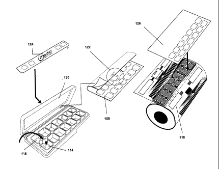
Figure 16 shows one manner of assembling the finished product. First the
medication or
desired contents 114 are placed into the product receptacles, which in this
example are
polypropylene casing slots 116. The adhesive liner 106 is then removed from
the inlay and the
inlay 108 is aligned over the slots. There is no adhesive over the slot area.
The ECM tag or
printed electronics and the optical ink indicators 118 are folded over and
attached to the casing
cover 120. A copper trace cover label 126 covers the printed electronics and
the optical ink
indicators 118. Magnetic sensors 122 can be used to detect the opening or
closing of the case.
A branding label 124 can be applied to the spine.
Various forms of optical ink indicators can be used. For example, bistatic
inks can be
used, which have advantages over printed OLED and LED modules since bistatic
inks do not
require power to maintain color.
The substrate can be a full printed Mylar substrate circuit culminating into a
printed zero
insertion force (ZIF) connection. This circuit can be used in reverse by
controlling printed
display patches around or beside the individual product receptacle areas.
CA 02871285 2014-10-23
WO 2013/159198 PCT/CA2013/000406
The conductive traces on Mylar or some other inert substrate with each line
leading back
to the tag can be used for a second purpose of powering small display patches
beside or
around each product receptacle or on pre-defined areas of the package. With
some printable
inks, the state of so-called bi-static display modules can be changed by
running a current
through the inks. Some e-readers in the market currently achieve that on black
and white
displays, such as E-ink used on the Kindle readers. These are usually made of
a polymer or
chemical that changes color when electrically charged.
In one embodiment, a display patch is electrically charged through a
corresponding trace
and thus the color is changed from clear (none) to black, or into green,
orange, or red, for
example, indicating, for example in the instance that the product receptacles
contain
medication, that a particular dose is ready to be taken, is overdue, has been
skipped or was
taken outside the acceptable dose window. Even once the trace has been broken,
the color for
that particular area remains stable and unchanged, giving an instant overview
of dosing
compliance without the need to scan and download the data from the package.
Such bi-static
patches can be associated with individual doses, or be otherwise arranged so
as to provide a
simple adherence overview of the package use.
Removing the tag does not change the color. The status indicator complements
re-
usable electronics as the tag can be used within another package, but the
existing package
without any electronics still provides a visual overview of the product
receptacle statuses, which
could include patient dosing history in the instance of medication.
A person of skill in the art will appreciate that this technology can be used
to monitor any
type of packaging and is not strictly limited to medication monitoring. For
example, any package
that can be sealed can include the present invention to monitor the opening of
the package,
along with temperature, time and other similar elements such as shown in
Figure 14. Boxes or
cases can be monitored and the results displayed relating to whether the
contents therein have
spoiled based on elapsed time, exposed temperature, exposed humidity, UV
radiation, shock or
other elements for which is it desired to monitor.
Now will follow a specific example embodiment of the present invention used to
measure
and record patient dosing compliance in the particular case that the product
receptacles contain
16
CA 02871285 2014-10-23
WO 2013/159198 PCT/CA2013/000406
blistered medication. This example serves to illustrate various aspects of the
invention and
methods of manufacturing thereof. It will be appreciated by one skilled in the
art that the
techniques, elements and methods discussed below can be applied to other forms
of packaging
with different contents.
In this example, called the Med-ic system, two core components are included,
the Med-
ic Tag (tag) and Med-ic Grid (grid). The grid is the dose removal sensor while
the tag
interfaces with the grid sensor detecting the dose events and recording the
dose events. The
tag and grid are combined to form a Med-ic Inlay (inlay). The inlay is adhered
to the foil side of
a medication blister. When a dose is removed the dose breaks through a grid
circuit which the
tag filters, detects and records. The inlay and blistered medication are
finally sealed together
into a Med-ic Package (package). The package may be heat seal board, pressure
seal board or
a plastic housing. The package protects the inlay/blaster assembly from the
external
environment yet still allows for the easy removal of blistered doses.
The inlay interfaces with an external infrastructure to allow the end user to
better obtain
and view the recorded dose events. The infrastructure can be roughly divided
in two types,
desktop/PC and mobile.
Desktop/PC infrastructure can include a Med-ic Certiscan Desktop Reader
(reader) and
the Med-ic Certiscan (software). The reader, which may be a RFID, NFC or Blue
tooth device
(or all of the above), allows the end users to retrieve the data stored on a
tag and allows the end
user to view, manipulate and store that data with the software.
The mobile infrastructure includes a smart phone running a Med-ic Certiscan
Mobile App
(app) and Med-ic Server Backend (backend). The smart phone with the app
combines the
functionality of the reader and software. The smart phone also communicates
with the tag using
RFID, NFC and Blue Tooth but can also use WIFI, GSM and dynamic QR codes.
Dynamic QR
codes allow the smart phone and tag to communicate optically. The smart phone
with either
WIFI or Cellular Wireless Data (wireless) will act as a two-way communication
channel with the
backend. The smart phone and backend together enable Med-ic Cloud (cloud)
based services
for the end user. (At this point it should be noted that a reader may be
enabled with wireless
communication and can communicate with the backend as well) Cloud services
include:
17
CA 02871285 2014-10-23
WO 2013/159198 PCT/CA2013/000406
= Centralized remote tag data storage and backup
= Real time alerts between the end user and a care giver
= Dosing reminders for end user
= End user account management
Med-ic Tag
The tag provides an interface to a Med-ic grid, and the processing power to
detect, filter and
store dose events as well as communicate the presence of dose events to a
reader and host
device capable of greater functionality that may be needed by the end user.
The tag is mostly
manufactured with traditional PCB processes but does allow for functionality
to be moved off
board and implemented with printed electronics. The tag can contain the
following modules:
= A central processor to provide control over the entire tag system
= A time unit module which provides an absolute timestamp to be assigned to
each
detected dose
= A power module that will power the tag for up to 5 years in the field
= A communication module that allows the tags to transmit/upload data to a
reader and
host device
= A sensor connection interface that allows the tag to communicate with the
grid to sense
dose removal
Optionally the grid may contain the following additional modules:
= A display module to show status and reminders to the end user making
communication
with a host device less necessary
= An audio module to indicate both status and reminders to the user
= Additional sensor platforms for detecting and storing temperature,
humidity, acceleration,
impulse and tactile input
= A multiplexer module as described with reference to Figure 12.
= Advanced communication modules allowing the tag to communicate via Blue
Tooth and
NFC which allows the tag to communicate directly with a smart phone
18
CA 02871285 2014-10-23
WO 2013/159198
PCT/CA2013/000406
Module Description
Central This module may be implemented with an ultra-low power, low cost
Processor microcontroller or ASIC. The module should have enough
functionality to implement a filter algorithm to reject false doses that
can be generated on the grid sensor and non-volatile memory to store
the dose events. The module may also have additional memory to
carry on board end-user data. This module is mostly implemented
using traditional semi-conductor processes.
For less complex processing it may also be possible to implement the
central processing using printable electronics. Similar to identifying
the core, basic activities needed then engineering an ASIC the same
can be done using printable electronic logic, memory, timing circuitry
and sensors.
Time Unit This module interfaces with the central processing to allow for
absolute real-time time stamping of doses events. This module can
be implemented using traditional timing circuitry (e.g. quartz crystal).
Power This module powers the central processing module, sensors
modules,
communication modules and other items in the Med-ic package that
require power. The tag is an ultra-low power device powered by coin
cell batteries or by printed batteries such as Power Paper or other
suitable power sources. =
Communication The tag should be able to communicate gathered dosing
information
to a reader and host for the end user to digest. The primary mode of
communication is preferably with a passive RFID/NFC communication
unit. This allows for ultra-low power, low range two-way
communication with a reader and host device. A host device may be
a dedicated desktop/mobile/gate RFID/NFC reader or a smart phone.
This communication module allows for just a few tags to interface with
a host at one time. RFID/NFC requires a loop antenna for
communication. This loop antenna is traditionally placed on the tag's
19
CA 02871285 2014-10-23
WO 2013/159198
PCT/CA2013/000406
PCB but can also be printed on the paper/PET subtracted of the grid
using printable electronic processes and interfaced with the tag.
More advanced communications may be implemented with Blue Tooth
(especially version 4.0 which allows for a low power communication),
WIFI and even wireless GSM or other forms of communication. This
communication module type is active allowing many tags to
communicate with one host and enables much larger communication
ranges.
Sensor This module connects the tag with one of the many possible
sensor
Connection types. Connection with the primary sensor is discussed in detail
below.
The grid sensor connection types can also be used to connect other
sensors which are not onboard the tag PCB. A temperature and
humidity sensor for example can be attached traditionally to the PCB
or using printed electronics printed off board and connected via a grid
connection type.
Display This module may be used by the tag to display status information
and
reminders to the end user. This module may be onboard the PCB
using a traditional TFT LCD display or off board implemented with
printed electronic technologies such as, E-Ink, OLED and bi-static
displays.
The display module can be used to generate dynamic QR codes
which provide an optical communication path with camera enabled
smart phones.
Multiplexer This module allows for grids with a large dose count to be
monitored
by a tag with a much smaller tag to grid connection count. See Figure
14 and associated text.
Audio This module can be implemented both on and off the tag's PCB to
provide the end user with audio status and reminders. The audio is
most commonly generated with an electromechanical or piezoelectric
CA 02871285 2014-10-23
WO 2013/159198
PCT/CA2013/000406
buzzer.
Med-ic Grid Design
Med-ic grid technology can be divided into two general categories, singular
dose (SDD)
detection and bus dose detection (BDD). With SDD there is a single sensor
circuit/switch for
monitoring each dose. With BDD multiple doses can be monitored with one sensor
circuit/switch.
In SDD's simplest form there is a circuit switch trace covering each dose.
When a dose is
removed the trace is broken, the switch is opened and this is sensed by the
tag. The tag
records both the dose removal timestamp and the specific dose that was
removed. SDD
circuits are mainly constructed with a conductive material forming the
individual switch circuits.
SDD's main advantage is that each dose can be detected individually. The main
disadvantage
is that the tag must support a connection for the switch circuit on the grid
which can involve as
many as 40 individual connections. Having an individual circuit for each dose
presents
significant challenges for routing the switch circuits and for overall
robustness as circuit trace
widths and trace separation must be reduced. This is most problematic when the
grid is
developed with printed electronic technology. Figure 20 shows a printed
capacitive sensor grid
formed with printed capacitors 146, carbon/dielectric material 148 and a
substrate 150 using
SDD.
With BDD multiple doses are monitored by a network of resistances and
conductive traces
all connected on a bus. In resistive BDD each dose on the bus has both a
resistive and
conductive element with the conductive element initially electrically shorting
the resistive
element. When a dose is removed the conductive element is broken forcing the
resistance into
the bus circuit. The increase in bus resistance is sensed by the tag which
records the dose
removal time stamp and some typing information about the dose.
With BDD is it not always possible to detect the specific dose that is
removed. Finer type
granularity can be achieved with BDD as the number of bus elements is
increased and the
number of doses per bus is reduced. Also the ability to control the accuracy
and increase the
relative separation of the resistive elements can increase the type detection
granularity.
21
CA 02871285 2014-10-23
WO 2013/159198 PCT/CA2013/000406
In capacitive BDD each dose on the bus has both a capacitive and conductive
element.
When a dose is removed the capacitance of the dose is removed from the circuit
and the overall
capacitance drops by a defined amount. It is this drop in bus capacitance that
is sensed by the
tag which records the dose removal time stamp and some typing information
about the dose.
The capacitance for each dose can be either manufactured using a two layer
grid (one layer for
each capacitor plate) or by using a single layer grid and utilizing the
conductive material in the
medication blister aluminum backing material as the other capacitor plate. In
both cases there
are two parallel metal plates (A) separated by a dielectric (er) of a
thickness (d) which forms the
capacitor.
C = fr ___________________________________
4
Capacitive sensors can be constructed such that one side of the capacitor is
applied
onto a thin plastic layer and positioned so as to form together with the
blister foil of the
pharmaceutical blister a capacitive element. Such capacitive elements can be
of variable size
so as to determine the exact dose position for each tablet to be removed.
Capacitive sensor
grids can be used alone or in combination with conductive trace grids to
provide for flexible
construction of the sensor grid and the maximum number of individual doses to
be detected.
The main advantage of BDD is the reduced number of connections the tag must
support.
Figure 21 shows a capacitive grid, printing one plate, where the second plate
is from the
blister foil itself. This is for a generic grid design where each dose is the
same. i.e. it cannot
differentiate between doses. The die cut for blister opening 151 is shown.
Figure 22 shows a capacitive grid, printing 1 plate, the 2nd plate is from the
blister
foil itself. This is for a specific grid design where each dose is NOT
the same. i.e. it can differentiate between doses.
Figure 23 shows a multilayer circuit formed with a printed conductive 152, a
printed
dielectric 154, a printed conductive or foil of a blister pack 156 and a
substrate 150. This is
22
CA 02871285 2014-10-23
WO 2013/159198 PCT/CA2013/000406
useful when the blister doses are very dense so there is not enough room to
route all lines in
one layer. Lines can be routed in 2 or more layers with lines on top of other
lines separated by
dielectric to prevent shorting between layers.
Although the above describes SDD and BDD separately it is possible to design a
grid
that mixes the two techniques, thereby managing the associated advantages and
disadvantages.
A second aspect of grid design is related to the die cutting of the grid
around the dose
cavities of the medication blister and the circuit traces running over the
cavities. Die cutting can
be used to introduce controlled failure points to assist in pushing the
contents of the package
through the grid to break a circuit switch to detect the event. Die cutting
also provides a means
to control the breaking thus protecting sensitive sections of the grid.
Med-ic Grid Material
The grid can be manufactured with both traditional PCB processes and printable
electronic
technologies or other such technologies. Various methods include: flex PCB,
Kapton,
flexographic printing on paper/PET/blister barrier foil substrate with
conductive, dielectric and
resistive inks, digital inkjet print (optional roll-to-roll) on
paper/PET/blister barrier foil substrate
with conductive, dielectric and resistive inks, screen print (optional roll-to-
roll) on
paper/PET/blister barrier foil substrate with conductive, dielectric and
resistive inks, metal
plating with catalyst inks onto a PET substrate, metal foil stamping (hot and
cold) onto a
PET/blister barrier foil substrate, PET metal foil etching, and metal foil
thermal transfer printing
on PET/blister barrier foil. A blister barrier foil, usually Aluminum, can
allow for the grid sensor
to be implemented without the need of extra component material.
One such manner of production involves metal foil thermal transfer (MFTT)
printing on PET.
Such a method provides a robust metal layer and is useful for multi-layer
designs. MFTT
printing has extremely low tooling costs and uses subtractive manufacturing.
Thermal transfer
ribbon digital printing technology involves releasing conductive material from
a continuous roll of
conductively coated transfer ribbon onto the surface of the grid substrate,
thereby subtractively
forming sensor grids and connection patches to be joined with the electronic
tag. In addition to
conduction materials, resistive and dielectric material can be transferred to
form circuit
23
CA 02871285 2014-10-23
WO 2013/159198 PCT/CA2013/000406
elements. See Figure 17 which shows ribbon 132, which could be aluminum,
dielectric, carbon,
copper or other similar substance, along with substrate 134 being fed into the
print head 130.
On the other side unselected ribbon medium 136 is fed out along with the
substrate containing
selected ribbon medium 138, i.e. the substrate contains selected aluminum,
dielectric, carbon,
copper or other similar substance. Figure 19 shows the result of resistive
thermal transfer
printing. Printed resistors 142 are shown along with an example SMD resistor
144 which is
placed onto the grid.
Another form of manufacture includes vacuum deposition with various metals
onto a
PET/blister barrier foil substrate. Such a technique is designed for high
volume production
allowing relatively fine grid features to be constructed. This is an additive
manufacturing
method. In vacuum deposition the PET substrate is passed by a metal evaporator
within a
vacuum chamber which coats the PET with a metalized film. A stencil is
inserted between the
metal evaporator and the PET substrate to form the circuit design with
metalized film. Figure 30
shows an arrangement of grid manufacturing using vacuum deposition. A
substrate 206 having
conductive printing is shown in a vacuum deposition chamber. A stencil 210 and
metal
evaporators 212 are used in the process to form the conductive grid.
Yet another method of manufacture includes metal plating using catalyst inks.
Such a
method can be done with both flexographic and digital Inkjet. This method
results in very small
tooling costs and allows small volume production. It is relatively inexpensive
as copper can be
used for the conductive material verses silver based inks. A very robust metal
layer results
when done with a flexographic process. This is an additive manufacturing
method.
Med-ic Tag/Grid Connection
The following connection technologies can be used:
= Traditional cable connecters like zero insertion force (ZIF) connectors
or low force
insertion connectors. The tag implements the connector and the grid implements
the
cable portion that is inserted into the connector
= ACF (Anisotropic conductive film). ACF is a z-axis only conductive
material. The ACF is
placed between corresponding connection pads between the tag and the grid and
then
heated using a precise temperature-time-pressure profile. As the ACF cools the
24
CA 02871285 2014-10-23
WO 2013/159198 PCT/CA2013/000406
conductive partials in the ACF from a robust connection between the tag and
grid. This
method scales very well. It is easy to add more connections and the grid is
easy to
manufacture with only low precision die cutting being necessary. Figure 26
shows use
of anisotropic conductive film 160 for connecting the tag to the grid. In one
example, the
anisotropic conductive film 160 is sandwiched between a liner 162 and an ink
pad 164
abutting the inlay 166. Pressure and heat are applied at around 90 C. In
another
example, the anisotropic conductive film 160 is sandwiched between a PCB pad
168
abutting a PCB 170 and an ink pad 164 abutting the inlay 166. Pressure and
heat are
applied at around 195 C.
= Z-Axis tape. The tag implements a grid socket pad with Z-Axis tape. The
grid
implements the corresponding grid socket. The tag and grid are adhered
together to
make the electrical connection. Note that Z-Axis tape can also be manufactured
from
traditional XYZ conduction tape by simply using separate/isolated pieces on
each socket
pad. Both methods should use a die cut conversion process to assemble the
final
adhesive conductive matrix that is first applied to the tag and then to the
tag with
conductive matrix is applied to the grid. See Figure 24 which shows one
example of use
of XYZ tape for connecting the tag to the grid. Figure 25 shows one example of
use of
Z-tape for connecting the tag to the grid.
= Conductive Thread. The tag and grid implement a few connection pads. The
conduction pads are connected with conductive thread, the thread applied with
an
industrial sewing machine.
= Conductive Epoxy. The tag and grid implement connection pads. Epoxy is
applied
either to the tag or grid and the two are adhered together to form the
electrical
connection.
= Heat activate adhesive. Heat activated adhesive works with printed inks
to hold the tag
pads in position against the conductive grid traces and enable electrical
connection
between the tag and grid. The conducting particles in the ink migrate through
the heat
activated adhesive to provide permanent conduction once the adhesive cures.
The ink
layer can be both printed above or below the heat activated adhesive. The heat
activated adhesive can also be anisotropic conductive aiding and providing
electrical
conduction itself between the tag and the grid. Such a method allows for
simple
connections printed on the final package. This method is scalable and
inexpensive to
produce, while being easy to apply using industry standard heat seal plate
equipment.
CA 02871285 2014-10-23
WO 2013/159198 PCT/CA2013/000406
Figure 31A shows tag/grid connection using conductive ink/heat activated
adhesive with
the ink under the adhesive 214. Figure 31B shows tag/grid connection using
conductive
ink/heat activated adhesive with the ink above the adhesive 214. In each
instance a
PCB 216 is on one side, while the substrate 218 is on the other side. The
printed
conductive 220 is applied prior to pressure and heat. After applying pressure
and heat
the heated conductive 222 is sandwiched between the PCB 216 and substrate 218.
= Mechanical Crimping/Clamping/Stappling The tag and grid connection pads
are held in
conductive connection via pressure provided by metal hardware. The connection
process is quick.
=
Med-ic Grid Converting
Grid production is preferably preformed with a roll-to-roll process. This
allows for high
volume production using commonplace machinery. The following aspects of the
grid can use
separate production processes:
= Tag/Grid Connector ¨ Allows the tag to accurately and quickly connect
with the grid. If
the tag has a connector this means very accurate die cutting to ensure the tag
and grid
are properly aligned when connected.
= Grid shape and dose die/kiss cutting ¨ Allow the overall grid to be
punched out from the
roll-to-roll web and to provide the dose die cutting so the dose can be easily
pushed
through the grid.
= Grid "crack n' peel" liner removal ¨ This provides an easy and convenient
method of
removing the grid liner. The liner is on the opposite side of the printed
design covering
the blister adhesive which allows the grid to be easily shipped and processed.
The
"crack n' peel" can be implemented with special die cutting or by selectively
voiding the
adhesive so the liner easily separates from the grid.
= Selective adhesive ¨ Adhesive should not be present around the dose
windows to
provide a transfer of adhesive on the dose before the patient ingests the
medication.
Selective adhesion can be implemented by a die cutting process to cut the
shape
needed then transfer to the grid or by using a flexographic UV cured print on
adhesive.
26
CA 02871285 2014-10-23
WO 2013/159198 PCT/CA2013/000406
The finished inlay should be designed to fit into a final dosing package. Two
factors to
consider are the placement of the grid with respect to the blistered
medication and the position
of the tag in the package.
The grid should be both aligned and laminated to the blistered medication.
Grid lamination
can be done in two ways:
= Pressure sensitive adhesive (PSA) ¨ The grid is manufactured with a PSA
and liner.
The liner is removed during package assembly to expose the PSA to laminate the
grid to
the blistered medication. The PSA can be applied using a converted adhesive or
by
using a "print on" adhesive.
= Heat activated adhesive ¨ The grid is manufactured with a "print on" heat
activated
adhesive which does not need a protective liner and is used in packages that
are heat
sealed. The final lamination of the grid and medication blister happens during
the final
dose package heat seal. This process also allows for the printing or applying
of selective
conductive materials to form the conductive connections between the electronic
module
and the grid.
Grid alignment to the medication blister can be achieved in two general ways:
= Alignment Tool ¨ An external alignment guide tool that aids in laminating
the medication
blister and grid with the correct registration.
= Built-in Package Alignment ¨ The packaging provides a built in medication
blister
alignment panel that correctly holds the blister onto the grid for lamination.
This
alignment panel may be part of the final packaging or may be a removable part
that is
discarded after the grid and blister are laminated.
The position of the tag relative to the grid inside the package can take a few
forms:
= The tag can be connected adjacent to the grid off the medication blister
card.
= The tag can be connected onto (centrally) the grid and be central to the
medication
blister as well.
27
CA 02871285 2014-10-23
WO 2013/159198 PCT/CA2013/000406
= The medication blister can be formed in such a way that when combined
with the grid
the tag connects directly to connector ribbon made from the grid and the
blister itself.
In all above cases the tag along with the grid are sealed inside the dose
packaging. When
the tag is connected adjacent to the grid it can support both single and
multiple panel
packaging. In multiple panel packaging the tag can be on a different panel
than the blistered
medication locating the connections between the tag and grid across the
package spine.
Packages of this type should have extra reinforcement where grid sections
cross the spine.
In a further scenario the grid itself can be used as the barrier material in
the medication
blister. This has the advantage of removing one piece from the overall
assembly.
Med-ic Package
The finished inlay can be placed within a final drug safe packaging and can be
designed
to fit into all major clinical trial and pharmaceutical drug packaging
formats. The insert provides
four attributes:
= A fully constructed inlay which requires no production in final drug
packaging facilities
= Fully ESD protected which ensures final production can ignore all ESD
safety
procedures and equipment
= A built-in alignment apparatus/method that will register the inlay with
the blistered
medication
= Printed graphics and instruction which help the patient use the
medication as prescribed.
For clinical trial packaging the inlay is formed into an insert which is used
by the end
drug packager to construct the final child resistant (CR) drug packaging. The
final drug
packager can insert and seal (heat seal, cold seal or other) the medication
blister into the insert.
The insert then becomes part of the final package. The insert works with major
CR clinical
packaging such as Keystone's Eco-slide and Key-pak, MVVV's Dosepack and Stora
Enso's
SHR.
28
CA 02871285 2014-10-23
WO 2013/159198 PCT/CA2013/000406
The insert when used in pharmaceutical drug packaging provides the full
packaging
solution. The pharmacist, for example, can place and seal (heat seal, cold or
other) the
medication into the insert to produce the final drug package for the customer.
Figure 28 shows a Med-ic insert Clinical Trial (Child resistant (CR) ready).
In step 190 the
inlay is aligned with printed marking lines. In step an ESD label foil is
added, while the blister
added in step 194. Step 196 involves folding the paperboard flap A over flap
B. The flaps may
be cold or heat sealed together.
Figure 29 shows a Med-ic Insert in actual Clinical Trial CR packaging. In step
198 a
DosePak, Inlay is sealed within an inner sleeve. In step 200, ecoslide-RX and
inlay are sealed
within the inner sleeve and rivits A and B added. Step 202 shows a Stora Enso
and Inlay
paperboard attached to the end panel of the inner box. Step 204 shows
insertion into a child
resistant box.
Quality Assurance (QA) can be used to verify the grids are of high quality and
the tag
functionality is fully operational.
The tag at all times can be programmed to know what QA steps it has passed and
what
steps remain to be completed. Thus if a tag is not ready for a certain step,
the software will alert
the QA personnel that the step is not possible.
The tag transmits data that can be applied to measure the outcome as time-
dependent
covariates or by similar means to reduce error variance and increase the
statistical power of the
trial design. The data can be used to establish patient compliance profiles or
in clinical drug
trials. Patient compliance profiles can incorporate a time dimension using
multivariate
regression techniques to create dynamic compliance profiles for individual
patients or groups of
patients. Patient compliance with medication can be monitored in general
pharmacy settings.
Similarly, the compliance data can be used by the prescribing physician or
pharmacist to
improve the patient's compliance using motivational counselling, positive
reinforcement, limit
setting and/or other behavior modifying techniques. The data obtained in
multiple diverse
settings can be pooled to form a common resource for further data mining. Any
such pooled
29
CA 02871285 2014-10-23
WO 2013/159198 PCT/CA2013/000406
data can be stored remotely on a cloud server. Diverse persons of interest can
be allowed
application-specific access to the pooled remote data base.
The device described can be incorporated into a secure compliance monitoring
blister
package for the dispensing of medications for which compliance with dosing is
considered
critical. Medications with high dependence liability such as opiate and
similar analgesics can be
blister packaged and combined with a dispensing strategy comprising
behavioural contracting,
motivational counselling, and targeted education between the patient and
clinician to minimize
the possibility of inadvertent physical dependence through non compliance with
dosing
schedules. The device can also form part of a home care system to monitor and
improve
patient compliance with prescribed medication. The device can also form part
of an integrated
health management system to improve clinical care and provide logistics track
and trace for
medications. Similarly, the device can form part of a proprietary medication
compliance
monitoring / track and trace / and behaviour modification system for
medications that are
critically sensitive to non-compliance.
The device can also form part of a proprietary system to increase medication
persistence or brand persistence.
The blister package can optionally incorporate a unique ID number to
facilitate tracking
and tracing of the medication. The ID number can be used to authenticate the
content and
detect tampering with the medication package.
The package can be equipped with reminder devices for the user. Such reminders
can
be auditory, visual or tactile using sounds, LEDs, LCDs, OLEDs, or vibration.
It will be appreciated by one skilled in the art that variants can exist in
the above-
described material, package layout, application and method of manufacturing.
The specific
examples provided herein relate to a medication monitoring system and method;
however the
materials, methods of application and arrangements of the invention can be
applied to other
types of packaging and contents.
CA 02871285 2014-10-23
WO 2013/159198
PCT/CA2013/000406
The scope of the claims should not be limited by the preferred embodiments set
forth in
the examples given above, but should be given the broadest interpretation
consistent with the
description as a whole.
31