Note: Descriptions are shown in the official language in which they were submitted.
CA 02871655 2014-10-21
WO 2013/163120 PCT/US2013/037695
SENSOR ARRAY
INCORPORATION BY REFERENCE
[0001] The entirety of U.S. Provisional Application Serial No.
61/636,840, filed
on April 23, 2012, is hereby expressly incorporated herein by reference.
BACKGROUND OF THE INVENTIVE CONCEPTS
1. Field of the Inventive Concepts.
[0002] The inventive concepts disclosed and claimed herein relate
generally
to systems and methods for performing fluid diagnostic testing and, more
particularly, but not by way of limitation, to sensor assemblies and methods
of
making sensor assemblies having electrochemical sensors for simultaneously
measuring a plurality of parameters in fluid diagnostic testing using low
volume
samples.
2. Brief Description of Related Art.
[0003] Bio-sensor arrays are useful in chemistry and medicine to
determine
the presence and concentration of a biological analyte. For example, various
types
of analytical tests related to patient diagnosis and therapy can be performed
by
analysis of a liquid sample taken from a patient's infections, bodily fluids
or
abscesses. Bodily fluids commonly tested include urine, blood, plasma, saliva,
cerebrospinal fluid, pleural fluid, nasopharyngeal and the like. Blood
samples, for
example, are routinely analyzed to obtain measurements of the partial
pressures of
CO2 and 02 and concentrations of electrolytes and metabolites in the blood.
[0004] A number of different analyzers currently exist for making such
measurements utilizing rigid layered sensor assemblies and electrical
circuits. Such
CA 02871655 2014-10-21
WO 2013/163120 PCT/US2013/037695
sensor assemblies are used to assess the condition of medical patients through
primary clinical indications, for example, through monitoring of p002, p02,
pH, Na,
K+, Ca2+, or, glucose, lactate, and hemoglobin values. Because of the
frequency
which many patients are tested, the ability to use small sample sizes for
performing
analysis is desirable. Patients in intensive care units may require a sampling
frequency of 15-20 per day for blood gas and clinical chemistry measurements.
In
these cases, analyzing small blood samples is desirable due to the relatively
large
number of samples taken in a relatively short period of time. Further, to
limit the
number of tests performed, it is desirable to gather as much information as
possible
with each test.
[0005] Some prior art analyzers include a sensor array which itself
defines
one wall of a flow channel. A fluidic path is created using a second material
such as
molded plastic which is bonded to the wall containing the sensor components.
Other
bio-sensor assemblies for fluid analysis consist of multiple substrates with
an
intervening spacer acting to provide a fluid path.
[0006] Sensor assemblies utilizing spacers generally have sensors
disposed
on one or two plate-like surfaces. When joined with the intervening spacer,
the two
substrates are positioned so that the surfaces of the substrates which support
sensors face one another. The intervening spacer may provide and define a
substantially straight flow channel for the fluid sample, or may redirect flow
from
sensor to sensor disposed about the inner surface of the attached substrates.
One
low volume multi-analyte analyzer uses an adhesive layer with pressure
sensitive
adhesive (PSA) to provide and define a flow path between two sets of opposing
sensors. PSA films are readily applied to rigid substrates.
2
CA 02871655 2014-10-21
WO 2013/163120 PCT/US2013/037695
[0007] A problem with the current systems is that in order to reduce
sample
volume requirements, the flow channel cross-section and/or length must be
reduced
which, in turn, can limit the sensor membrane cross-section and its total
volume. A
need exists for an economical bio-sensor array which can increase the number
of
sensors while maintaining or decreasing sample volume requirements. It is to
such
an apparatus and method that the inventive concepts disclosed herein are
directed.
SUMMARY OF THE INVENTIVE CONCEPTS
[0008] The inventive concepts disclosed and claimed herein generally
relate
to a sensor assembly. The sensor assembly has a substrate with a first surface
and
a second surface opposite the first surface, at least one analyte sensor
positioned on
at least one of the first surface and the second surface of the substrate, and
at least
one electrical contact positioned on the substrate in electrical communication
with a
corresponding one of the at least one analyte sensor. The substrate is
configured to
define a tube having an interior surface and an exterior surface. At least a
portion of
the first surface of the substrate defines the interior surface of the tube,
and the at
least one analyte sensor is disposed on at least one of the interior surface
and the
exterior surface of the tube.
BRIEF DESCRIPTION OF THE DRAWINGS
[0009] Like reference numerals in the figures represent and refer to the
same
or similar element or function. Implementations of the disclosure may be
better
understood when consideration is given to the following detailed description
thereof.
Such description makes reference to the annexed pictorial illustrations,
schematics,
graphs, and drawings. The figures are not necessarily the scale and certain
features
3
CA 02871655 2014-10-21
WO 2013/163120 PCT/US2013/037695
and certain views of the figures may be shown exaggerated, to scale or in
schematic
in the interest of clarity and conciseness. In the drawings:
[0010] FIG. 1 is a perspective view of a sensor assembly constructed in
accordance with the inventive concepts disclosed herein.
[0011] FIG. 2 is a planar view of a portion of a substrate constructed as
in
FIG. 1.
[0012] FIG. 3 is a sectional view taken along line 3-3 of FIG. 1.
[0013] FIG. 4 is a perspective view of another embodiment of a sensor
assembly constructed in accordance with the inventive concepts disclosed
herein.
[0014] FIG. 5 is a planar view of a portion of a substrate constructed as
in
FIG. 4.
[0015] FIG. 6 is a sectional view taken along line 6-6 of FIG. 4.
[0016] FIG. 7 is a sectional view of an embodiment of the sensor assembly
constructed in accordance with the inventive concepts disclosed herein.
[0017] FIG. 8 is a sectional view of another embodiment of the sensor
assembly constructed in accordance with the inventive concepts disclosed
herein.
[0018] FIG. 9 is a perspective view of a sensor assembly showing caps at
either end.
[0019] FIG. 10 is a perspective view illustrating delivery of fluid to a
sensor
assembly.
[0020] FIG. 11 is a perspective view of another embodiment of a sensor
assembly constructed in accordance with the inventive concepts disclosed
herein.
[0021] FIG. 12 is a sectional view of yet another embodiment of a sensor
assembly constructed in accordance with the inventive concepts disclosed
herein.
4
CA 02871655 2014-10-21
WO 2013/163120 PCT/US2013/037695
DETAILED DESCRIPTION OF EXEMPLARY EMBODIMENTS
[0022] Before explaining at least one embodiment of the inventive
concepts
disclosed herein in detail, it is to be understood that the inventive concepts
are not
limited in their application to the details of construction, experiments,
exemplary
data, and/or the arrangement of the components set forth in the following
description, or illustrated in the drawings. The presently disclosed and
claimed
inventive concepts are capable of other embodiments or of being practiced or
carried
out in various ways. Also, it is to be understood that the phraseology and
terminology
employed herein is for purpose of description only and should not be regarded
as
limiting in anyway.
[0023] In the following detailed description of embodiments of the
inventive
concepts, numerous specific details are set forth in order to provide a more
thorough
understanding of the inventive concepts. However, it will be apparent to one
of
ordinary skill in the art that the inventive concepts within the disclosure
may be
practiced without these specific details. In other instances, well-known
features have
not been described in detail to avoid unnecessarily complicating the instant
disclosure.
[0024] Further, unless expressly stated to the contrary, "or" refers to
an
inclusive or and not to an exclusive or. For example, a condition A or B is
satisfied
by anyone of the following: A is true (or present) and B is false (or not
present), A is
false (or not present) and B is true (or present), and both A and B are true
(or
present).
[0025] In addition, use of the "a" or "an" are employed to describe
elements
and components of the embodiments herein. This is done merely for convenience
CA 02871655 2014-10-21
WO 2013/163120 PCT/US2013/037695
and to give a general sense of the inventive concepts. This description should
be
read to include one or at least one and the singular also includes the plural
unless it
is obvious that it is meant otherwise.
[0026]
Finally, as used herein any reference to "one embodiment" or "an
embodiment" means that a particular element, feature, structure, or
characteristic
described in connection with the embodiment is included in at least one
embodiment.
The appearances of the phrase "in one embodiment" in various places in the
specification are not necessarily all referring to the same embodiment.
[0027]
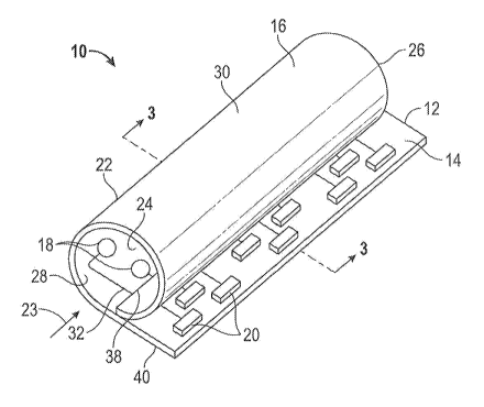
Referring now to the drawings, and more particularly to FIG. 1, shown
therein is an exemplary embodiment of a sensor assembly 10 constructed in
accordance with the inventive concepts disclosed and claimed herein. The
sensor
assembly 10 comprises a substrate 12 having a first surface 14 and a second
surface 16 opposite the first surface 14. At least one analyte sensor 18 is
positioned
on the first surface 14 of the substrate 12. At least one electrical contact
20 is
positioned on the substrate 12 in electrical communication with a
corresponding one
of the at least one analyte sensor 18. The substrate 12 is configured to
define a tube
22 defining a fluid flow path 23, and having a fluid inlet 24, a fluid outlet
26, an
interior surface 28, and an exterior surface 30. At least a portion of the
first surface
14 of the substrate 12 defines the interior surface 28 of the tube 22, and the
at least
one analyte sensor 18 is disposed on the interior surface 28 of the tube 22.
[0028] The
substrate 12 can be made from a number of materials such as
glass, plastic or a ceramic material such as an oxide of aluminum, silicon or
boron.
Suitable materials are well known to those skilled in the art. In one
embodiment, the
substrate 12 is a flexible material.
Nonlimiting examples of suitable flexible
6
CA 02871655 2014-10-21
WO 2013/163120 PCT/US2013/037695
materials include paper, polyethylene terephthalate (PET), polyethylene (PE),
polyimide (PI), polyether ether ketone (PEEK), and the like. Use of a flexible
substrate can reduce the size and weight of the sensor assembly 10. As
discussed
in detail in subsequent sections of this disclosure, use of a flexible
substrate can
allow increased circuit density and economic modification of the overall shape
of the
sensor assembly 10.
[0029] The
analyte sensor 18 positioned on the first surface 14 of the
substrate 12 can be any sensor capable of measuring a chemical or physical
parameter, such as the concentration of a chemical substance.
Nonlimiting
examples of sensor measurements in blood samples include pCO2, p02, pH, Na,
K+, Ca2+, Cl-, glucose, lactate, and hemoglobin. Many different types and
designs of
analyte sensors 18 can be used. Typically, the analyte sensor 18 includes two
or
three electrodes (not shown). The analyte sensor 18 may be in direct contact
with
the fluid being measured, and may include a thin membrane or the like
providing
indirect contact between the fluid and the electrodes in the analyte sensor
18. In one
embodiment, the analyte sensor 18 is an electrochemical biosensor and can
employ
conductivity, potentiometric, or amperometric techniques to convert the
chemical
information into a measurable signal.
[0030] For
example, biosensors based on conductivity techniques make use
of the fact that electrochemical reactions produce ions or electrons, and the
conductivity or resistivity of the solution changes proportionally.
Potentiometric
biosensors can utilize an ion-selective electrode or an electrode having an
ion-
permeable membrane that selectively permits the ion of interest to diffuse
through.
The operating principle is based on the fact that when a voltage is applied to
the
7
CA 02871655 2014-10-21
WO 2013/163120 PCT/US2013/037695
solution, there is a change in current flow due to electrochemical reactions.
Amperometric biosensors have high sensitivity for detecting electro-active
species
present in biological samples and are often used for analytes such as glucose
and
lactate. Amperometric biosensors utilize both working and reference
electrodes, the
working electrode being usually either a noble metal or a screen-printed layer
covered by a biorecognition component.
[0031]
Analyte sensors 18 can now be fabricated in a planar format, for
example by successively applying thin layers of materials to a base dielectric
substrate using thick-film and/or thin-film techniques. Planar analyte sensors
can be
made smaller and configured more closely together, reducing the sample volume
requirements. Manufacturing of planar thick-film electrodes on ceramic wafers
is
often done using standard processes. The use of ultrapure metals can be used
to
prolong use-life under constant polarization. Conductive and dielectric inks
have
been utilized, such as platinized carbon paste ink for screen-printing the
active
electrode of a glucose and lactate biosensor. Polymers can be used as an
internal
electrolyte such as Nafion, a sulfonated tetrafluoroethylene polymer, used as
an
internal electrolyte in some amperometric sensors for p02. For ion-selective
analyte
sensors, a copolymer of methacrylamidopropyltrimethylammonium chloride and
methyl methacrylate (MAPTAC/MMA) has been used as a solid internal contact.
[0032]
Thus, a wide variety of analyte sensors 18 can be used, alone or in
combination, with each analyte sensor 18 being in electrical connection with a
corresponding electrical contact 20 positioned on the substrate 12. In
one
embodiment, components of the analyte sensor 18, as well as the electrical
contact
20, utilize materials and methods recently developed and understood by those
8
CA 02871655 2014-10-21
WO 2013/163120 PCT/US2013/037695
skilled in the art, enabling circuits to be printed onto a flexible substrate
such as a
flexible polymer sheet. Such printed circuits are commonly referred to as flex
circuits. While known materials and methods of making flexible circuits are
described herein, it is understood that new and presently unknown materials
for
making and fixing the analyte sensor 18 and the electrical contact 20 onto a
flexible
substrate are also to be included in the presently disclosed and claimed
inventive
concepts.
[0033] Design and manufacture of the sensor assembly 10 with a flexible
substrate can include single-sided, double access, and double-sided flex
circuits.
Single-sided flex circuits have a single conductor layer made of either a
metal or
conductive (metal filled) polymer on a flexible dielectric film. Component
termination
features are accessible from one side. Holes may be formed in the base film to
allow
component leads to pass through for interconnection. Single sided flex
circuits can
be fabricated with or without such protective coatings as cover layers or
cover coats.
Double access flex circuits have a single conductor layer which is processed
so as to
allow access to selected features of the conductor pattern from both sides.
Double-
sided flex circuits actually have two conductor layers.
[0034] Polymer thick film flex circuits can be manufactured using
identical
components as used for rigid printed circuit boards, allowing the board to
conform to
a desired shape, or to flex during its use. Flex circuits are often made with
a
photolithographic technology. An alternative way of making flexible foil
circuits
includes laminating very thin copper strips in between two layers of PET.
These PET
layers are coated with an adhesive which is thermosetting, and will be
activated
during the lamination process.
9
CA 02871655 2014-10-21
WO 2013/163120 PCT/US2013/037695
[0035] In one embodiment, conductive inks and dielectric inks are
deposited
onto the substrate 12 using screen printing, rotogravure, pad printing,
stenciling,
jetting and the like to provide the electrical contact 20, as well as
electrodes and
other components of the analyte sensor 18. The conductive ink may be formed in
part by nanoparticle platinum, gold, silver, copper, silicon, or any other
conductive
element or combination of elements. Membrane materials are applied to
appropriate
areas of the substrate 12 to produce a functioning analyte sensor 18. The
substrate
12 is flexible and can be made from paper, polyethylene terephthalate (PET),
polyethylene (PE), polyimide (PI), and the like.
[0036] The electrical contact 20 in electrical communication with the
corresponding analyte sensor 18 can be any shape and any conductive material.
Suitable materials for the electrical contact 20 include, but are not limited
to, gold,
silver, copper and aluminum metals and alloys thereof as well as conductive
inks.
[0037] In one embodiment, the electrical contact(s) 20 is positioned on
the first
surface 14 of the substrate 12, as exemplified in FIG. 1 through FIG. 3.
Electrical
communication between the analyte sensor 18 and the electrical contact 20 can
be
achieved using a trace 32, also positioned along the first surface 14 of the
substrate
12. The trace 32 can be a strip of conductive metal such as copper, conductive
ink,
and the like, capable of making an electrical connection to carry signals
between the
analyte sensor 18 and the electrical contact 20. The electrical contact 20 is
positioned, sized and shaped to mesh with an electrical contact to an analyzer
(not
shown) for processing and outputting analyte results based on analyte sensor
measurements of a fluid sample.
CA 02871655 2014-10-21
WO 2013/163120 PCT/US2013/037695
[0038] In another embodiment, the electrical contact(s) 20 is positioned
on the
second surface 16 of the substrate 12, as exemplified in FIG. 4 through FIG.
6.
Electrical communication between the analyte sensor 18 positioned on the first
surface 14, and the electrical contact 20 positioned on the second surface 16,
can be
achieved using a trace 32 which can be partly positioned along the first
surface 14 of
the substrate 12. The trace 32 passes through a hole or via 34 at some point
to
connect to the corresponding electrical contact 20 on the second surface 16.
The
via 34 can be, for example, a bore filled with an electrical conductive
material, e.g., a
metal or conductive ink.
[0039] The substrate 12 can be configured to define the tube 22 by, for
example, rolling, bending or folding the substrate 12 to the desired shape. In
one
embodiment, the substrate 12, to which has been attached the analyte sensor,
electrical contact 20, trace 32, and other necessary or desired electrical
components
and connections (referred to collectively as "circuit 36") can be planar
during
application of the circuit 36, and then rolled to form a tube 22 having a
circular cross-
section as in FIG. 1 through FIG. 6. In another embodiment, the substrate 12
with
attached circuit 36 can be bent or folded to form a tube 22 having at least
three
planar sides as, for example, in FIG. 7 and FIG. 8.
[0040] The tube 22 has a fluid inlet 24 and a fluid outlet 26, as well as
an
interior surface 28 and an exterior surface 30. The sensor assembly 10 can be
constructed on a unitary one piece substrate 12, the sensor assembly 10 having
only
a single seam 38 that can be secured using pressure sensitive adhesive, epoxy,
acrylic, or other bonding means and materials known to those skilled in the
art. The
need for a spacer material is eliminated. Additionally, multiple analyte
sensors 18
11
CA 02871655 2014-10-21
WO 2013/163120 PCT/US2013/037695
can be printed onto a film, for example, with sufficient distance between
electrodes
to minimize cross-talk and other interference. When the substrate 12 and
analyte
sensors 18 are rolled into a tube configuration, sensor placement becomes both
opposing and adjacent, thereby enabling a higher number of analyte sensors 18
in a
smaller fluidic path.
[0041] In one embodiment, the electrical contact(s) 20 is positioned on
the
second surface 16 of the substrate 12 as exemplified in FIG. 4 to FIG. 6. The
electrical contact(s) 20 can be readily connected to the analyzer using, for
example,
a receiving portal with an electrical contact(s) configured to mesh with the
electrical
contact(s) 20 on the outer surface of the tube 22.
[0042] In one embodiment, the electrical contact(s) 20 is positioned on
the first
surface 14 of the substrate 12, as exemplified in FIG. 1 through FIG. 3, FIG.
7 and
FIG. 8, and the substrate 12 is rolled, bent or folded to leave a tab 40
extending from
the tube 22 and having the electrical contact 20 positioned on the tab 40. The
tab 40
can extend in a tangential relationship to the tube 22. The tab 40 can be
readily
connected to the analyzer using, for example, a ribbon-type connector
configured to
mesh with the electrical contact(s) 20 and the tab(s) 40 to transfer
electrical signals
for processing and outputting analyte results based on sensor measurements of
a
fluid sample.
[0043] Referring to FIG. 2, an amplifier front-end circuit 42 can be
positioned
on the first surface of the substrate proximate to and in electrical
communication with
a corresponding one of the at least one analyte sensor 18. The amplifier front-
end
circuit 42 can be useful when the analyte sensor 18 produces a low-range
output
susceptible to interference and noise. Such interference and noise can corrupt
the
12
CA 02871655 2014-10-21
WO 2013/163120 PCT/US2013/037695
integrity of a signal transferred along the trace 32. The amplifier front-end
circuit 42
amplifies the signal from the analyte sensor 18 before communicating the
signal to
the analyzer (not shown) for processing and outputting analyte results. The
amplification reduces signal loss and improves the risk of corrupting the
signal
integrity while it is communicated to the analyzer.
[0044] As
with the analyte sensor 18, the amplifier front-end circuit 42 may be
formed by printing, using a conductive ink, directly on the substrate 12, or
onto a thin
film membrane later applied to the substrate 12. The amplifier front-end
circuit 42 is
positioned on the substrate 12 in close proximity to the analyte sensor 18 and
electrically connected along the trace 32.
[0045]
Referring now to FIG. 9, the sensor assembly 10 can include a first cap
43 covering the fluid inlet 24 and/or a second cap 43' covering the fluid
outlet 26.
The first cap 43 may include a nipple 44 for facilitating insertion of the
fluid sample to
be analyzed into the tube 22. Similarly, the second cap 43' may include a
nipple 44'
to facilitate removal of the fluid sample from the tube 22.
[0046] In
one embodiment, the sensor assembly 10 includes a collar 45 and
optionally a collar cap 46 as shown in FIG. 10. The collar 45 facilitates
manual
insertion of a liquid sample into the sensor assembly 10 and is easy to handle
and
store. The collar 45 also facilitates moving the sensor assembly to and from
the
analyzer.
[0047]
Referring now to FIG. 11, shown therein is another exemplary
embodiment of a sensor assembly 10 constructed in accordance with the
inventive
concepts disclosed and claimed herein. In this embodiment, the substrate 12 is
configured to define a tube 22 having an interior surface 28', and an exterior
surface
13
CA 02871655 2014-10-21
WO 2013/163120 PCT/US2013/037695
30'. At least one analyte sensor 18 is disposed on the exterior surface 30' of
the
tube 22, while the corresponding electrical contact 20 is positioned on the
interior
surface 30' of the tube 22. It is contemplated that a sensor assembly 10 with
this
arrangement could be used as a cannula for inserting into the body for making
fluid
measurements. Wiring 50 can be housed within the tube 22, and body fluid can
be
accessed on the exterior surface 30' of the tube.
[0048] The embodiment shown in FIG. 11 can also be housed within an outer
cannula 52, as shown in FIG. 12, with the tube 22 and the outer cannula 52
defining
an annulus 54 therebetween. Blood or other fluid to be monitored flows through
the
annulus 54 and is measured by the one or more analyte sensor(s) 18. A cap 43'
prevents fluid from entering the interior of the tube 22. When used for
insertion into
a patient's body, the outer cannula 52 is made of material harmless to the
human
body. This design can be useful in situations where a patient's exposure, or
prolonged exposure, to the exterior surface 30' of the tube 22 is
undesireable.
[0049] A method of forming a sensor assembly includes the step of forming
a
plurality of analyte sensors on a surface of a flexible substrate, as
described above.
A plurality of electrical contacts are formed on the flexible substrate such
that the
electrical contacts are in electrical communication with a corresponding one
of the
analyte sensors. The flexible substrate is then configured to define a tube
having a
fluid inlet, a fluid outlet, an interior surface, and an exterior surface with
the surface
on which the analyte sensors are formed defining the interior surface of the
tube
such that the analyte sensors are disposed on the interior surface of the
tube. If
desired, the sensor assembly can be treated chemically or by heat to add
rigidity.
14
CA 02871655 2014-10-21
WO 2013/163120 PCT/US2013/037695
Optionally, a stiffener can be attached to the sensor assembly to support and
maintain the overall shape.
[0050] Similarly, another method of forming a sensor assembly includes
the
steps of forming a plurality of analyte sensors on a surface of a flexible
substrate,
and forming a plurality of electrical contacts on the flexible substrate such
that the
electrical contacts are in electrical communication with a corresponding one
of the
analyte sensors. In this case, the flexible substrate is configured to define
a tube
having an interior surface and an exterior surface with the surface on which
the
analyte sensors are formed defining the exterior surface of the tube such that
the
analyte sensors are disposed on the exterior surface of the tube.
[0051] From the above description, it is clear that the inventive
concept(s)
disclosed herein is well adapted to carry out the objects and to attain the
advantages
mentioned herein as well as those inherent in the inventive concept disclosed
herein.
While exemplary embodiments of the inventive concept disclosed herein have
been
described for purposes of this disclosure, it will be understood that numerous
changes may be made which will readily suggest themselves to those skilled in
the
art and which are accomplished without departing from the scope of the
inventive
concept disclosed herein and defined by the appended claims.