Note: Descriptions are shown in the official language in which they were submitted.
CA 02871822 2014-10-28
WO 2013/175326
PCT/1B2013/053382
1
SPIN LOGIC BASED ON PERSISTENT SPIN HELICES
FIELD OF THE INVENTION
The invention relates in general to the fields of spin logic devices
implementing logic circuits,
in particular majority logic circuits.
BACKGROUND OF THE INVENTION
A number of concepts have been proposed that are based on the electron spin,
like cellular
automata. In particular, spin devices have been suggested, which include a
spin transport
layer (or STL) above a substrate. Connected to the STL are input and output
electrodes. The
input electrodes act as spin injection contacts and consist of a magnetic
material that is
magnetized into one of two possible directions (spin up/down). By passing a
current between
the input electrodes and the STL, spin-polarized electrons can be accumulated
in the STL at
the interface between the input electrode and the STL. The spin polarization
of electrons at
that location in the STL is directly related to the magnetization of the input
electrode, i.e. the
spins in the STL are also either up or down. The output electrodes convert the
local spin
polarization at the interface between the STL and the output electrode. Spin
polarization is
e.g. converted into an electrical signal. The concepts of input and output
electrodes acting as
spin injection and spin detection contacts are well described in literature.
Also the concept of
spin amplification where the magnetization of a detection electrode takes over
the spin
polarization in a STL is known. In between the input and output electrodes,
the spin
polarization imprinted by the input electrode propagates by diffusion or
drift.
Besides, it has been demonstrated how logic gates can be constructed using
majority-logic
concepts where several input electrodes polarize the electron spin in the STL
and the output
electrode detects the average spin polarization that diffuses from those input
electrodes to the
output electrode.
BRIEF SUMMARY OF THE INVENTION
According to a first aspect, the present invention is embodied as a spin logic
device,
comprising:
an electron confinement layer confining an electron gas or 2DEG in a two-
dimensional area
subtended by a direction x and a direction y, the latter perpendicular to the
former, the spin
logic device configured for the 2DEG to support a persistent spin helix or PSH
formed
CA 02871822 2014-10-28
WO 2013/175326
PCT/1B2013/053382
2
therein with a given spin component oscillating with periodicity k along
direction x but not
oscillating along direction y; and
a logic circuit, said circuit comprising: one or more input devices,
energizable to create
respective local spin-polarizations of the 2DEG in respective first regions of
the confinement
layer, such as to form respective PSHs; and an output device, configured to
detect, in a
second region of the confinement layer, an average spin-polarization of the
2DEG resulting
from one or more local spin-polarizations created by the one or more input
devices and
diffused through one or more resulting PSHs, respectively,
wherein a projection of a distance between the second region and any one of
the first regions
onto said direction x is equal to n Va, n integer, a equal to 2 or 4.
In embodiments, the logic circuit is a majority logic circuit that comprises
three or more input
devices, said three or more input devices preferably including three input
devices aligned
along direction y.
In particular, the majority logic circuit may comprise at least two logic
inputs and one control
input.
Preferably, the output device is configured to detect an average spin-
polarization for: said
given spin component if a = 2; and/or a perpendicular spin component if a =4
and n is odd.
According to embodiments, the spin logic device further comprises an
additional set of one or
more input devices, energizable to create respective local spin-polarizations
of the 2DEG in
respective third regions of the confinement layer, such as to form respective
PSHs, wherein a
projection of a distance between any one of the third regions and any one of
the first regions
onto said direction x is equal to 1 Va, 1 integer, a equal to 2 or 4, with
preferably 1= n.
Preferably, said output device is a first output device and the spin logic
device further
comprises an additional output device, opposite to the first output device
with respect to the
one or more input devices, the additional output device configured to detect a
spin-
polarization of the 2DEG within a fourth region of the confinement layer, the
fourth region at
a distance from the first region, a projection of said distance onto direction
x being equal to m
Va., m integer, a equal to 2 or 4, and wherein preferably m = n.
In preferred embodiments, the spin logic device further comprises at least one
output device
configured with respect to one or more input devices to detect an average spin-
polarization of
the 2DEG propagating along direction y in the confinement layer.
CA 02871822 2014-10-28
WO 2013/175326
PCT/1B2013/053382
3
In embodiments, the spin logic device comprises three or more layers of
semiconductor
materials, the electron confinement layer formed within one of said three or
more layers or at
an interface between two contiguous layers of said three or more layers.
Typically, the layers of semiconductor materials determine a symmetry of the
spin-orbit
interaction or SOT to which the 2DEG is exposed such that the 2DEG is adapted
to support
said PSH.
For instance, the layers of semiconductor materials define a given bulk
inversion asymmetry
and a given structure inversion asymmetry, the symmetry of the SOT determined
by said
given bulk inversion asymmetry and said given structure inversion asymmetry.
The input devices may be electrodes, whose extension dimensions along
direction x is less
than k/2, and preferably less than k/4.
Preferably, a distance between the second region and the closest one of the
first regions is
equal to n Va., n integer, a equal to 2 or 4, and wherein, preferably, a = 2
and n = 4.
According to another aspect, the invention is embodied as a method of
operating a spin logic
device according to any one of the above embodiments, the method comprising:
energizing one or more of the input devices ; and
detecting an average spin-polarization of the 2DEG via the output device.
In preferred embodiments, the logic circuit of the spin logic device is a
majority logic circuit
that comprises at least two logic inputs and at least one control input, and
energizing
comprises energizing each of the two logic inputs and the control input to
create respective
local spin-polarizations of the 2DEG.
Preferably, the created spin-polarizations exhibit opposite spin-
polarizations.
Devices and methods embodying the present invention will now be described, by
way of non-
limiting examples, and in reference to the accompanying drawings.
BRIEF DESCRIPTION OF SEVERAL VIEWS OF THE DRAWINGS
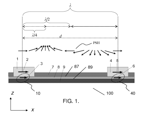
- FIG. 1 is a section view of a simplified representation of a spin-logic
device, according to
embodiments;
CA 02871822 2014-10-28
WO 2013/175326
PCT/1B2013/053382
4
- FIGS. 2.A - C represent density plots (direct mapping, simulated), where
representative
contours have been emphasized, illustrating the formation of a persistent spin
helix at three
different times after spin injection;
- FIGS. 3 ¨ 8 schematically illustrate the construction of logic gates using a
persistent spin
helix to propagate information from spin injection devices to output devices,
according to
embodiments. In particular:
- FIGS. 3.A - B represent density plots (direct mapping, simulated),
illustrating persistent
spin helices formed upon parallel spin injections. Depictions of components of
a majority
logic circuit are superimposed to the density plots. Spin injection and
detection correspond to
OR logic gate operations in regard to inputs A and B.
- FIGS. 3.0 ¨ 3.D are simplified representations for FIGS. 3.A ¨ B;
- FIGS. 4.A - B schematically illustrate AND logic gate operations;
- FIG. 5 illustrates an inversion (NOT) operation;
- FIG. 6 is an example of combined logic gate calculating (A OR B) AND D;
- FIG. 7 illustrates the construction of two logic gates (A OR B) and (A
AND B);
- FIG. 8 is an example of OR gate along a direction where the spin does not
oscillate, as
additionally involved in embodiments; and
- FIG. 9 shows details of a majority logic circuit as involved in
embodiments.
DETAILED DESCRIPTION OF THE INVENTION
The following description is structured as follows. First, general embodiments
and high-level
variants are described (sect. 1). Technical implementation details are
discussed in the second
section.
1. General embodiments and high-level variants
In reference to FIG. 1, an aspect of the invention is first described, which
concerns a spin
logic device 100. FIG. 1 is a side view of a simplified representation of such
a spin-logic
CA 02871822 2014-10-28
WO 2013/175326
PCT/1B2013/053382
device, according to embodiments. Briefly, this view represents components of
the device,
including various layers of semiconductor materials 7, 8, 9, as well as a spin
injection (input)
device 1 and a spin detection (output) device 4. The device 100 is configured
to enable the
formation of persistent spin helices (or PSHs) having periodicity k along
direction x, as
5 symbolically represented above the device 100.
In more detail, the device 100 first comprises an electron confinement layer,
the latter
confining an electron gas in a two-dimensional area (this electron gas is
accordingly later
referred to as 2DEG, for simplicity). The two-dimensional area is subtended by
perpendicular
directions x and y (direction y is perpendicular to the plane of the drawing).
Typically, the
device 100 comprises three or more layers 7, 8, 9 of semiconductor materials:
the electron
confinement layer is for example formed within layer 8, or at an interface 87
or 89 between
two contiguous layers 7, 8 or 9. Additional layers may be involved. The layers
7, 8, 9 may
themselves decompose into sub-layers, as needed, to achieve a 2DEG with
suitable properties.
However, the 2DEG may be confined within only one layer of semiconductor
material. In
variants, the electron confinement layer may be formed at an interface between
a layer of
semiconductor material and an additional layer of a semiconducting, metallic
or insulating
material.
How to achieve this shall be discussed later in details. For the time being,
we assume that the
device 100, and in particular the layers 7, 8, 9 of semiconductor materials
can be engineered
such that the 2DEG can support a helical spin mode. More precisely, a PSH
formed in the
2DEG shall have a given spin component, e.g., S, or Sx, oscillating with
periodicity k along a
given in-plane direction, for example direction x, but not oscillating along
the perpendicular
(in-plane) direction y.
Second, the device 100 comprises a logic circuit, which preferably is
configured as a majority
logic circuit. Said circuit includes one or more input devices 1 (only one
such device appears
on FIG. 1.), i.e., spin-injection devices, which upon suitable energization
create local spin-
polarizations 3 of the 2DEG in respective first regions 10 of the confinement
layer. Said "first
regions" 10 are also referred to as "input regions" or "spin injection
regions" in the following.
If the input devices are simple electrodes, as in the example of FIG. 1, the
first regions 10
simply correspond to locations (in x) of the electrodes. Other types of input
devices and spin
injection mechanisms shall be discussed later.
Specific designs of electron confinement layers as assumed herein are such
that a local spin
excitation shall evolve into a PSH. Thus, local spin-polarizations 3 shall
result in the
CA 02871822 2014-10-28
WO 2013/175326
PCT/1B2013/053382
6
formation of respective PSHs, through which spin-polarizations "helically"
propagate,
resulting in spin oscillations, as schematically depicted in FIG. 1 too. Thus,
the PSH-based
spin propagation involves oscillations, beyond mere spin diffusion.
A spin-detection device 4, or simply "output device" is furthermore provided
to detect, in a
second region 40 of the confinement layer, an average spin-polarization 6 of
the 2DEG that
results from the spin-polarizations propagated through the PSHs. The "second
region" 40
may also be hereafter referred to as the "output region" or "detection
region".
As it can further be realized from FIG. 1, to properly exploit the spin-
polarization information
as diffused along PSHs, the distance d between a region 10 of spin-injection
and a detection
region 40 must be set according to the oscillation periodicity X along
direction x. For example,
in FIG. 1, the detection region 40 is at a distance d = X from the region 10
of spin-injection.
However, it may further be realized that the detection region 40 could be set
at a distance d =
k/2 from the first region 10. At d = k/2, the polarization is simply reversed
with respect to d =
X. Furthermore, detection can even be set at d = k/4, provided that the output
device is able to
detect perpendicular spin-polarizations. Note that in FIG. 1 the distance
between input/output
regions corresponds to the distance between input/output devices since the
latter are assumed
to be electrodes in that case, which electrodes enable spin
injection/detection at their
respective positions along x. However, this need not be always the case,
depending on the
spin injection/detection mechanism chosen. Thus, it is the distance d between
input/output
regions that must be set according to k, rather than the distance between
input/output devices.
So far, the distance d referred to above corresponds to direction x in FIG. 1,
as the latter is a
section view. Now, location constraints as to the other direction y
(perpendicular to the
section view of FIG. 1) are much less stringent, since spin polarization
diffuses along y and
does not oscillate. This point is now discussed in reference to FIGS. 2.A ¨ C,
which show
density plots, representing a PSH formation (direct mapping), as obtained from
simulations.
The latter were obtained thanks to a custom-made program, using a Monte-Carlo
approach,
which takes into account spin diffusion and precession of spin about the spin-
orbit field;
typical material parameters for a GaAs/AlGaAs quantum well structure were
used.
Representative contours have been emphasized in the density plots. At variance
with FIG. 1,
initial spin polarization is along z-axis in this example. The density plots
capture the
formation of a PSH at three different times after spin injection, namely 25,
300, and 900 ps, it
being noted that the lifetime of a PSH is on the order of nanoseconds. It is
noted, in that
respect, that detection can be optimally synchronized with injection. The
maximal amplitudes
at a distance d from the input region will be reached a certain time after
injection that
depends on the spin diffusion constant D and is given by d2/D (typically 1 ns
for d = 5 1..tm for
CA 02871822 2014-10-28
WO 2013/175326
PCT/1B2013/053382
7
GaAs quantum wells). Timing can thus be adjusted by varying distance d between
input/output regions and/or selecting materials having suitable parameters.
As seen in FIGS. 2.A ¨ C, owing to the quite "large" diffusion observed along
y, there is no
need to set detection at y = 0, i.e., vis-a-vis the injection region.
Formally, what is needed is
that the projection onto axis x of the distance d between the second region 40
and the first
region 1 (or more generally any one of the injection regions) be "in-phase"
with characteristic
polarizations of the PSH. In mathematical terms, this projection, call it dx,
should be
essentially equal to n V a, with n integer and a equal to 2 or 4. Thus, one
may typically have
dx equal to k/4, k/2, or k, etc.
This opens the possibility to use several input devices 1. In this regard, the
logic circuit is
preferably configured as a majority logic circuit, which typically comprise
three or more
input devices. Preferably, an odd number of inputs are used, to enable
"majority". This is
however not always the case, as exemplified in FIG. 7. In the simplest
implementations, these
input devices (or subsets thereof) are typically aligned parallel to direction
y, as to be
discussed later in detail in reference to FIGS. 3 ¨ 8. Of course, this shall
not be the case if
input devices are purposely shifted (as in FIG. 7), e.g., for inverting the
input state.
As illustrated in FIGS. 3 ¨ 4, detection is nonetheless preferably set vis-a-
vis the input
devices. Formally, this means that the distance between the second region 4
and the closest
one of the first regions 1 (corresponding e.g., to the input device in the
middle) is preferably
set equal to n V a, with n integer, and a equal to 2 or 4 (a = 2 and n = 4 in
the examples of
FIGS. 3 ¨ 4). In other words, detection can be set in front of one of the
inputs. Similarly, if
the detection region is chosen to extend over a large distance, e.g.,
comparable to the length
of extension of the input devices along y, then the output device is
preferably located vis-a-
vis the input devices.
Ideally, the injection/detection regions should be located as accurately as
possible, to exploit
maximal amplitudes of the spin-polarization. However, it can be realized from
FIG. 1 or 2
that slight misalignments are not critical. A misalignment is tolerated as
long as it can clearly
be discriminated amongst two spin polarizations of interest, which otherwise
depend on the
distance retained. The misalignment should not exceed k/4, as it can be
realized from FIG. 1.
Yet, much larger signal magnitudes are obtained in practice if the
misalignment is smaller
than k/8. Thus, one understands that the projection dx of distance d onto axis
x should be
essentially equal to n V a, i.e., equal to n kla klb with b > 4 (preferably
b> 8). Accordingly,
if the input/output devices used are electrodes, the extension dimensions of
the latter along x
CA 02871822 2014-10-28
WO 2013/175326
PCT/1B2013/053382
8
should typically be less than k/2 (assuming perfect alignment), and preferably
less than k/4 (if
the misalignment remains smaller than k/4).
Next, input/output devices can be of any suitable type; such devices are known
per se.
However, more versatile spin logic devices shall be obtained if each spin
injection device is
able to selectably inject spins up and spin down. Suitable spin injection may
notably occur
through spin transfer from a ferromagnetic layer into the confinement layer,
by means of
photoexcitation, or by any spin-dependent transport process, as e.g. spin-
dependent tunneling.
Similarly, various spin-polarization detection methods are known. For example,
the created
and detected spin polarization is along a given direction that is
perpendicular to the spin-orbit
magnetic field. The direction of the spin-orbit magnetic field depends on the
crystalline
direction along which the electron confinement is realized, e.g. in zincblende
semiconductors
supporting a persistent spin helix, this direction is in-plane (along y) for
confinement along
[100], and out-of-plane for confinement along [110]. Therefore, two possible
directions for
created and detected spin polarization are along x and out-of-plane for [100]
confinement,
and along x and along y for [110] confinement.
Thus, the present invention can be embodied with output devices 4 configured
to detect an
average spin-polarization for any spin component that oscillates along x, for
example
components S, or Sx in FIG. 1. Notably, if dx = n Vet with a = 4 and n odd,
then the output
device should be configured to detect spin polarization that is along a
direction perpendicular
to the direction of spin polarization injected by the input device. For
example, the output
device could be configured to detect perpendicular spin-polarization rather
than in-plane.
More generally, use can be made of spin-polarization input/output devices that
create/detect
in-plane and/or out-of plane spin polarizations.
Next, FIGS. 3.A ¨ B represent simulated density plots of PSHs, which are
formed (step S30)
after spin-injections (step S20) at input devices la, lb and lc. Spin-
injection is ideally carried
out simultaneously at the input devices, i.e., such as to create parallel PSHs
that progressively
merge. The input devices 1a, lb and 1c, together with the output device 4, are
schematically
represented as superimpositions to the density plots. In FIG. 3.A, the initial
spin polarizations
(along x in this example) are the same at each input device, and assumed to
correspond to
spin up or logical value "1". The initial, parallel polarizations evolve into
respective PSHs,
which partly overlap and merge such as to lead to a stripe pattern similar to
that of FIG. 2.B
or C. Note that in FIG. 3.B, the initial spin polarizations at input devices
la, lc are the same,
but are opposite to initial polarization at device lb. The latter is assumed
to correspond to
spin down or logical value "0", as shown in the legend. In that case, a mixing
of spin
polarization in the STL results, which reflects how spin propagation is
modulated in that case.
CA 02871822 2014-10-28
WO 2013/175326
PCT/1B2013/053382
9
This mixing notably affects the average polarization that results in the
region corresponding
to the output device 4.
In each of FIG. 3.A or B, the initial polarizations are synchronously
inputted, at the level of
first regions corresponding to the input devices la ¨ c. The output device 4
subsequently
detects (step S40) the average spin-polarization that results at the level of
the detection region.
Detection can be timely set, e.g., 1 ns after injection. As illustrated in
FIG. 3.A, the PSHs that
are fully in phase in that case result in a "large" average spin-polarization
(along x) at the
level of the detection 4. If, on the contrary, the created spin-polarizations
exhibit opposite
spin-polarizations as in FIG. 3.B, the PSHs are only partly in phase,
resulting in a "lower"
average spin-polarization at the output 4. More schematical depictions of
FIGS. 3.A ¨ B are
given in FIGS. 3.0 ¨ D. Beyond these two examples, several combinations of
spin-
polarization can be contemplated for the injection, a thing that enables
implementation of
majority logic together with PSHs, using one of the inputs, e.g., input lc, as
a control input.
More precisely, devices such as described above allow for intermingling
majority logic
concepts with PSHs. In particular, an advantage of PSHs is that one can easily
reverse the
injected/detected values. For example, one can reverse the output by shifting
the output
device by m k/2, m odd, along x. This has fantastic advantages for the
construction of logic
devices. In this regard, using dx = n V a with small values of n and/or with a
= 4 reduces the
footprint of the logic arrays, thereby enabling high integration density. On
the other hand,
using dx = n V a with large values of n allows for building more complex logic
arrays, notably
by adding more input/output devices at definite locations on the PSH.
These points are now discussed in more detail in reference to FIGS. 3C ¨ 8,
which
schematically illustrate the construction of logic gates using a PSHs to
propagate information
from spin injection devices 1, la, lb, etc. to output devices 4, 4a, 4', etc.,
according to
various embodiments. Basically, in each of the embodiments of FIGS. 3.0 to 8:
the spin logic
devices 100 are operated as follows:
- First, one or more of the input devices are energized, step S20, to create
local spin
polarizations in correspondence with the input devices. Owing to the specific
device
conceptions as contemplated here, one or more PSHs correspondingly develop,
step S30; and
- Second, an average spin-polarization is detected via the output device(s),
step S40.
Some applications (e.g., FIGS. 3, 4, 6 and 7) make advantageously use of
majority logic
where two or more logic inputs (e.g., A and B in FIGS. 3 ¨ 4) and one control
input C, each
provided by respective input electrodes la, lb and lc, are wired together, and
the result of the
CA 02871822 2014-10-28
WO 2013/175326
PCT/1B2013/053382
logic gate is determined by the average of spin-polarization resulting from
the three inputs at
the level of the output electrode 4.
In FIGS. 3 to 7, the view is "onto" the 2DEG (plane (x, y)) with the direction
of the PSH
5 oscillation along the horizontal x direction. The direction in which spin
polarization stays
constant is along the y direction. Spin polarization is encoded in a grey
scale. Black means
spin up and white spin down. As touched earlier, spin up and down are defined
as spin
polarization along or against a specific direction that can be either the
direction perpendicular
to the 2DEG or the direction along which the PSH forms (x-axis in the
drawings). Spin
10 signals propagate along x (they also diffuse along y, yet without
oscillating).
Briefly, AND and OR logic gate operations can be performed by propagating spin
along
either the x or the y direction, whereas inversion (NOT) is implemented by
spin propagation
along the x direction. Examples of AND, OR and NOT gates realized using spin
propagation
along the x direction are shown in FIGS. 3 ¨ 5. A cascade of two logic gates
using spin
propagation along both x and y directions is shown in FIG. 6. Since spin
propagates along all
directions, one input electrode can provide input spin polarization for
several gates where
propagation of spin polarization is along different directions. FIG. 7 shows
an example where
two different logic gates (A AND B) and (A OR B) are realized using spin
propagation along
+x and ¨x directions. This construction uses two input electrodes 1 providing
inputs A and B.
The two logic gates use spin that propagates along ¨x (A OR B) or +x (A AND B)
direction.
Finally, an example of an OR gate with spin propagation along the y direction
is shown in
FIG. 8. In this latter case however, no use is made of the PSH mode, such that
no simple
reversal is possible in that case.
In FIGS. 3.0 ¨ D, 4.A ¨ B, and 6 ¨ 8, the logic circuit is designed as a
majority logic circuit.
Referring more particularly to FIGS. 3 ¨ 4, the circuit may for instance
comprise three (or
more) input devices la, lb, lc, aligned along direction y. This includes two
logic inputs la,
lb and one control input lc (at least). Of course, simpler logic gates such as
NOT shall need
only one input and one output, as illustrated in FIG. 5, and therefore do not
require a majority
logic. In the latter case, one can clearly understand the interest of a PSH,
which allows for
simple inversion, over a distance of X/2. Yet, the minimum feature size is
generally not
limited to X12, as already touched upon above.
More complex gates can be designed, as exemplified in FIGS. 6 ¨ 7. FIG. 6 is
an example of
a combined logic gate calculating (A OR B) AND D. In this regard, the spin
logic device 100
may further comprise an additional set of input devices 1c2, ld, functionally
similar to those
described earlier. This additional set allows for injection at a distance from
both the input
CA 02871822 2014-10-28
WO 2013/175326
PCT/1B2013/053382
11
regions corresponding to the first set of input devices la, lb, 1c1 and the
output regions
corresponding to output device 4. Again, references la, lb refer to logic
inputs while 1c1 and
1c2 refer to control inputs. In the following, the injection (resp. detection)
regions are
assumed to correspond to the x-locations of the corresponding input (resp.
output) devices,
for simplicity (as this is the case with electrodes). Formally, the x-
projection of the distance
between any one of the additional injection regions 1c2, id and any one of the
first injection
regions la, lb, 1c1 is equal to 1 Va., where 1 is integer and a is equal to 2
or 4. One may for
instance have 1 = n/2 = 2, like in the example of FIG. 6.
FIG. 7 illustrates the construction of two logic gates, (A OR B) and (A AND
B). In this
regard, the spin logic device 100 may further comprise an additional output
device 4a,
opposite to the first output device 4 with respect to input devices 1a, lb,
the additional output
device configured to detect an average spin-polarization within a respective
region (call it
"fourth" region) of the confinement layer. The fourth region 4a is at a
distance from the first
region 1, a projection of said distance onto direction x being equal to m Va,
m integer, a equal
to 2 or 4, and wherein preferably m = n (it being reminded that the second
detection region 4
is located at n Va from the first region 1). Note that the control inputs are
shifted with respect
to the logic inputs in the example of FIG. 7.
For completeness, although embodiments above all take advantage of a PSH, it
does however
not prevent a device 100 to comprise additional components, to enable logic
gates in
directions where no-spin oscillation arises, e.g., direction y in the appended
drawings. For
example, the spin logic device 100 may further comprise an output device 4'
configured with
respect to input devices la', lb', lc' (aligned along x) to detect an average
spin-polarization
propagating along direction y, as illustrated in FIG. 8. FIG. 8 is an example
of an OR gate
along direction y, where the spin does not oscillate.
Finally, in each of the embodiments of FIGS. 3 ¨ 6 and 8, only one detector 4
is shown,
which measures an average spin-polarization in a corresponding, finite
detection region. This
detector is typically located in front of a control electrode, which itself is
located in the
middle of an aligned set of input electrodes; this gives some symmetry with
respect to the two
input states, but is not necessary. Rather, the control input electrode may be
at any position
along y (or at least close enough to the logic inputs to enable the
correspondingly formed
PSHs to merge) , and the output electrode is preferably set symmetrically to
the position of
the three input electrodes, i.e. at the y position of the middle input
electrode. In variants, a set
of several detectors 4 could be used, aligned such that each detector faces an
input electrode.
An average of the spin-polarizations as measured via each of the output
electrodes could
accordingly be performed, to enable majority logic. Such variants require more
complex
CA 02871822 2014-10-28
WO 2013/175326
PCT/1B2013/053382
12
circuits. On the other hand, they may allow for clearer discrimination between
spin-
polarizations.
2. Technical implementation details
This section describes in more detail:
- how to use a 2DEG as a STL;
- how said 2DEG has to be designed in order to allow for propagation of
spins over
large distances; and
- how the STL has to be designed in order for the spin polarization in the
2DEG to
spatially alternate between spin up and spin down, forming a PSH.
In reference to FIG. 1, the STL may be obtained by way of semiconductor layers
7, 8, and 9
hosting the 2DEG. The 2DEG can for example be confined to a quantum well, i.e.
to
semiconductor layer 8 in FIG. 1, where electrons are in states of lower energy
than in the
surrounding layers 7 and 9. In variants, the 2DEG can be located at an
interface, i.e., between
layer 8 and either layer 7 or 9. The electrons in that 2DEG typically provided
by dopants in
layers 7, 8 and / or 9. The material of such semiconductor layers can be
alloys and ternary
alloys of III-V materials (e.g. GaAs, AlAs, InAs, InP, InSb) or II-VI
materials (e.g. CdSe,
CdTe, ZnSe).
In variants, the 2DEG may be formed within a single semiconductor layer, at
the interface
with a contiguous insulating or metallic layer, and electrons are provided by
field-effect using
an electric field. In addition, an electric field applied perpendicular to the
layer may be used
to condition the system for it to be able to support a PSH, if necessary.
Connected to the 2DEG are input 1 and output 4 electrodes, as evoked earlier.
The input
electrodes act as spin injection contacts and consist of a magnetic material
that is magnetized
into one of two directions, i.e., spin up or spin down, as denoted by
reference 2 in FIG. 1. In
the example of FIG. 1, the injection direction is along direction x. By
passing a current
between the input electrodes and the 2DEG, spin-polarized electrons can be
accumulated in
the 2DEG in a given injection region 10, e.g. at the interface between the
input electrode and
the 2DEG. The spin polarization of the electrons at that location in the 2DEG
is directly
related to the magnetization of the input electrode, i.e. the spins in the
2DEG are also either
up or down. The output electrodes convert the local spin polarization in the
output region
(typically at the interface between the 2DEG and the output electrode) into
either an electrical
signal or into a magnetization state of another input electrode: the latter
can be said output
electrode or another electrode close-by that takes over the spin polarization
of the 2DEG at
CA 02871822 2014-10-28
WO 2013/175326
PCT/1B2013/053382
13
the interface. This makes it possible to amplify the spin polarization of the
2DEG into a
magnetization of the ferromagnetic material and back into the STL.
In between the input and output electrodes, the spin polarization imprinted by
the input
electrode propagates in the 2DEG by diffusion or drift. An example of a
majority logic circuit
14 is depicted in FIG. 9. The circuit shown here enables construction of logic
gates such as
depicted in FIGS. 3, 4 and 8. Simple variants thereof shall enable logic gates
as depicted in
FIGS 5 ¨ 7. In FIG. 9, electrical pulses are applied to ferromagnetic
electrodes 11, each
having a counter-electrode 12 located below the 2DEG and connected to ground
potential,
thereby forming an input device 1. An electrical pulse applied to one of the
electrodes 11
leads to a spin-polarized current that polarizes the spins of the 2DEG in
region 10 along a
positive or negative x-direction, depending on whether the magnetization of
the electrode 11
is along -Fx or ¨x, and depending on the polarity of the electrical pulse. In
the example, one
pulse has opposite polarity compared to the others, such as to form opposite
spin
polarizations as in FIG. 3.D. Spin-polarized electrons accumulate in the 2DEG,
in regions 10
corresponding to electrode locations and propagate through the subsequent PSH.
A non-local
voltage at ferromagnetic electrode 41 is here detected using a voltage-
measurement circuit
(connected to electrode 41 and a counter electrode 42, which together form an
output device
4) to convert the local spin polarization in region 40 into an electrical
signal.
The spins of the electrons in a 2DEG hosted in a semiconductor heterostructure
are exposed
to spin-orbit interaction (SOI). There are two separate contributions to SOI.
One contribution
originates from the bulk inversion-asymmetry, e.g., of III-V and II-VI
semiconductor
materials (BIA). The second contribution originates from structure inversion
asymmetry
(SIA) that can be engineered by choosing different materials for layers 7, 8,
9 in FIG. 1 or
different doping concentrations on the two sides 7 and 9 of the 2DEG. A
special symmetry of
the SOI occurs when contributions of SIA and BIA are equal. Then, a persistent
spin helix
(PSH) forms where the spin polarization of diffusing electrons precesses in a
way that a
wave-like pattern forms along a specific crystal direction of the
semiconductor that is in the
plane of the 2DEG. Decay of spin-polarization in a PSH is strongly suppressed
along both in-
plane directions such that diffusing spins can propagate over long distances.
The spin
polarization oscillates along one spatial dimension in-plane with the 2DEG
(e.g., direction x)
which is given by a crystal direction of the semiconducting host. Along the
perpendicular in-
plane spatial direction, e.g., direction y in FIG. 1 the polarization stays
essentially constant.
The period of the spin oscillation is determined by the spin-orbit length /,
(the periodicity 2 of
the resulting PSH is precisely equal to /s) that is determined by the strength
of the SOI and the
mass of the electron. The spin-orbit length can be in the range of 10 nm to 10
1..tm for typical
III-V and II-VI materials. It can be tuned to some extent by gate electrodes
above and/or
CA 02871822 2014-10-28
WO 2013/175326
PCT/1B2013/053382
14
below the 2DEG. Persistent spin helices have been predicted and observed. If
the 2DEG is
laterally confined to a channel of a width that is smaller than the spin-orbit
length is, a PSH
also forms if SIA and BIA are not equal.
For example, the layers of semiconductor materials 7, 8, 9 may each exhibit
zincblende
structure, and be grown along the [110] direction (with the layers being
perpendicular to that
direction), such as to define zero structure inversion asymmetry. In this
case, the persistent
spin helix is formed by the spin-orbit field that originates from the bulk
inversion asymmetry
alone, which is oriented along the [110] direction.
A working sequence of semiconductor layers, e.g., grown by molecular beam
epitaxy, is the
following (from the bottom-to-top in FIG. 1):
- Substrate: GaAs (001) wafer;
- Layer 9 may comprise, successively,
o 500 nm A103Ga07As
o Si doping in a delta layer, ¨ 6 1011 cm-2; and
o 20 nm A103Ga07As
- Central layer 8 may comprise 12 nm GaAs; and
- Layer 7 may finally decompose into:
o 90 nm A103Ga07As; and
o 5nm GaAs.
As said earlier, electrodes extend along x over a distance that preferably is
less than 2/2, more
preferably less than 2/4. Extension along y is arbitrary; extension along y
does not have to be
the same for different inputs and for input and output electrodes.
Typical current intensity/voltages used to "energize" the electrodes shall
depend on the
specific realization of spin injection contacts. "Energizing" the electrode
may typically
involve:
(1) pass an electrical current between the ferromagnetic electrode and the
2DEG (possibly
involving second contacts below the 2DEG and the ferromagnetic contact, as
shown in FIG.
9). The direction of the current determines the polarization direction of the
spins (along or
against the magnetization of the electrode). Alternatively, the magnetization
of the electrode
can be reversed by a local magnetic field or by spin transfer torque;
(2) excite spin-polarized electrons into the conduction band using circularly
polarized
photons. The helicity of the circular polarization (right-circularly polarized
or left-circularly
polarized) determines the direction of the excited spin polarization; or
CA 02871822 2014-10-28
WO 2013/175326
PCT/1B2013/053382
(3) any other technique that allows for creation of local spin polarization,
i.e. current-induced
spin polarization, spin-dependent tunneling, etc.
Reading out the spin at the output is for example done by measuring a current
between the
5 2DEG and a ferromagnetic layer. At a given voltage, the current is higher
or lower depending
on the direction of the spin polarization in the 2DEG below the output
electrode with respect
to the magnetization of the ferromagnetic layer.
As compared to spin waves in ferromagnetic materials, preferred embodiments of
the
10 invention do not require AC driving of the input to propagate the spin
wave in the present
embodiments. A PSH forms because of dissipation-less diffusive transport of
spin
polarization combined with spin-orbit interaction. The PSH forms with nodes
and antinodes
at constant spatial positions, so the result of the logic operation is
provided as the spin
polarization at a given spatial position, and no phase-sensitive detection of
a traveling wave
15 has to be achieved.
Different to magnetic cellular automata, the timing of the computation is
achieved by
subsequent triggering of input write and output read operations, thereby
greatly enhancing the
reliability of the computation.
The majority-logic concepts introduced in prior art documents require spin
diffusion to drive
the signal from input to output. Using a two-dimensional electron gas in the
PSH mode - as
proposed here - significantly enhances the spatial extension of spin
diffusion, and by using
the oscillating spin polarization, an easy implementation of inverters (NOT-
operations) and
selection between AND and OR gates become possible. Such selection is achieved
by either
reversing the magnetization of the input electrode of control input C, or by
shifting the input
electrode of control input C by a distance along the x-axis of 2/2 = /s/2.
No Ohmic loss (charge dissipation) occurs for logic operations since spin in a
PSH
propagates without current. The speed of signal propagation is limited by spin
diffusion, the
time needed to propagate the spin polarization over a distance Dx scales with
Dx to the power
of two, which is advantageous when scaling to smaller dimensions. At larger
Dx, a
propagation time linear in Dx can be achieved if an in-plane electric field is
applied to induce
drift to the electrons of the 2DEG.
The following references may be useful to understand concepts as used in the
present
description:
[1] R. P. Cowburn and M. E. Welland, Room-temperature magnetic quantum
cellular
CA 02871822 2014-10-28
WO 2013/175326
PCT/1B2013/053382
16
automata, Science 287, 1466 (2000); A. Imre et al., Majority logic gate for
magnetic
quantum-dot cellular automata, Science 311, 205 (2006).
[2] B. Behin-Aein et al., Proposal for an all-spin logic device with built-in
memory,
Nature Nanotechnology 5, 266 (2010).
[3] Khitun et al., Spin wave magnetic NanoFabric: A new approach to spin-based
logic
circuitry, IEEE Transactions on magnetics, 44, 2141 (2008)., US Patent
Application
publication US 2007/0296516 Al
[4] J. Schliemann, J. C. Egues, and D. Loss, Nonballistic spin-field-effect
transistor, Phys.
Rev. Lett. 90, 146801 (2003); B. A. Bernevig, J. Orenstein and S-C Zhang,
Exact SU(2)
symmetry and persistent spin helix in a spin-orbit coupled system, Phys. Rev.
Lett. 97,
236601 (2006).
[5] J. D. Koralek, C. P. Weber, J. Orenstein, B. A. Bernevig, S-C Zhang, S.
Mack and D.
D. Awschalom, Emergence of the persistent spin helix in semiconductor quantum
wells,
Nature 458, 610 (2009).
While the present invention has been described with reference to certain
embodiments, it will
be understood by those skilled in the art that various changes may be made and
equivalents
may be substituted without departing from the scope of the present invention.
In addition,
many modifications may be made to adapt a particular situation or material to
the teachings
of the present invention without departing from its scope. Therefore, it is
intended that the
present invention not be limited to the particular embodiments disclosed, but
that the present
invention will include all embodiments falling within the scope of the
appended claims. In
that respect, not all the components/steps depicted in the accompanying
drawings need be
involved, depending on the chosen embodiments. In addition, many other
variants than
explicitly touched above can be contemplated. For example, additional
semiconductor layers
may be involved, and/or other chemical compositions may be used for these
layers.
CA 02871822 2014-10-28
WO 2013/175326
PCT/1B2013/053382
17
REFERENCE LIST
1, la, lb, lc Spin-Injection (Input) Device(s)
First Region(s)
5 100 Spin Logic Device
14 Majority Logic Circuit
la, lb Logic Inputs
la', lb', lc' Additional Spin-Injection Input Devices Aligned In Direction x
lc, lcl, 1c2 Control Input(s)
10 lcl, 1c2, ld Additional Spin-Injection (Input) Device(s)
3 Local (Input) Spin-Polarization(s)
4 Spin Detection (Output) Device(s)
4' Additional Spin Detection (Output) Device(s) In Direction y
40 Second Region(s)
4a Additional Spin Detection (Output) Device(s)
6 Local Average (Output) Spin-Polarization(s)
7 Layer Of Semiconductor Material
8, 87, 89 Electron Confinement Layer
87 Interface Between Contiguous Layers 7 And 8
89 Interface Between Contiguous Layers 8 And 9
9 Layer Of Semiconductor Material
d Distance Between The Second Region And One Of The First
Regions
PSH Persistent Spin Helix(ces)
k Periodicity Of The PSH(s)