Note: Descriptions are shown in the official language in which they were submitted.
CA 02871937 2015-08-25
23739-643PPH
1
Method for producing a metallized substrate consisting of aluminum
The invention concerns a method of producing a metallized substrate,
wherein the substrate at least partially and preferably entirely comprises
aluminum
and/or an aluminum alloy.
The material aluminum is of ever increasing significance in particular in
the field of power electronics. Due to its comparatively low weight and low
costs
aluminum is frequently used as a cooling body for electronic components like
for
example power electronic modules (for example LEDs, IGBTs or MOSFETs) or also
directly as a current-carrying conductor, in particular as a current or bus
bar. For
those purposes of use aluminum has both a very high level of thermal
conductivity of
about 235W/(m*K) and also a very high level of electrical conductivity of
about
37*106A/(V*m). A chemical property of aluminum is a thin oxide layer which
forms
very quickly in contact with air and which is formed by contact with oxygen in
the
atmosphere as a consequence of an oxidation process at the surface of an
aluminum
body. Admittedly that oxide layer affords on the one hand corrosion protection
but on
the other hand it causes difficulty in connecting aluminum to other materials
by
soldering, welding or other known connecting procedures.
The invention relates to a method of producing a metallized substrate
which predominantly comprises aluminum and/or an aluminum alloy. In particular
the
invention relates to the surface of the substrate being made solderable to be
able to
produce electrical contacting with the substrate.
In claimed embodiments, the invention relates to:
[1] A method of producing a metallized substrate, wherein the substrate
at least partially comprises aluminum and/or an aluminum alloy comprising:
applying
a conductor paste at least region-wise to a surface of the substrate; exposing
in a first
firing phase (B1) the conductor paste to a substantially continuously
increasing firing
temperature (T), wherein the firing temperature (T) is increased to a
predeterminable
CA 02871937 2015-08-25
23739-643PPH
la
maximum firing temperature (Tmax) of less than about 660 C; exposing in a
second
firing phase (B2) the conductor paste substantially to the predeterminable
maximum
firing temperature (Trnax) for a predeterminable period of time (tB); cooling
in a cooling
phase (A) the conductor paste; and mechanically post-treating in a post-
treatment
phase a surface of the conductor paste.
[2] The method according to [1], wherein the substrate entirely
comprises aluminum and/or an aluminum alloy.
[3] The method according to [1] or [2], wherein the mechanical post-
treatment is brushing.
[4] The method according to any one of [1] to [3], wherein the conductor
paste is applied to the surface of the substrate by a screen printing process.
[5] The method according to any one of [1] to [4], wherein the conductor
paste includes a copper powder.
[6] The method according to any one of [1] to [5[, wherein the conductor
paste includes a glass comprising Pb0-6203-Si02 and/or Bi203.
[7] The method according to any one of [1] to [6], wherein prior to the
first firing phase (B1) the conductor paste is dried in a drying phase at a
temperature
of between about 80 C and about 200 C.
[8] The method according to [7], wherein the temperature is between
about 100 and about 150 C.
[9] The method according to [8], wherein the temperature is a maximum
of 130 C.
[10] The method according to any one of [7] to [9], wherein the drying
phase is for a period of time of between about 5 and about 20 minutes.
CA 02871937 2015-08-25
23739-643PPH
lb
[11] The method according to any one of [1] to [10], wherein at least
firing of the conductor paste in the first firing phase (B1) and/or the second
firing
phase (B2) is effected in a firing furnace, the firing temperature (T)
prevailing in the
firing furnace.
[12] The method according to any one of [1] to [11], wherein the first
firing phase (B1) the firing temperature (T) is increased at least temporarily
by
between about 40 C/min and about 60 C/min.
[13] The method according to any one of [1] to [12], wherein in the first
firing phase (B1) the firing temperature (T) is increased to a maximum firing
temperature (Tmax) of about 580 C.
[14] The method according to [13], wherein Tmax is about 565 C.
[15] The method according to [14], wherein Tmax is about 548 C.
[16] The method according to [15], wherein firing of the conductor paste
is effected in the second firing phase (B2) for between about 5 min and about
30 min.
[17] The method according to any one of [1] to [16], wherein the second
firing phase (B2) the predeterminable maximum firing temperature (Tmax) is
kept
substantially constant.
[18] The method according to any one of [1] to [17], wherein the first
firing phase (B1) and/or the second firing phase (B2) the conductor paste is
exposed
to a protective gas atmosphere including nitrogen.
[19] The method according to any one of [1] to [18], wherein the cooling
phase (A) the firing temperature (T) is reduced at least temporarily by
between about
20 C/min and about 40 C/min.
[20] The method according to [19], wherein T is reduced at least
temporarily by about 30 C/min.
CA 02871937 2015-08-25
23739-643PPH
1c
[21] The method according to any one of [1] to [20], wherein the
conductor paste is applied in a thickness of between about 10pm and about
100pm
to the surface of the substrate.
In the invention a conductor paste is applied at least region-wise to a
surface of the substrate, in a first firing phase the conductor paste is
exposed to a
substantially continuously increasing firing temperature, wherein the firing
temperature is increased to a predeterminable maximum firing temperature of
less
than about 660 C, in a second firing phase the conductor paste is exposed
substantially to the predeterminable maximum firing temperature for a
predeterminable period of time, in a
CA 02871937 2014-10-29
2
cooling phase the conductor paste is cooled down and in a post-treatment phase
a
surface of the conductor paste is mechanically post-treated, preferably
brushed.
The surface of a substrate, in particular an aluminum substrate, can be
reliably
metallized by the specified method steps. The regions at which the conductor
paste is
applied by the specified method and sintered in accordance with the method
steps provide
for electrical contacting of the substrate instead of the oxidized surface of
the substrate,
that prevails in that region. That electrically conductive layer which is
achieved at least
region-wise by the application and sintering of the conductor paste can
consequently be
used for example for soldering an electronic component thereto or also for
soldering on a
cooling body, wherein the cooling body itself can again comprise aluminum.
In that case the substrate can at least partially and preferably completely
comprise
an aluminum material with as high a proportion of aluminum as possible.
Preferably an
aluminum material is used of the quality EN AW-1050A or EN AW-1060A in
accordance
with European Standard EN 573, which contains at least 99.5% by weight or
99.6% by
weight of aluminum. In spite of somewhat lower liquidus temperatures and lower
thermal
conductivity in comparison with the above-mentioned substantially pure
aluminum
materials it is also possible to use aluminum alloys, for example aluminum
alloys
containing manganese or magnesium like for example EN AW-3003 (AlMn1Cu), EN AW-
3103 (AlMn1), EN AW-5005 (AIMg1) or EN AW-5754 (AIMg3).
The proposed method affords the possibility of selectively metallizing
individual
regions of the surface of an aluminum-based substrate, wherein the metallized
regions
are joined in the form of a sintered conductor paste to the substrate directly
in bonding
joining of the materials involved and wherein, in that way, it is possible to
achieve high
electrical conductivity and high thermal conductivity of conductor paste to
substrate and
vice-versa. The metallized regions additionally represent solderable regions,
by which the
substrate can be joined to further components in known fashion. Thus for
example
individual electronic components can be soldered on to the metallized regions
using
conventional soldering agents like eutectic Sn-Pb-, Sn-Ag-Cu- or Sn-
Au:solders.
For improved heat dissipation, potential-free connections of components like
high-
power LED modules or power electronic modules can also be soldered on to an
aluminum
substrate by the metallized regions without having to use an interposed
insulating
CA 02871937 2014-10-29
3
dielectric layer and without an expensive silver-based heat conducting paste,
whereby
overall a lower degree of thermal resistance can be achieved. Due to the
reduced thermal
resistance and the increased thermal conductivity the structural sizes of the
components
joined to the substrate can be reduced or they can be operated with higher
power
deliveries. Conventional soldering agents (see above) can be used for
soldering the
components to the metallized regions. It is thus possible to dispense with
special
aluminum soldering agents which often contain halogens and other substance
which are
harmful to health.
A further area of use of the proposed method is the metallization of aluminum
current bus bars for improving the reliability of the connections to current
cables
connected thereto. Metallization of the surface of an aluminum bus bar with a
copper-
based conductor paste makes it possible in particular to prevent intermetallic
diffusion
phenomena and electrochemical reactions with copper current cables connected
thereto.
According to a particularly preferred embodiment it can be provided that the
conductor paste is applied to the surface of the substrate by a screen
printing process.
The screen printing technology is an established process for producing
conductor tracks
on substrates. In the field of power electronics a so-called "insulated metal
substrate"
(IMS) is frequently used as the substrate, which includes a core of aluminum
and which is
encased by an electrically insulating or dielectric layer. The core of
aluminum is used in
this case for improved thermal conduction. The conductor tracks themselves
which are
applied to the insulating layer for example by means of screen printing are in
that case not
electrically contacted with the core of aluminum.
An aim of the invention however is to achieve direct electrical contacting of
conductor tracks disposed on the substrate, with the substrate itself. That is
made
possible insofar as the conductor tracks or conductor surfaces can be arranged
directly on
the substrate by means of the proposed method without having to provide an
insulating
layer therebetween. A connection involving bonding joining of the materials
involved is
achieved between sintered conductor paste and substrate, by which the sintered
conductor paste is electrically and thermally contacted directly with the
substrate.- In that
respect conventional conductor pastes in the form of thick-layer pastes or
sinter pastes
can be used. Due to the porosity of thick-layer pastes it is possible to
compensate for
CA 02871937 2014-10-29
4
different degrees of thermal expansion of conductor paste and substrate
whereby the
reliability of the join between the conductor paste and the substrate can be
increased, in
particular in the case of major cyclic thermal, stresses like for example in
the automobile
field.
The additive nature of the screen printing process, with which layers are
built up
on a substrate, means that it is also possible to dispense with the use of
exposure and
etching processes for metallization of a substrate surface, and that leads to
cost
advantages for the proposed method.
A thick-layer conductor paste usually includes at least a metal powder as an
electrically conductive agent, an inorganic powder (for example glass frits)
as a bonding
agent, and organic binding and dissolving agents. The organic binding and
dissolving
agents lead to a paste-like consistency enjoying given rheological properties
which
however are also influenced by the further constituents of the conductor
paste.
In regard to the constituent of the electrically conductive metal powder it
can
preferably be provided that a conductor paste including a copper powder is
used. It will
be appreciated however that it is also possible to use a conductor paste
including, a silver
and/or gold powder. The use of copper powder however is markedly less
expensive in
that respect.
In regard to the constituent of the inorganic powder it can preferably be
provided
that a conductor paste is used, containing a glass from the Pb0-6203-Si02
system and/or
a glass including Bi203. In that way, during the sintering process in the
proposed method,
in spite of the comparatively low firing temperatures prevailing in that
situation, it is
possible to achieve very good adhesion of the conductor paste to the
substrate. =
After a conductor paste is applied by printing, for example by a screen
printing
process known in the state of the art, the conductor paste remains
substantially on the
corresponding regions by virtue of its rheological properties, without flow to
any extent
worth mentioning. In order to prepare the conductor paste applied to the
surface of the
substrate in optimum fashion for the firing or sintering operation, it .can
preferably be
provided that prior to the first firing phase the conductor paste is dried in
a drying phase at
a temperature of between about 80 C and about 200 C, preferably between 100 C
and
150 C, particularly preferably at a maximum 130 C, preferably for a period of
time of
=
CA 02871937 2014-10-29
between about 5 min and about 20 min. Due to that drying phase the solvents
present in
the conductor phase are substantially completely dissipated. In that respect
known drying
methods like for example infrared or hot air drying are preferred. Due to the
drying
process and the linked dissipation of the solvents in the conductor paste the
conductor
5 paste experiences a certain shrinkage in volume. It is however already
possible to
counteract that beforehand by applying the conductor paste in a
correspondingly thicker
layer.
Firing or sintering of the conductor paste in the first and/or second firing
phase of
the proposed method can preferably be effected in a firing furnace, the firing
temperature
prevailing therein. It will be appreciated that the drying phase and/or the
cooling phase
can also be effected in the firing furnace. Preferably in that case a firing
furnace with a
conveyor device can be used.
A suitable firing profile can be applied in dependence on the material
combination
used, of substrate and conductor paste. A particular variant provides that in
the first firing
phase the firing temperature is increased at least temporarily by between
about 40 C/min
and about 60 C/min. It can further be provided that in the first firing phase
the firing
temperature is increased to a maximum firing temperature of about 580 C,
preferably
about 565 C, particularly preferably about 548 C.
Heating the conductor paste over between about 400 C and 450 C has the result
that all organic constituents therein like for example organic binding agents
are
substantially completely dissolved and the inorganic constituents (for example
glass
powder or glass frits) soften. In addition the metal powder sintering process
starts at
those temperatures. The softened glass constituents of the conductor paste
further result
in good adhesion bonding of the conductor paste on the substrate.
The maximum firing temperature is basically limited by the melting temperature
of
aluminum, which is about 660 C. When using a silver-based conductor paste the
maximum firing temperature is preferably about 565 C while when using a copper-
based
conductor paste the maximum firing temperature is preferably about 548 C.
Those
temperatures derive from the melting temperatures of possible eutectic
aluminum-copper
or aluminum-silver alloys which occur in that case.
CA 02871937 2014-10-29
=
6
In regard to the respective maximum firing temperature suitable glass
constituents
are to be selected for a conductor paste, the corresponding glass transition
temperature
(TG) or melting temperature (Ts) of those constituents being adapted to that
maximum
firing temperature. The glass transition temperature or melting temperature of
the glass
constituent of the corresponding conductor paste should accordingly be
suitably below the
specified maximum firing temperatures to ensure optimum adhesion of the
conductor
paste to the substrate. In particular glasses from the Pb0-B203-Si02 system or
glasses
including Bi203 are suitable.
It has proven to be particularly advantageous if firing of the conductor paste
in the
second firing phase is effected for between about 5 min and about 30 min.
Basically, the
longer the period of time in the second firing phase (at the maximum firing
temperature),
the correspondingly more densely is the conductor paste sintered and thus has
better
properties for further processing (for example soldering and welding). If
excessively long
periods of time are used in the second firing phase however the transit time
in a typical
firing furnace is correspondingly increased in length, which can have an
adverse effect on
the overall through-put.
In a further advantageous variant it can be provided that the predeterminable
maximum firing temperature is kept substantially constant in the second firing
phase.
In addition it can preferably be provided that the conductor paste in the
first firing
phase and/or the second firing phase is exposed to a protective gas atmosphere
including
nitrogen. A protective gas atmosphere (for example nitrogen) is advantageous
for burning
in copper conductor track pastes in order to prevent oxidation of the
conductor track
material (depending on the firing phase there can be a residual oxygen content
of some
ppm). The organic binders of such a material or the conductor paste can in
that case be
so conceived that they can be reduced under a nitrogen atmosphere. In turn a
conventional air atmosphere can be advantageous for silver conductor track
pastes
because that does not involve any serious impairment of the conductor track
surface due
to oxidation. The organic binders used in that case can be oxidized by way of
the oxygen
in the air.
In a preferred embodiment of the invention it can be provided that in the
cooling
phase the firing temperature is reduced at least temporarily by between about
20 C/min
CA 02871937 2014-10-29
7
and about 40 C/min, preferably by about 30 C/min. Preferably in that case
cooling is
effected to ambient temperature. The slower the cooling operation, the
correspondingly
less are the mechanical effects on the connection between the conductor paste
and the
substrate by virtue of different coefficients of thermal expansion of the
materials used.
Due to the typical oxidation of the sintered conductor paste, which occurs
during
the firing or sintering process due to the high temperatures prevailing then,
it is provided
that the surface of the conductor paste is suitably mechanically post-treated
after the
cooling step in order to facilitate further processing, for example for
subsequent soldering
or welding processes.
According to a preferred embodiment it can be provided that the conductor
paste
is applied in a thickness of between about 10pm and about 100pm to the surface
of the
substrate. It will be appreciated that it is also possible to apply conductor
pastes in a
thickness of less than lOpm or conductor pastes in a thickness of more than
100pm to the
surface of the substrate. It can also be provided that the proposed method is
applied a
plurality of times in succession in order to increase the overall resulting
conductor paste
thickness.
Further details and advantages of the present invention are described by means
of
the specific description hereinafter. In the drawing:
Figure 1 shows a section through a substrate with conductor paste arranged
thereon, and
Figure 2 shows a firing profile of the firing temperature in relation to time
for an
embodiment of the proposed method.
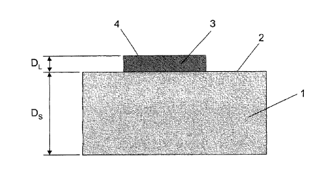
Figure 1 shows a cross-section (not to scale) through a substrate 1 of
substantially
pure aluminum or a high-purity aluminum alloy after carrying out a proposed
method. In
this case the substrate 1 comprises for example an aluminum material of the
quality EN
AW-1050A in accordance with European Standard EN 573, which contains at least
99.5%
by weight of aluminum. The substrate 1 is of a thickness Ds of about 2 mm and
has a
substantially flat surface 2. In general the substrate 1 can be of a thickness
Ds of at least
1 mm while a maximum reasonable thickness Ds can be limited by further
processing of
the substrate 1.
CA 02871937 2014-10-29
0
8
A copper-based conductor paste 3 was applied to the surface 2 of the substrate
1
by means of a screen printing process, that is to say the conductor paste 3
used contains
a copper powder as the electrically conductive constituent. The substrate 1
together with
the conductor paste 3 was treated in accordance with a proposed method using
the firing
profile of Figure 2 to obtain a solderable aluminum substrate 1. The thickness
DL of the
fired or sintered conductor paste 3 after using the proposed method is about
35pm in this
example. The thickness DL of the fired or sintered conductor paste can be for
example
between about 20pm and about 40pm for copper conductor track pastes and
between
about 10pm and about 20pm for silver conductor track pastes. To improve the
soldering
properties of the conductor paste 3 which was fired or sintered in the
proposed method
the surface 4 of the sintered conductor paste 3 was mechanically post-treated,
for
example brushed.
Figure 2 shows a possible firing profile for the proposed method. In this
respect
the illustrated diagram represents the variation in respect of time of the
firing temperature
T in a firing furnace, in which the first firing phase E31, the second firing
phase B2 and the
cooling phase A were carried out. In the first firing phase 131, starting from
an ambient
temperature of about 22 C, the firing temperature T was continuously increased
to a
predeterminable maximum firing temperature Tmax of about 542 C. The variation
in
respect of time of the firing temperature T in the first firing phase B1 is in
this case
substantially S-shaped with a substantially linear portion in which the firing
temperature T
was increased at a rate RB of about 46 C/min.
After reaching the predeterminable maximum firing temperature Tmax the
conductor
paste 3 and the substrate 1 were exposed in the second firing = phase B2 to
the
predeterminable maximum firing temperature Tr, of about 542 C for a
predeterminable
period tB of about 9 min, and thus the conductor paste 3 was fired or
sintered.
In the following cooling phase A the firing temperature T was continuously
reduced, wherein the firing temperature T decreases in relation to time t in a
substantially
S-shaped configuration. The reduction rate RA of the firing temperature T in
the cooling
phase A was approximately on average about 33 C/min.