Note: Descriptions are shown in the official language in which they were submitted.
CA 02872729 2015-06-25
1
WIRELESS, MOTION AND POSITION-SENSING, INTEGRATING
RADIATION SENSOR FOR OCCUPATIONAL AND ENVIRONMENTAL
DO SIMETRY
BACKGROUND
Field of the Invention
The present invention relates to detection systems and networks of detectors
and, particularly, to the design of a sensor system capable of detecting and
quantifying a measurable event, such as an exposure to ionizing radiation, by
recording the time, location, ambient temperature, motion and intensity of the
event;
accurately calculating the equivalent absorbed dose due to the radiation
event;
mapping the distribution of events by using data collected from a large number
of
sensor systems over a wireless network; and predicting the probable severity
of the
event by analysis of the collected sensor network data.
Background of the Invention
Occupational radiation exposure events can occur in healthcare, the oil and
gas industry, the military and other industrial settings where the use of
materials or
devices that emit ionizing radiation can result in accidental or
occupationally
unavoidable exposure events.
Emergency radiation evwsure events can occur when a Radiological
Dispersal Device (RDD), Improvised Nuclear Device (IND), or another source of
radioactive material is released and contaminates a given area.
Radiation dosimetry programs have been developed to monitor and protect
workers who might be exposed to radiation. The personal dose equivalent,
measured
using a radiation
REPLACEMENT SHEET
CA 02872729 2014-11-27
WO 2013/179273
PCT/1B2013/054517
2
dosimeter, is commonly used to monitor radiation dose to an individual. The
accurate and
reliable measurement of the personal dose equivalent from a radiation exposure
event is a key
component of radiation dosimetry. The personal dose equivalent is typically
measured over a
wide range of energies and from different radiation sources, which might
include x-rays,
gamma rays, alpha particles, beta particles and neutrons. In order to
accurately estimate the
dose from different radiation sources, many personal dosimeters incorporate an
array of
detector elements, each with varying types of radiation filtration materials,
and use a dose
calculation algorithm to accurately calculate the personal dose equivalent
from a numerical
combination of the responses from each detector element.
More recently, emergency management plans have been developed to enable the
safe
and timely response to emergency radiation events. An important aspect of any
emergency
management plan following a radiation event is to ensure the safety of fire,
police and other
emergency response personnel ("First Responders"), health-care workers, and
citizens that
might be exposed to radiation resulting from the radiological or nuclear
device. Radiation
exposure of first responders and health-care workers is often, at least
partially, monitored
using traditional radiation detecting devices, however, monitoring the
exposure of potentially
tens of thousands of citizens presents a more difficult problem.
Furthermore, after removable contamination has been eliminated, there may be a
need
for external personal dosimetry monitoring for individual members of the
public as well as
large numbers of workers. Site restoration could be a lengthy project and, to
minimize
disruption to society, it may be necessary to allow inhabitants to have access
to certain areas
before cleanup is complete. For example, allowing citizens to pass through
transit centers,
thoroughfares, or certain areas of buildings would facilitate government
operations,
commerce, uniting of families, routine medical treatments, etc. As an
individual moves
through a contaminated area, it would be valuable to know the dose and time of
exposure at
each location visited. Such dose measurements could reduce reliance on model-
based
estimates of dose, and avoid unnecessary area restrictions by providing a
geographic map of
the dynamic dose distribution reconstructed from a large number of dosimeters
collecting
dose event data over the potentially still-contaminated area.
Unlike cleanup at
decommissioned facilities where the public could be excluded with little cost
to society, in an
urban environment, time is of the essence and the cost of exclusion may be
greater than the
benefit avoiding exposure to a relatively low radiation dose. After cleanup,
personal
CA 02872729 2014-11-27
WO 2013/179273
PCT/1B2013/054517
3
dosimetry could boost public confidence that their personal dose is below
acceptable
thresholds, and that the final cleanup was effective.
In the case of radiation events, several radiation measurement technologies
currently
exist including TLD dosimeters, OSL dosimeters, electronic dosimeters, quartz
or carbon
fiber electrets, and other solid-state radiation measurement devices.
Thermoluminescent Dosimeter (TLD) badges are personal monitoring devices using
a
special material (i.e. lithium fluoride) that retains deposited energy from
radiation. TLD
badges are read using heat, which causes the TLD material to emit light that
is detected by a
TLD reader (calibrated to provide a proportional electric current).
Significant disadvantages
of TLD badges are that the signal of the device is erased or zeroed out during
read-out,
substantial time is required to obtain the reading, and the dosimeters must be
returned to a
processing laboratory for readout.
Optically Stimulated Luminescence (OSL) badges use an optically stimulated
luminescent material (OSLM) (i.e., aluminum oxide) to retain radiation energy.
Tiny crystal
traps within the OSL material trap and store energy from radiation exposure.
The amount of
exposure is determined by illuminating the crystal traps with a stimulating
light of one color
(i.e., green) and measuring the amount of emitted light of another color
(i.e., blue).
Alternatively, pulsed light stimulation can be used to differentiate between
the stimulation
and emission light [e.g., see U.S. Pat. Nos. 5,892,234 and 5,962,857. Unlike
TLD systems,
OSL systems provide a readout in only a few seconds and, because only a very
small fraction
of the exposure signal is depleted during readout, the dosimeters can be
readout multiple
times. OSL dosimeters can be read in the field using small, field-
transportable readers,
however, the readers are still too large, slow and expensive to allow
individual, real-time
readings in the field. In currently-existing OSL dosimetry programs for
reporting the dose of
record, the dosimeters must be returned to a processing laboratory for
readout.
Optically Stimulated Luminescence (OSL) badges use an optically stimulated
luminescent material (OSLM) (i.e., aluminum oxide) to retain radiation energy.
Tiny crystal
traps within the OSL material trap and store energy from radiation exposure.
The amount of
exposure is determined by illuminating the crystal traps with a stimulating
light of one color
(i.e., green) and measuring the amount of emitted light of another color
(i.e., blue).
Alternatively, pulsed light stimulation can be used to differentiate between
the stimulation
and emission light [e.g., see U.S. Pat. Nos. 5,892,234 and 5,962,857. Unlike
TLD systems,
CA 02872729 2015-06-25
4
OSL systems provide a readout in only a few seconds and, because only a very
small fraction
of the exposure signal is depleted during readout, the dosimeters can be
readout multiple
times. OSL dosimeters can be read in the field using small, field-
transportable readers,
however, the readers are still too large, slow and expensive to allow
individual, real-time
readings in the field. In currently-existing OSL dosimetry programs for
reporting the dose of
record, the dosimeters must be retarned to a processing laboratory for
readout. For more
information on OSL materials and systems, see, U.S. Pat. No. 5,731,590 issued
to Miller;
U.S. Pat. No. 6,846,434 issued to Akselrod; U.S. Pat. No. 6,198,108 issued to
Schwietzer et
al.; U.S. Pat. No. 6,127,685 issued to Yoder et al.; U.S. patent application
Ser. No.
10/768,094 filed by Akselrod et al. See also, Optically Stimulated
Luminescence Dosimetry,
Lars Bolter- Jensen et al., Elesevier, 2003; Klemic, G., Bailey, P., Miller,
K., Monetti, M.
External radiation dosimetry in the aftermath of radiological terrorist event,
Rad. Prot. Dosim,
in press; Akslerod, M. S., Kortov, V. S., and Gorelova, E. A., Preparation and
properties of
A1203:C. Radiat. Prot Dosim 47, 159-164 (1993); and Akselrod, M. S., Lucas, A.
C., Polf, J.
C., McKeever, S. W. S. Optically stimulated luminescence of A1203:C. Radiation
Measurements, 29, (3-4), 391-399 (1998).
Solid State Sensors use solid-phase materials such as semiconductors to
quantify
radiation interaction through the collection of charge in the semiconductor
media. As the
radiation particle travels through the semiconductor media electron-hole pairs
are generated
along the particle path. The motion of the electron-hole pair in an applied
electric field
generates the basic electrical signal from the detector. There are two main
categories of solid
state sensors, active and passive. Active sensors often use a semiconductor
that is biased by
an externally powered electric field that requires constant power. The active
sensors generate
electric pulses for each radioactive particle striking the sensor. These
pulses must be
continuously counted to record the correct radiation dose. A loss of power
means no dose is
measured. Active solid state sensors arc typically made from silicon and other
semiconductors. Passive solid state sensors utilize an on device charged
medium that
maintains the electric field necessary to separate the electron-hole pairs
without drawing
external power. Passive solid state dosimeters often use what is called a
floating gate where
the gate is embedded within the detection medium so it electronically
isolated. The floating
gate is charged and provides the electric field for charge separation. See
U.S. Pat. 6,172,368
issued to Tarr. The medium above the floating gate is typically an insulator
such as silicon
REPLACEMENT SHEET
CA 02872729 2014-11-27
WO 2013/179273
PCT/1B2013/054517
oxide however it can also be a sealed gas chamber. See U.S. Pat. 5,739,541
issued to
Kahilainen. Passive Solid state electronic detectors offer a means of
monitoring radiation
that are compatible the present invention.
Electronic dosimeters are battery powered, and typically incorporate a digital
display
5 or other
visual, audio or vibration alarming capability. These instruments often
provide real-
time dose rate information to the wearer. For routine occupational radiation
settings in the
U.S. electronic dosimeters are mostly, but not strictly, used for access
control and not for
dose of record. A number of cities and states issue electronic dosimeters to
HAZMAT teams
as part of their emergency response plans. There are presently tens of
thousands of electronic
dosimeters deployed, for example, for homeland security purposes, however,
electronic
dosimeters are impractical for widespread use dosimetersdue to their high
cost.
Quartz or carbon fiber electrets are cylindrical electroscopes where the dose
is read by
holding it up to the light and viewing the location of the fiber on a scale
through an eyepiece
at one end. A manually powered charger is needed to zero the dosimeter. The
quartz fiber
electret is an important element of many state emergency plans. For example,
some plans
call for emergency responders to be issued a quartz fiber electret along with
a card for
recording the reading every 30 minutes, as well as a cumulative dosimetry
badge or wallet
card. While they are specified for use in nuclear power plant emergencies, the
NRC does not
require them to be NVLAP accredited, only that they be calibrated
periodically.
Existing passive personal radiation monitoring devices do not provide
immediate
access to recorded dose measurements, while active devices typically consume
sufficient
power to require regular recharging. No existing devices measure the complete
"radiation
event."
In general, a need exists for "event detection" devices, e.g., radiation
dosimeters or
other detection devices, with the following characteristics: (1) small and
easily carried or
mounted to fixed structures or mobile transports; (2) capable of measuring a
dose event,
including the measured amplitude or intensity of the event, time of the event,
location of the
event, ambient temperature, motion of the detector and proximity to other
detectors; (3)
accurate calculation of the dose, e.g., the Personal Dose Equivalent, over a
wide dose range,
wide energy range, and large angles of incidence; (4) ability to display the
measured dose
event on the detector, or using a personal mobile device, in order to alert
the User to
anomalous events, and in order to transmit the measured dose over private and
public
CA 02872729 2014-11-27
WO 2013/179273
PCT/1B2013/054517
6
networks to a dose event repository; (5) ability to track and report dose
events in the field
over extended periods of time without replacing or externally charging the
power source; (6)
ability to map the distribution of dose over a geographic area, to identify
anomalous dose
distributions, to dynamically track sources and to alert Authorized Personnel
of anomalous
dose events.
SUMMARY
According to a first broad aspect, the present invention provides a device
comprising
a radiation sensor array comprising one or more radiation sensors mounted on a
printed
circuit board (PCB), wherein the one Of more radiation sensors are surrounded
by a filter
material to provide an optimal angular response.
According to a second broad aspect, the present invention provides an
integrated
sensor module comprising a radiation sensor array, an on-board motion sensor,
an on-board
geospatial positioning sensor, an on-board power harvester, an on-board
wireless transmitter,
and an on-board temperature sensor.
According to a third broad aspect, the present invention provides an
integrated sensor
module comprising a radiation sensor array, an on-board motion sensor, an on-
board
geospatial positioning sensor, an on-board power harvester, an on-board
wireless transmitter
and an on-board temperature sensor.
According to a fourth broad aspect, the present invention provides an an
autonomous
mobile sensor network for tracking a position and distribution of materials
comprising an
integrated sensor module comprising a radiation sensor array, an on-board
motion sensor, an
on-board geospatial positioning sensor, an on-board power harvester, an on-
board wireless
transmitter, and an on-board temperature sensor. The autonomous mobile sensor
network
may also include a communication device, a wireless network, a public data
network, and a
remote data server, wherein the communication device is configured to
communicate with the
integrated sensor module and the wireless network; wherein the wireless
network is also
configured to communicate with the public data network; and wherein the public
data
network is also configured to communicate with the remote data server.
According to a fifth broad aspect, the present invention provides an
autonomous
mobile wireless sensor base station network for tracking a position and
distribution of
CA 02872729 2014-11-27
WO 2013/179273
PCT/1B2013/054517
7
materials comprising an integrated sensor module comprising a radiation sensor
array, an on-
board motion sensor, an on-board geospatial positioning sensor, an on-board
power harvester,
an on-board wireless transmitter and an on-board temperature sensor. The
autonomous
mobile wireless sensor base station network a wireless sensor base station, a
wireless
network, a public data network and a distributed data server, wherein the
wireless sensor base
station is configured to communicate with the integrated sensor module and the
wireless
network; wherein the wireless network is also configured to communicate with
the public
data network; and wherein the public data network is also configured to
communicate with
the distributed data server.
BRIEF DESCRIPTION OF THE DRAWINGS
The accompanying drawings, which are incorporated herein and constitute part
of this
specification, illustrate exemplary embodiments of the invention, and,
together with the
general description given above and the detailed description given below,
serve to explain the
features of the invention.
FIG. 1 illustrates a split sphere encapsulating "filtration bubble" for a
plurality of
ionizing radiation sensors according to an exemplary embodiment of the present
invention;
FIG. 2 illustrates an integrated sensor module according to an exemplary
embodiment
of the present invention;
FIG. 3 illustrates a remote sensor network according to an exemplary
embodiment of
the present invention;
FIG. 4 illustrates an autonomous mobile sensor (AMS) network according to an
exemplary embodiment of the present invention;
FIG. 5 illustrates an integrated sensor module logic flow according to an
exemplary
embodiment of the present invention;
FIG. 6 illustrates a sensor readout logic flow according to an exemplary
embodiment
of the present invention;
FIG. 7 illustrates a point of exposure readout logic flow according to an
exemplary
embodiment of the present invention;
CA 02872729 2014-11-27
WO 2013/179273
PCT/1B2013/054517
8
FIG. 8 illustrates a wireless sensor base station configuration according to
an
exemplary embodiment of the present invention;
FIG. 9 illustrates a computational procedure according to an exemplary
embodiment
of the present invention;
FIG. 10 illustrates a flowchart of the disclosed computational procedure for
employing an algorithm according to an exemplary embodiment of the present
invention.
DETAILED DESCRIPTION OF THE PREFERRED EMBODIMENTS
Definitions
Where the definition of terms departs from the commonly used meaning of the
term,
applicant intends to utilize the definitions provided below, unless
specifically indicated.
For the purposes of the present invention, directional terms such as "top",
"bottom",
"upper", "lower", "above", "below", "left", "right", "horizontal", "vertical",
"upward",
"downward", etc., are merely used for convenience in describing the various
embodiments of
the present invention.
For the purposes of the present invention, the term "accelerometer" refers to
an
electromechanical device for measuring acceleration forces including static or
dynamic
forces. An accelerometer measures proper acceleration, which is the
acceleration it
experiences relative to free fall and is the acceleration felt by people and
objects. Put another
way, at any point in space time the equivalence principle guarantees the
existence of a local
inertial frame, and an accelerometer measures the acceleration relative to
that frame.[1] Such
accelerations are popularly measured in terms of g-force. Single- and multi-
axis models of
accelerometer are available to detect magnitude and direction of the proper
acceleration (or g-
force), as a vector quantity, and can be used to sense orientation (because
direction of weight
changes), coordinate acceleration (so long as it produces g-force or a change
in g-force),
vibration, shock, and falling in a resistive medium (a case where the proper
acceleration
changes, since it starts at zero, then increases). Micro-machined
accelerometers are
increasingly present in portable electronic devices and video game
controllers, to detect the
position of the device or provide for game input. Pairs of accelerometers
extended over a
region of space can be used to detect differences (gradients) in the proper
accelerations of
frames of references associated with those points. These devices are called
gravity
CA 02872729 2014-11-27
WO 2013/179273
PCT/1B2013/054517
9
gradiometers, as they measure gradients in the gravitational field. Such pairs
of
accelerometers in theory may also be able to detect gravitational waves.
For the purposes of the present invention, the term "angle of incidence"
refers to the
angle between the direction of the radiation trajectory and a line
perpendicular (normal) to the
detector surface.
For the purposes of the present invention, the term "autonomous mobile sensor
(AMS) network" refers a network of independently functioning mobile sensors,
each capable
of moving in response to the intensity of the detected event and their
proximity to the other
mobile sensors, such that the group of mobile sensors automatically follows
the dynamic
distribution of the tracked entity as the intensity changes over time or
distributes over a
geographic region or within a building or structure.
For the purposes of the present invention, the term "ANT" or "ANT+' refers to
a proprietary wireless sensor network technology featuring a
wireless
communications protocol stack that enables semiconductor radios operating in
the
2.4 GHz industrial, scientific, and medical allocation of the RF spectrum
("ISM band") to
communicate by establishing standard rules for co-existence, data
representation,
signaling, authentication, and error detection. ANT is characterized by a low
computational
overhead and low to medium efficiency, resulting in low power consumption by
the radios
supporting the protocol.
For the purposes of the present invention, the term "Bluetooth0" refers to a
wireless
technology standard for exchanging data over short distances (using short-
wavelength radio
transmissions in the ISM band from 2400-2480 MHz) from fixed and mobile
devices,
creating personal area networks (PANs) with high levels of security. Created
by telecom
vendor Ericsson in 1994, it was originally conceived as a wireless alternative
to RS-232 data
cables. It can connect several devices, overcoming problems of
synchronization. Bluetooth0
is managed by the Bluetooth0 Special Interest Group, which has more than
18,000 member
companies in the areas of telecommunication, computing, networking, and
consumer
electronics. Bluetooth0 was standardized as IEEE 802.15.1, but the standard is
no longer
maintained. The SIG oversees the development of the specification, manages the
qualification program, and protects the trademarks. To be marketed as a
Bluetooth0 device,
it must be qualified to standards defined by the SIG. A network of patents is
required to
implement the technology and are licensed only for those qualifying devices.
CA 02872729 2014-11-27
WO 2013/179273
PCT/1B2013/054517
For the purposes of the present invention, the term a "chemical sensor" refers
to a
device that measures the presence, concentration or absolute quantity of a
given chemical
entity, such as an element or molecule, in either a gas, liquid or solid
phase.
For the purposes of the present invention, the term "cloud computing" is
synonymous
5 with computing performed by computers that are located remotely and
accessed via the
Internet (the "Cloud"). It is a style of computing where the computing
resources are provided
"as a service", allowing users to access technology-enabled services "in the
cloud" without
knowledge of, expertise with, or control over the technology infrastructure
that supports
them. According to the IEEE Computer Society it "is a paradigm in which
information is
10 permanently stored in servers on the Internet and cached temporarily on
clients that include
desktops, entertainment centers, table computers, notebooks, wall computers,
handhelds, etc."
Cloud computing is a general concept that incorporates virtualized storage,
computing and
web services and, often, software as a service (SaaS), where the common theme
is reliance on
the Internet for satisfying the computing needs of the users. For example,
Google Apps
provides common business applications online that are accessed from a web
browser, while
the software and data are stored on the servers. Some successful cloud
architectures may
have little or no established infrastructure or billing systems whatsoever
including Peer-to-
peer networks like BitTorrent and Skype and volunteer computing like
SETI@home. The
majority of cloud computing infrastructure currently consists of reliable
services delivered
through next-generation data centers that are built on computer and storage
virtualization
technologies. The services may be accessible anywhere in the world, with the
Cloud
appearing as a single point of access for all the computing needs of data
consumers.
Commercial offerings may need to meet the quality of service requirements of
customers and
may offer service level agreements. Open standards and open source software
are also
critical to the growth of cloud computing. As customers generally do not own
the
infrastructure, they are merely accessing or renting, they may forego capital
expenditure and
consume resources as a service, paying instead for what they use. Many cloud
computing
offerings have adopted the utility computing model which is analogous to how
traditional
utilities like electricity are consumed, while others are billed on a
subscription basis. By
sharing "perishable and intangible" computing power between multiple tenants,
utilization
rates may be improved (as servers are not left idle) which can reduce costs
significantly while
increasing the speed of application development. A side effect of this
approach is that
"computer capacity rises dramatically" as customers may not have to engineer
for peak loads.
CA 02872729 2014-11-27
WO 2013/179273
PCT/1B2013/054517
11
Adoption has been enabled by "increased high-speed bandwidth" which makes it
possible to
receive the same response times from centralized infrastructure at other
sites.
For the purposes of the present invention, the term "computer" refers to a
machine
that manipulates data according to a sequence of instructions stored on a
machine readable
medium. A computer may include one or more processors that that execute such a
sequence
of instructions to cause one or more electronic devices, often including the
computer itself, to
perform a set of operations. Personal computers, in various forms, are icons
of the
Information Age and are what most people think of as a "computer"; however,
the most
common form of computer in use today is the embedded computer. Embedded
computers are
small, simple devices that are used to control other devices ¨ for example,
they may be
found in machines ranging from fighter aircraft to industrial robots, digital
cameras, and
children's toys. The ability to store and execute lists of instructions called
programs makes
computers extremely versatile and distinguishes them from calculators. The
Church¨Turing
thesis is a mathematical statement of this versatility: any computer with a
certain minimum
capability is, in principle, capable of performing the same tasks that any
other computer can
perform. Therefore, computers with capability and complexity ranging from that
of a
personal digital assistant to a supercomputer are all able to perform the same
computational
tasks given enough time and storage capacity. Computers are indispensable for
the analysis
of large amounts of data, for tasks that require complex computation, or for
the extraction of
quantitative information.
For the purposes of the present invention, the term "computer hardware" is the
digital
circuitry and physical devices of a computer system, as opposed to computer
software, which
is stored on a hardware device such as a hard disk. Most computer hardware is
not seen by
normal users, because it is embedded within a variety of every day systems,
such as in
automobiles, microwave ovens, electrocardiograph machines, compact disc
players, and
video games, among many others. A typical personal computer consists of a case
or chassis
in a tower shape (desktop) and the following parts: motherboard, CPU, RAM,
firmware,
internal buses (PIC, PCI-E, USB, HyperTransport, CSI, AGP, VLB), external bus
controllers
(parallel port, serial port, USB, Firewire, SCSI. PS/2, ISA, EISA, MCA), power
supply, case
control with cooling fan, storage controllers (CD-ROM, DVD, DVD-ROM, DVD
Writer,
DVD RAM Drive, Blu-ray, BD-ROM, BD Writer, floppy disk, USB Flash, tape
drives,
SATA, SAS), video controller, sound card, network controllers (modem, NIC),
and
CA 02872729 2014-11-27
WO 2013/179273
PCT/1B2013/054517
12
peripherals, including mice, keyboards, pointing devices, gaming devices,
scanner, webcam,
audio devices, printers, monitors, etc.
For the purposes of the present invention, the term "computer network" refers
to a
group of interconnected computers. Networks may be classified according to a
wide variety
of characteristics. The most common types of computer networks in order of
scale include:
Personal Area Network (PAN), Local Area Network (LAN), Campus Area Network
(CAN),
Metropolitan Area Network (MAN), Wide Area Network (WAN), Global Area Network
(GAN), Intemetwork (intranet, extranet, Internet), and various types of
wireless networks.
All networks are made up of basic hardware building blocks to interconnect
network nodes,
such as Network Interface Cards (NICs), Bridges, Hubs, Switches, and Routers.
In addition,
some method of connecting these building blocks is required, usually in the
form of galvanic
cable (most commonly category 5 cable). Less common are microwave links (as in
IEEE
802.11) or optical cable ("optical fiber").
For the purposes of the present invention, the term "computer software" refers
to a
general term used to describe a collection of computer programs, procedures
and
documentation that perform some tasks on a computer system. The term includes
application
software such as word processors which perform productive tasks for users,
system software
such as operating systems, which interface with hardware to provide the
necessary services
for application software, and middleware which controls and co-ordinates
distributed
systems. Software may include websites, programs, video games, etc. that are
coded by
programming languages like C, C++, Java, etc. Computer software is usually
regarded as
anything but hardware, meaning the "hard" are the parts that are tangible
(able to hold) while
the "soft" part is the intangible objects inside the computer. Computer
software is so called
to distinguish it from computer hardware, which encompasses the physical
interconnections
and devices required to store and execute (or run) the software. At the lowest
level, software
consists of a machine language specific to an individual processor. A machine
language
consists of groups of binary values signifying processor instructions which
change the state
of the computer from its preceding state.
For the purposes of the present invention, the term "computer system" refers
to any
type of computer system that implements software including an individual
computer such as
a personal computer, mainframe computer, mini-computer, etc. In addition,
computer system
refers to any type of network of computers, such as a network of computers in
a business, the
CA 02872729 2014-11-27
WO 2013/179273
PCT/1B2013/054517
13
Internet, personal data assistant (PDA), devices such as a cell phone, a
television, a
videogame console, a compressed audio or video player such as an MP3 player, a
DVD
player, a microwave oven, etc. A personal computer is one type of computer
system that
typically includes the following components: a case or chassis in a tower
shape (desktop)
and the following parts: motherboard, CPU, RAM, firmware, internal buses (PIC,
PCI-E,
USB, HyperTransport, CSI, AGP, VLB), external bus controllers (parallel port,
serial port,
USB, Firewire, SCSI. PS/2, ISA, EISA, MCA), power supply, case control with
cooling fan,
storage controllers (CD-ROM, DVD, DVD-ROM, DVD Writer, DVD RAM Drive, Blu-ray,
BD-ROM, BD Writer, floppy disk, USB Flash, tape drives, SATA, SAS), video
controller,
sound card, network controllers (modem, NIC), and peripherals, including mice,
keyboards,
pointing devices, gaming devices, scanner, webcam, audio devices, printers,
monitors, etc.
For the purposes of the present invention, the term "data" means the
reinterpretable
representation of information in a formalized manner suitable for
communication,
interpretation, or processing. Although one type of common type data is a
computer file, data
may also be streaming data, a web service, etc. The term "data" is used to
refer to one or
more pieces of data.
For the purposes of the present invention, the term "database" or "data
record" refers
to a structured collection of records or data that is stored in a computer
system. The structure
is achieved by organizing the data according to a database model. The model in
most
common use today is the relational model. Other models such as the
hierarchical model and
the network model use a more explicit representation of relationchips (see
below for
explanation of the various database models). A computer database relies upon
software to
organize the storage of data. This software is known as a database management
system
(DBMS). Database management systems are categorized according to the database
model
that they support. The model tends to determine the query languages that are
available to
access the database. A great deal of the internal engineering of a DBMS,
however, is
independent of the data model, and is concerned with managing factors such as
performance,
concurrency, integrity, and recovery from hardware failures. In these areas
there are large
differences between products.
For the purposes of the present invention, the term "database management
system
(DBMS)" represents computer software designed for the purpose of managing
databases
based on a variety of data models. A DBMS is a set of software programs that
controls the
CA 02872729 2014-11-27
WO 2013/179273
PCT/1B2013/054517
14
organization, storage, management, and retrieval of data in a database. DBMS
are
categorized according to their data structures or types. It is a set of
prewritten programs that
are used to store, update and retrieve a Database.
For the purposes of the present invention, the term "data storage medium" or
"data
storage device" refers to any medium or media on which a data may be stored
for use by a
computer system. Examples of data storage media include floppy disks, ZipTM
disks, CD-
ROM, CD-R, CD-RW, DVD, DVD-R, memory sticks, flash memory, hard disks, solid
state
disks, optical disks, etc. Two or more data storage media acting similarly to
a single data
storage medium may be referred to as a "data storage medium" for the purposes
of the
present invention.
For the purposes of the present invention, the term "dosimeter" refers to a
device for
measuring an individual's or an object's exposure to something in the
environment ¨
particularly to a hazard inflicting cumulative impact over long periods of
time, or over a
lifetime. This article concentrates on the radiation dosimeter, which measures
exposure to
ionizing radiation. The radiation dosimeter is of fundamental importance in
the disciplines of
radiation dosimetry and health physics. Other types of dosimeters are sound
dosimeters,
ultraviolet dosimeters and electromagnetic field dosimeters. Ionizing
radiation, such as X-
rays, alpha rays, beta rays, and gamma rays, are undetectable by the human
senses, therefore
a measuring device, such as a dosimeter, is used to detect, measure and record
this, and in
some cases give an alarm when a preset level is exceeded. Ionizing radiation
damage to the
body is cumulative, and is related to the total dose received, for which the
SI unit is the
sievert. Therefore, workers exposed to radiation, such as radiographers,
nuclear power plant
workers, doctors using radiotherapy, those in laboratories using
radionuclides, and some
HAZMAT teams are required to wear dosimeters so their employers can keep a
record of
their exposure to verify that it is below legally prescribed limits. Such
devices may be
recognized as "legal dosimeters," meaning that they have been approved for use
in recording
personnel dose for regulatory purposes.
For the purposes of the present invention, the term "energy compensating
material"
refers to a material that when placed between an OSLM and a source of gamma
radiation or
x-ray radiation alters the response over a range of gamma energies or x-ray
energies
compared to the OSLM exposed with no compensating or filtering material.
Examples of
energy compensating materials are copper and aluminum.
CA 02872729 2014-11-27
WO 2013/179273
PCT/1B2013/054517
For the purposes of the present invention, the term "flocking-algorithm"
refers to an
computational procedure that allows a network of mobile sensors to move as a
function of
each sensor's proximity to other mobile sensors as well as the intensity or
amplitude of a
measured event, such that the network of mobile sensors moves autonomously in
a concerted,
5 self-organized fashion that tracks the dynamic motion and distribution of
the measured event.
For the purposes of the present invention, the term "Internet" is a global
system of
interconnected computer networks that interchange data by packet switching
using the
standardized Internet Protocol Suite (TCP/IP). It is a "network of networks"
that consists of
millions of private and public, academic, business, and government networks of
local to
10 global scope that are linked by copper wires, fiber-optic cables,
wireless connections, and
other technologies. The Internet carries various information resources and
services, such as
electronic mail, online chat, file transfer and file sharing, online gaming,
and the inter-linked
hypertext documents and other resources of the World Wide Web (WWW).
For the purposes of the present invention, the term "Internet protocol (IP)"
refers to a
15 protocol used for communicating data across a packet-switched
internetwork using the
Internet Protocol Suite (TCP/IP). IP is the primary protocol in the Internet
Layer of the
Internet Protocol Suite and has the task of delivering datagrams (packets)
from the source
host to the destination host solely based on its address. For this purpose the
Internet Protocol
defines addressing methods and structures for datagram encapsulation. The
first major
version of addressing structure, now referred to as Internet Protocol Version
4 (Ipv4) is still
the dominant protocol of the Internet, although the successor, Internet
Protocol Version 6
(Ipv6) is actively deployed world-wide. In one embodiment, an EGI-SOA of the
present
invention may be specifically designed to seamlessly implement both of these
protocols.
For the purposes of the present invention, the term "intranet" refers to a set
of
networks, using the Internet Protocol and IP-based tools such as web browsers
and file
transfer applications that are under the control of a single administrative
entity. That
administrative entity closes the intranet to all but specific, authorized
users. Most commonly,
an intranet is the internal network of an organization. A large intranet will
typically have at
least one web server to provide users with organizational information.
Intranets may or may not have connections to the Internet. If connected to the
Internet, the
intranet is normally protected from being accessed from the Internet without
proper
authorization. The Internet is not considered to be a part of the intranet.
CA 02872729 2014-11-27
WO 2013/179273
PCT/1B2013/054517
16
For the purposes of the present invention, the term "ionizing radiation"
refers to any
particulate or electromagnetic radiation that is capable of dissociating atoms
into a positively
and negatively charged ion pair. The present invention may be used to
determine doses of
both directly ionizing radiation and indirectly ionizing radiation. Ionizing
(or ionising)
radiation is radiation composed of particles that individually carry enough
kinetic energy to
liberate an electron from an atom or molecule, ionizing it. Ionizing radiation
is generated
through nuclear reactions, either artificial or natural, by very high
temperature (e.g., plasma
discharge or the corona of the Sun), via production of high energy particles
in particle
accelerators, or due to acceleration of charged particles by the
electromagnetic fields
produced by natural processes, from lightning to supernova explosions. When
ionizing
radiation is emitted by or absorbed by an atom, it can liberate an atomic
particle (typically an
electron, proton, or neutron, but sometimes an entire nucleus) from the atom.
Such an event
can alter chemical bonds and produce ions, usually in ion-pairs, that are
especially chemically
reactive. This greatly magnifies the chemical and biological damage per unit
energy of
radiation because chemical bonds will be broken in this process. If the atom
was inside a
crystal lattice in a solid phase, then a "hole" will exist where the original
atom was. Ionizing
radiation includes cosmic rays, Alpha particles, Beta particles, Gamma rays, X-
rays, and in
general any charged particle moving at relativistic speeds. Neutrons are
considered ionizing
radiation at any speed. Ionizing radiation includes some portion of the
ultraviolet spectrum,
depending on context. Radio waves, microwaves, infrared light, and visible
light are
normally considered non-ionizing radiation, although very high intensity beams
of these
radiations can produce sufficient heat to exhibit some similar properties to
ionizing radiation,
by altering chemical bonds and removing electrons from atoms. Ionizing
radiation is
ubiquitous in the environment, and comes from naturally occurring radioactive
materials and
cosmic rays. Common artificial sources are artificially produced
radioisotopes, X-ray tubes
and particle accelerators. Ionizing radiation is invisible and not directly
detectable by human
senses, so instruments such as Geiger counters are usually required to detect
its presence. In
some cases it may lead to secondary emission of visible light upon interaction
with matter,
such as in Cherenkov radiation and radioluminescence. It has many practical
uses in
medicine, research, construction, and other areas, but presents a health
hazard if used
improperly. Exposure to ionizing radiation causes damage to living tissue, and
can result in
mutation, radiation sickness, cancer, and death.
CA 02872729 2014-11-27
WO 2013/179273
PCT/1B2013/054517
17
For the purposes of the present invention, the term "ionizing radiation
sensor" refers
to a device that measures the presence or activity of a material or substance
that emits or
generates ionizing radiation.
For the purposes of the present invention, the term "irradiation" refers to
the
conventional meaning of the term "irradiation", i.e., exposure to high energy
charge particles,
e.g., electrons, protons, alpha particles, etc., or electromagnetic radiation
of wave-lengths
shorter than those of visible light, e.g., gamma rays, x-rays, ultraviolet,
etc.
For the purposes of the present invention, the term "local area network (LAN)"
refers
to a network covering a small geographic area, like a home, office, or
building. Current
LANs are most likely to be based on Ethernet technology. The cables to the
servers are
typically on Cat 5e enhanced cable, which will support IEEE 802.3 at 1 Gbit/s.
A wireless
LAN may exist using a different IEEE protocol, 802.11b, 802.11g or possibly
802.11n. The
defining characteristics of LANs, in contrast to WANs (wide area networks),
include their
higher data transfer rates, smaller geographic range, and lack of a need for
leased
telecommunication lines. Current Ethernet or other IEEE 802.3 LAN technologies
operate at
speeds up to 10 Gbit/s.
For the purposes of the current invention, the term "low powered wireless
network"
refers to an ultra-low powered wireless network between sensor nodes and a
centralized
device. The ultra-low power is needed by devices that need to operate for
extended periods
of time from small batteries energy scavenging technology. Examples of low
powered
wireless networks are ANT, ANT+, Bluetooth Low Energy (BLE), ZigBee and WiFi.
For the purposes of the present invention, the term "MEMS" refers to Micro-
Electro-
Mechanical Systems. MEMS, is a technology that in its most general form may be
defined as
miniaturized mechanical and electro-mechanical elements (i.e., devices and
structures) that
are made using the techniques of microfabrication. The critical physical
dimensions of
MEMS devices can vary from well below one micron on the lower end of the
dimensional
spectrum, all the way to several millimeters. Likewise, the types of MEMS
devices can vary
from relatively simple structures having no moving elements, to extremely
complex
electromechanical systems with multiple moving elements under the control of
integrated
microelectronics. A main criterion of MEMS may include that there are at least
some
elements having some sort of mechanical functionality whether or not these
elements can
move. The term used to define MEMS varies in different parts of the world. In
the United
CA 02872729 2014-11-27
WO 2013/179273
PCT/1B2013/054517
18
States they are predominantly called MEMS, while in some other parts of the
world they are
called "Microsystems Technology" or "micromachined devices." While the
functional
elements of MEMS are miniaturized structures, sensors, actuators, and
microelectronics, most
notable elements may include microsensors and microactuators. Microsensors and
microactuators may be appropriately categorized as "transducers," which are
defined as
devices that convert energy from one form to another. In the case of
microsensors, the device
typically converts a measured mechanical signal into an electrical signal.
For the purposes of the present invention the term "mesh networking" refers to
a type
of networking where each node must not only capture and disseminate its own
data, but also
serve as a relay for other nodes, that is, it must collaborate to propagate
the data in the
network. A mesh network can be designed using a flooding technique or a
routing technique.
When using a routing technique, the message is propagated along a path, by
hopping from
node to node until the destination is reached. To ensure all its paths'
availability, a routing
network must allow for continuous connections and reconfiguration around
broken or
blocked paths, using self-healing algorithms. A mesh network whose nodes are
all connected
to each other is a fully connected network. Mesh networks can be seen as one
type of ad hoc
network. Mobile ad hoc networks and mesh networks are therefore closely
related, but
mobile ad hoc networks also have to deal with the problems introduced by the
mobility of the
nodes. The self-healing capability enables a routing based network to operate
when one node
breaks down or a connection goes bad. As a result, the network is typically
quite reliable, as
there is often more than one path between a source and a destination in the
network.
Although mostly used in wireless situations, this concept is also applicable
to wired networks
and software interaction.
For the purposes of the present invention the term "mobile ad hoc network" is
a self-
configuring infrastructureless network of mobile devices connected by
wireless. Ad hoc is
Latin and means "for this purpose". Each device in a mobile ad hoc network is
free to move
independently in any direction, and will therefore change its links to other
devices frequently.
Each must forward traffic unrelated to its own use, and therefore be a router.
The primary
challenge in building a mobile ad hoc network is equipping each device to
continuously
maintain the information required to properly route traffic. Such networks may
operate by
themselves or may be connected to the larger Internet. Mobile ad hoc networks
are a kind
of wireless ad hoc networks that usually has a routable networking environment
on top of
CA 02872729 2014-11-27
WO 2013/179273
PCT/1B2013/054517
19
a Link Layer ad hoc network. The growths of laptops and wireless networks have
made
mobile ad hoc networks a popular research topic since the mid-1990s. Many
academic papers
evaluate protocols and their abilities, assuming varying degrees of mobility
within a bounded
space, usually with all nodes within a few hops of each other. Different
protocols are then
evaluated based on measure such as the packet drop rate, the overhead
introduced by the
routing protocol, end-to-end packet delays, network throughput etc.
For the purposes of the present invention, the term "network hub" refers to an
electronic device that contains multiple ports. When a packet arrives at one
port, it is copied
to all the ports of the hub for transmission. When the packets are copied, the
destination
address in the frame does not change to a broadcast address. It does this in a
rudimentary
way, it simply copies the data to all of the Nodes connected to the hub. This
term is also
known as hub. The term "Ethernet hub," "active hub," "network hub," "repeater
hub,"
"multiport repeater" or "hub" may also refer to a device for connecting
multiple Ethernet
devices together and making them act as a single network segment. It has
multiple
input/output (I/0) ports, in which a signal introduced at the input of any
port appears at the
output of every port except the original incoming. A hub works at the physical
layer (layer 1)
of the OSI model. The device is a form of multiport repeater. Repeater hubs
also participate
in collision detection, forwarding a jam signal to all ports if it detects a
collision.
For the purposes of the present invention, the term "radiation attenuating
material"
refers to a material that reduces the intensity of incident radiation by
absorbing some or all of
the energy of the radiation within the material.
For the purposes of the present invention, the term "radiation dosimetry"
refers to the
conventional meaning of the term "radiation dosimetry", i.e., the measurement
of the amount
of radiation dose absorbed in a material, an object or the body of an
individual.
For the purposes of the present invention, the term "radiation sensing
material" refers
to a material used to sense radiation in a radiation sensor. Examples of
radiation sensitive
materials including optically stimulated luminescent materials for OSL
sensors,
thermoluminescent materials for thermoluminescent dosimetry (TLD) sensors,
etc.
For the purposes of the present invention, the term "random-access memory
(RAM)"
refers to a type of computer data storage. Today it takes the form of
integrated circuits that
allow the stored data to be accessed in any order, i.e. at random. The word
random thus
refers to the fact that any piece of data can be returned in a constant time,
regardless of its
CA 02872729 2014-11-27
WO 2013/179273
PCT/1B2013/054517
physical location and whether or not it is related to the previous piece of
data. This contrasts
with storage mechanisms such as tapes, magnetic discs and optical discs, which
rely on the
physical movement of the recording medium or a reading head. In these devices,
the
movement takes longer than the data transfer, and the retrieval time varies
depending on the
5 physical
location of the next item. The word RAM is mostly associated with volatile
types of
memory (such as DRAM memory modules), where the information is lost after the
power is
switched off. However, many other types of memory are RAM as well, including
most types
of ROM and a kind of flash memory called NOR-Flash.
For the purposes of the present invention, the term "read-only memory (ROM)"
refers
10 to a
class of storage media used in computers and other electronic devices. Because
data
stored in ROM cannot be modified (at least not very quickly or easily), it is
mainly used to
distribute firmware (software that is very closely tied to specific hardware,
and unlikely to
require frequent updates). In its strictest sense, ROM refers only to mask ROM
(the oldest
type of solid state ROM), which is fabricated with the desired data
permanently stored in it,
15 and thus
can never be modified. However, more modern types such as EPROM and flash
EEPROM can be erased and re-programmed multiple times; they are still
described as "read-
only memory" because the reprogramming process is generally infrequent,
comparatively
slow, and often does not permit random access writes to individual memory
locations.
For the purposes of the present invention, the term "real-time processing"
refers to a
20
processing system designed to handle workloads whose state is constantly
changing. Real-
time processing means that a transaction is processed fast enough for the
result to come back
and be acted on as transaction events are generated. In the context of a
database, real-time
databases are databases that are capable of yielding reliable responses in
real-time.
For the purposes of the present invention, the term "router" refers to a
networking
device that forwards data packets between networks using headers and
forwarding tables to
determine the best path to forward the packets. Routers work at the network
layer of the
TCP/IP model or layer 3 of the OSI model. Routers also provide
interconnectivity between
like and unlike media devices. A router is connected to at least two networks,
commonly two
LANs or WANs or a LAN and its ISP's network.
For the purposes of the present invention, the term "sensor" refers to a
collector
and/or producer of information and/or data. A sensor can be an instrument or a
living
organism (e.g. a person). For example, a sensor may be a GPS device, a
thermometer, a
CA 02872729 2014-11-27
WO 2013/179273
PCT/1B2013/054517
21
mobile phone, an individual writing a report, etc. A sensor is an entity
capable of observing a
phenomenon and returning an observed value. For example, a mercury thermometer
converts
the measured temperature into expansion and contraction of a liquid which can
be read on a
calibrated glass tube. A thermocouple converts temperature to an output
voltage which can
be read by a voltmeter. For accuracy, all sensors are often be calibrated
against known
standards. A sensor may include a device which detects or measures a physical
property and
records records, indicates, or responds to that physical property.
For the purposes of the present invention, the term "server" refers to a
system
(software and suitable computer hardware) that responds to requests across a
computer
network to provide, or help to provide, a network service. Servers can be run
on a dedicated
computer, which is also often referred to as "the server," but many networked
computers are
capable of hosting servers. In many cases, a computer can provide several
services and have
several servers running. Servers may operate within a client-server
architecture and may
comprise computer programs running to serve the requests of other programs ¨
the clients.
Thus, the server may perform some task on behalf of clients. The clients
typically connect to
the server through the network but may run on the same computer. In the
context of Internet
Protocol (IP) networking, a server is a program that operates as a socket
listener. Servers
often provide essential services across a network, either to private users
inside a large
organization or to public users via the Internet. Typical computing servers
are database
server, file server, mail server, print server, web server, gaming server,
application server, or
some other kind of server. Numerous systems use this client/server networking
model
including Web sites and email services. An alternative model, peer-to-peer
networking may
enable all computers to act as either a server or client as needed.
For the purposes of the present invention, the term "solid-state electronics"
refers to
those circuits or devices built entirely from solid materials and in which the
electrons, or
other charge carriers, are confined entirely within the solid material. The
term is often used
to contrast with the earlier technologies of vacuum and gas-discharge tube
devices and it is
also conventional to exclude electro-mechanical devices (relays, switches,
hard drives and
other devices with moving parts) from the term solid state. While solid-state
can include
crystalline, polycrystalline and amorphous solids and refer to electrical
conductors, insulators
and semiconductors, the building material is most often a crystalline
semiconductor.
Common solid-state devices include transistors, microprocessor chips, and RAM.
A
CA 02872729 2014-11-27
WO 2013/179273
PCT/1B2013/054517
22
specialized type of RAM called flash RAM is used in flash drives and more
recently, solid
state drives to replace mechanically rotating magnetic disc hard drives. More
recently, the
integrated circuit (IC), the light-emitting diode (LED), and the liquid-
crystal display (LCD)
have evolved as further examples of solid-state devices. In a solid-state
component, the
current is confined to solid elements and compounds engineered specifically to
switch and
amplify it.
For the purposes of the present invention, the term "solid state sensor"
refers to sensor
built entirely from a solid-phase material such that the electrons or other
charge carriers
produced in response to the measured quantity stay entirely with the solid
volume of the
detector, as opposed to gas-discharge or electro-mechanical sensors. Pure
solid-state sensors
have no mobile parts and are distinct from electro-mechanical transducers or
actuators in
which mechanical motion is created proportional to the measured quantity.
For purposes of the present invention, the term the term "storage medium"
refers to
any form of storage that may be used to store bits of information. Examples of
storage
include both volatile and non-volatile memories such as MRRAM, MRRAM, ERAM,
flash
memory, RFID tags, floppy disks, ZiPTM disks, CD-ROM, CD-R, CD-RW, DVD, DVD-R,
flash memory, hard disks, optical disks, etc.
For the purposes of the present invention, the term "transmission control
protocol
(TCP)" refers to one of the core protocols of the Internet Protocol Suite. TCP
is so central
that the entire suite is often referred to as "TCP/IP." Whereas IP handles
lower-level
transmissions from computer to computer as a message makes its way across the
Internet,
TCP operates at a higher level, concerned only with the two end systems, for
example a Web
browser and a Web server. In particular, TCP provides reliable, ordered
delivery of a stream
of bytes from one program on one computer to another program on another
computer.
Besides the Web, other common applications of TCP include e-mail and file
transfer. Among
its management tasks, TCP controls message size, the rate at which messages
are exchanged,
and network traffic congestion.
For the purposes of the present invention, the term "time" refers to a
component of a
measuring system used to sequence events, to compare the durations of events
and the
intervals between them, and to quantify the motions of objects. Time is
considered one of the
few fundamental quantities and is used to define quantities such as velocity.
An operational
definition of time, wherein one says that observing a certain number of
repetitions of one or
CA 02872729 2014-11-27
WO 2013/179273
PCT/1B2013/054517
23
another standard cyclical event (such as the passage of a free-swinging
pendulum) constitutes
one standard unit such as the second, has a high utility value in the conduct
of both advanced
experiments and everyday affairs of life. Temporal measurement has occupied
scientists and
technologists, and was a prime motivation in navigation and astronomy.
Periodic events and
periodic motion have long served as standards for units of time. Examples
include the
apparent motion of the sun across the sky, the phases of the moon, the swing
of a pendulum,
and the beat of a heart. Currently, the international unit of time, the
second, is defined in
terms of radiation emitted by cesium atoms.
For the purposes of the present invention, the term "timestamp" refers to a
sequence
of characters, denoting the date and/or time at which a certain event
occurred. This data is
usually presented in a consistent format, allowing for easy comparison of two
different
records and tracking progress over time; the practice of recording timestamps
in a consistent
manner along with the actual data is called timestamping. Timestamps are
typically used for
logging events, in which case each event in a log is marked with a timestamp.
In file
systems, timestamp may mean the stored date/time of creation or modification
of a file. The
International Organization for Standardization (ISO) has defined ISO 8601
which
standardizes timestamps.
For the purposes of the present invention, the term "visual display device" or
"visual
display apparatus" includes any type of visual display device or apparatus
such as a CRT
monitor, LCD screen, LEDs, a projected display, a printer for printing out an
image such as a
picture and/or text, etc. A visual display device may be a part of another
device such as a
computer monitor, television, projector, telephone, cell phone, smartphone,
laptop computer,
tablet computer, handheld music and/or video player, personal data assistant
(PDA), handheld
game player, head mounted display, a heads-up display (HUD), a global
positioning system
(GPS) receiver, automotive navigation system, dashboard, watch, microwave
oven, electronic
organ, automatic teller machine (ATM) etc.
For the purposes of the present invention, the term "web service" refers to
the term
defined by the W3C as "a software system designed to support interoperable
machine-to-
machine interaction over a network". Web services are frequently just web APIs
that can be
accessed over a network, such as the Internet, and executed on a remote system
hosting the
requested services. The W3C Web service definition encompasses many different
systems,
but in common usage the term refers to clients and servers that communicate
using XML
CA 02872729 2014-11-27
WO 2013/179273
PCT/1B2013/054517
24
messages that follow the SOAP standard. In such systems, there is often
machine-readable
description of the operations offered by the service written in the Web
Services Description
Language (WSDL). The latter is not a requirement of a SOAP endpoint, but it is
a
prerequisite for automated client-side code generation in many Java and .NET
SOAP
frameworks. Some industry organizations, such as the WS-I, mandate both SOAP
and
WSDL in their definition of a Web
service.
More recently, RESTful Web services have been regaining popularity. These also
meet the
W3C definition, and are often better integrated with HTTP than SOAP-based
services. They
do not require XML messages or WSDL service-API definitions.
For the purposes of the present invention, the term "wide area network (WAN)"
refers to a data communications network that covers a relatively broad
geographic area (i.e.
one city to another and one country to another country) and that often uses
transmission
facilities provided by common carriers, such as telephone companies. WAN
technologies
generally function at the lower three layers of the OSI reference model: the
physical layer, the
data link layer, and the network layer.
For the purposes of the present invention, the term "World Wide Web Consortium
(W3C)" refers to the main international standards organization for the World
Wide Web
(abbreviated WWW or W3). It is arranged as a consortium where member
organizations
maintain full-time staff for the purpose of working together in the
development of standards
for the World Wide Web. W3C also engages in education and outreach, develops
software
and serves as an open forum for discussion about the Web. W3C standards
include:
CSS, CGI, DOM, GRDDL, HTML, OWL, RDF, SVG, SISR, SOAP, SMIL, SRGS, SSML,
VoiceXML, XHTML+Voice, WSDL, XACML. XHTML, XML, XML Events, Xforms,
XML Information, Set, XML Schema, Xpath, Xquery and XSLT.
For the purposes of the present invention, the term "ZigBee" refers a
specification for
a suite of high level communication protocols used to create personal area
networks built
from small, low-power digital radios. ZigBee is based on an IEEE 802 standard.
Though
low-powered, ZigBee devices often transmit data over longer distances by
passing data
through intermediate devices to reach more distant ones, creating a mesh
network; i.e., a
network with no centralized control or high-power transmitter/receiver able to
reach all of the
networked devices. The decentralized nature of such wireless ad-hoc networks
make them
suitable for applications where a central node can't be relied upon. ZigBee
may be used in
CA 02872729 2015-06-25
applications that require a low data rate, long battery life, and secure
networking. ZigBee has
a defined rate of 250 kbit/s, best suited for periodic or intermittent data or
a single signal
transmission from a sensor or input device. Applications include wireless
light switches,
electrical meters with in-home-displays, traffic management systems, and other
consumer and
5 industrial
equipment that requires short-range wireless transfer of data at relatively
low rates.
The technology defined by the ZigBee specification is intended to be simpler
and less
expensive than other WPANs, such as Bluetooth0 or Wi-Fi. Zigbee networks are
secured by
128 bit encryption keys.
Description
10 In existing
passive, integrating radiation monitoring devices, such as film, TLD or
OSL sensors, incident radiation is accumulated and stored within the molecular
structure of
the sensor without any need of electrical power. This characteristic makes
passive sensors
ideal for situations where the risk of a power interruption is unacceptable.
Multiple radiation
sensors are generally mounted in a holder containing one or more filters that
alter the
15 amounts,
energies and types of radiation able to reach the sensors. These filters
typically
sandwich the sensors to achieve correct assessments when the radiation enters
the dosimeter
from various angles of incidence. To analyze the sensors, they must be removed
from
between the filters and the holder and physically presented to the processing
system required
to elicit the quantitative attribute exhibited by the sensor following
exposure to radiation.
20 Radiation
dosimeters based on optically stimulated luminescence (OSL) utilize an
optical path whereby a stimulating beam of light can illuminate the OSL
sensor(s) and thc
resultant radiation induced luminescence can be routed back through the same
or alternate
optical path to a light detector such as a photomultiplier tube that
quantifies the amount of
luminescent light. For more information on OSL materials and systems, see,
U.S. Pat. No.
25 5,731,590
issued to Miller; U.S. Pat. No. 6,846,434 issued to Akselrod; U.S. Pat. No.
6,198,108 issued to Schweitzer et al.; U.S. Pat. No. 6,127,685 issued to Yoder
et al.; U.S.
patent application Ser. No. 10/768,094 filed by Akselrod et al. See also
Optically Stimulated
Luminescence Dosimetry, Lars Botter-Jensen et al., Elesevier, 2003; Klemic,
G., Bailey, P.,
Miller, K., Monetti, M. External radiation dosimetry in the aftermath of
radiological terrorist
event, Rad. Prot. Dosim., in press; Akselrod, M. S., Kortov, V. S., and
Gorelova, E. A.,
Preparation and properties of A1203:C, Radiat. Prot. Dosim. 47, 159-164
(1993); and
Akselrod, M. S., Lucas,
REPLACEMENT SHEET
CA 02872729 2015-06-25
26
A. C., Polf, J. C., McKeever, S. W. S. Optically stimulated luminescence of
A1203:C,
Radiation Measurements, 29, (3-4), 391-399 (1998).
The present invention provides a new apparatus and system consisting of
multiple
sensor devices (including one or more passive, integrating electronic
radiation sensors, a
MEMS accelerometer, a wireless transmitter and, optionally, a GPS, a
thermistor, or other
chemical, biological or EMF sensors) and computer algorithms and programs for
calculating
the dose from the event (e.g., the personal dose equivalent), and for the
simultaneous
detection and wireless transmission of ionizing radiation, motion and global
position for use
in occupational and environmental dosimetry. The present invention is a new
embodiment of
existing sensors in a unique new product using new processes and algorithms to
create a self-
contained, passive, integrating dosimeter that constructs a unique record of
event intensity,
location, time of the event, temperature and other specialized sensor data
such as biological or
chemical measurements.
Accordingly, aspects of the disclosed invention provide the use of MEMS and
nanotechnology manufacturing techniques to encapsulate individual ionizing
radiation sensor
elements within a radiation attenuating material that provides a "filtration
bubble" around the
sensor element, the use of multiple attenuating materials (filters) around
multiple sensor
elements, and the use of a software algorithm to discriminate between
different types of
ionizing radiation and different radiation energy.
As shown in FIG. 1, an exemplary sensor array 100 comprising MEMS and
nanotechnology manufacturing techniques are employed to create a configuration
of
encapsulating radiation attenuating material around respective nanoscale
radiation sensors. As
illustrated, a plurality of ionizing radiation sensors 102 are provided and
configurable, for
example, to be integrated on electronic chip circuitry, as discussed below.
Ionizing radiation
sensors 102 may include solid state sensor technology including a detecting
surface 114 of the
sensor.
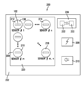
Ionizing radiation sensors 102 may be arranged into sensor arrays 204 (FIG. 2)
comprising one or more radiation sensors 102 and mounted on a printed circuit
board (PCB),
for example, as described below.
FIG. 1 illustrates a first sensor 104 encapsulated, for example, in a filter
material such
as a specific radiation attenuating material 108 or a "filtration bubble" 110
having, for
REPLACEMENT SI IEET
CA 02872729 2014-11-27
WO 2013/179273
PCT/1B2013/054517
27
example, a prescribed thickness. Up to "n" sensors 106 may be manufactured and
encapsulated in up to "n" different respective filtration bubbles 112, where
each filtration
bubble can consist of a similar or different materials or similar or different
material
thicknesses. In this example, filtration bubble 108 corresponds to sensor 106
such that sensor
106 is surrounded or encapsulated by filtration bubble 108. In some preferred
embodiments,
the filtration bubble may comprise a spherical geometry. Materials of the
filtration bubble
may include thin metallic layers including, for example, copper, tin,
aluminum, tungsten, etc.
The filtration bubble will characteristically be comprised of radiation
attenuating material(s)
capable of filtering out, for example, alpha particles and beta radiation.
Filter material such
as specific radiation attenuating material 108 or a "filtration bubble"
provides an optimal
angular response wherein the response of the sensor is independent of the
angle of incidence
of the radiation (or other measured quantity), i.e., the output of sensor 106
is the same (or
"flat") at all angles.
Additional aspects of the disclosed invention provide the use of MEMS and
nanotechnology sensors to simultaneously detect motion, global position,
radiation exposure,
and a process, such as the use of a software algorithm, to correlate radiation
exposure levels
over time with motion of the detector and with the global position of the
detector.
Accordingly, features of disclosed embodiments enable, at least, the following
advantages:
(1) providing the correlation of radiation exposure levels with time, motion
and global
position of the detector to provide unique and valuable information on how the
exposure
occurred; (2) allowing the global position to detect either via an on-board
GPS sensor or by a
connected external electrical device, such as a mobile smart device (e.g.,
smartphone), with a
built-in GPS sensor or by estimation from a mesh of networked devices; (3)
providing
enablement such that the time, motion and global position can be optionally
recorded when
the detected exposure exceeds a threshold level.
Hardware components of the disclosed invention are further illustrated in FIG.
2
wherein modular sensors are integrated on a single chip or electronic board
202 (e.g., PCB)
thus forming an integrated sensor module 200. Integrated sensor module 200
collects
radiation data and is configured to ultimately transmit the data to a remote
location such as a
wireless base station or other wireless communications device. The integrated
sensor module
200 is designed to be an independent sensor system that can be incorporated
into many
different form factor devices. The small size and self-contained nature of the
integrated
CA 02872729 2014-11-27
WO 2013/179273
PCT/1B2013/054517
28
sensor module 200 to be integrated into a wide range of devices such as a
badge, nametag,
key chain, bracelet, wrist watch, portable electronic device, MP3 Player,
pager, cell phone,
smartphone, laptop, tablet, glasses, article of clothing, wallet, purse or
jewelry.
The primary sensor 220 can either be a single sensor, a linear array of
sensors, or a
matrix of sensors to form the primary or modular sensor array 204, for example
employed
from the sensor array 100 of FIG. 1. Thus the modular sensor array 204 may
utilize only a
first sensor # 1 (212). Alternatively, modular sensor array 204 may comprise n
number of
rows such as from first sensor # 1 (212) to sensor # n (214). Alternatively
and/or in addition,
modular sensor array 204 may include m number of columns such as from first
sensor # 1
(212) to sensor # m (216). Thus, having n number of rows and m number of
columns,
modular sensor array 204 would extend from first sensor # 1 (212) to sensor #
m, n (218).
While ionizing radiation sensors 102 encapsulated within "filtration bubbles"
108 are
shown for illustrative purposes, those skilled in the art will readily
appreciate that the
modular sensor array 220 may consist of other suitable types of sensors (e.g.,
for non-
ionizing radiation, hazardous chemicals, or other biochemical substances).
Alternative
embodiments of the disclosed invention may also include chemical or other
sensors in
addition and/or as an alternative to ionizing radiation sensor 102. The
present invention
describes an integrated modular sensor 200 that provides unique information
about the
location and the motion of the sensor when a measurement is obtained. The
modular nature
of the described platform and device enables the use of other individual
sensors or as variable
combination of sensors chosen to meet the needs of potential end users. The
modularity is
achieved by developing the measurement devices as interchangeable modules that
can be
coupled to a central processing unit (CPU) that handles the collection of
time, motion,
position and temperature and the communication.
The primary sensor array 220 may be integrated with a motion and global
position
sensor package The motion and global position sensor package 206 will consist
of a single 3-
axis MEMS based accelerometer 222 that will determine if a primary data
exposure occurs
while the device is stationary or in motion as measured on a continual basis.
A primary data
exposure is a radiological event recorded by the primary sensor array 220. The
motion and
global position sensor package 206 will consist of a global position radio 223
that will
determine its position by either the on-board GPS radio 223 and/or by a
connected wireless-
enabled mobile device (e.g., smart phone or tablet with GPS sensing
capability, etc.) or by
CA 02872729 2014-11-27
WO 2013/179273
PCT/1B2013/054517
29
estimation through a mesh of networked devices. To minimize power consumption
of the
primary power source the device will preferentially determine location through
GPS sensors
with the lowest power means available to it. First by the connected wireless-
enabled mobile
device with GPS capability, second by onboard GPS sensor and third by
estimation through a
mesh of networked devices.
A wireless system on a chip (SOC) module 208 is configured to integrated
sensor
module 200. The wireless SOC module 208 is an integrated package consisting of
a central
processing unit and the wireless transceiver. Combining the wireless
transceiver into the
CPU chip in a SOC configuration allows a reduction in footprint and energy
consumption.
The wireless system on a chip (SOC) module 208 permits wireless transmission
from
integrated sensor module 200, for example, to a wireless receiver of another
electronic device
for electronic communication purpose(s). Such communications ability
facilitates efforts, for
example, in determining whether integrated sensor module 200 is within range
of the
aforementioned electronic device as further discussed below.
The present invention uses energy harvesting through micro mechanical systems
(MEMS) and photovoltaic systems to recharge the internal battery and extend
the powered
lifetime of the integrated sensor module 200. Embodiments of the disclosed
invention also
extend previous work using the MEMS devices of the integrated sensor module
200 to
convert resonant and vibrational mechanical motion into electrical energy and
photovoltaic
cells to convert ambient lighting into electrical energy. The present
invention uses MEMS to
convert the random mechanical energy of human motion into electrical energy,
and
photovoltaics to convert ambient light into electrical energy, both of which
can be stored in a
battery on the device and later used to power the above-described sensors of
the integrated
sensor module 200. MEMS based energy harvesting can be accomplished with
piezoelectric,
electrostatic or magneto-static devices. Piezoelectric energy harvesters
convert mechanical
strain of vibration in electrical energy. Electrostatic energy harvesters
collect energy from
the changing capacitance of vibrating separation of charged parallel plate
capacitors.
Magneto-static energy harvesters collect energy through the motion of a magnet
near an
electric coil, such that the changing magnetic field of the moving magnet
induces current
flow in the electric coil. Photovoltaic energy harvesters are based on solar
cells that convert
solar or ambient indoor light into electric current. The power harvester 210
will consist of
one or more energy harvesting devices. A power harvester 210 is incorporated
into the
CA 02872729 2014-11-27
WO 2013/179273
PCT/1B2013/054517
integrated sensor module 200 and connected to the battery. Power harvester 210
collects
energy via motion and/or movement of the integrated sensor module 200 and the
ambient
light to recharge the battery that supplies power to electronic board 202.
Thus, the present
invention will actively consume power as it operates and actively communicates
to external
5 wireless enabled devices. Power harvester 210 leverages existing work
within the MEMS
devices to convert periodic (resonant) vibrational mechanical motion into
electrical energy to
extend the battery that powers the runtime of the radiation measurement sensor
capability of
the integrated sensor module 200.
Through extensive historical data on the dose levels of personal monitoring
radiation
10 detectors it has been determined that 95% of users receive normal
occupational level doses.
By optionally collecting motion and position only when the detected exposure
exceeds a
preset threshold. The power consumption of the device can be greatly reduced.
The
combination of primary exposure data, time, motion and location creates a
unique data set
which may provide information about the location of radiation fields and the
motion of the
15 users through those fields.
Embodiments of the disclosed invention enable the use of ultra-low-power
wireless
transmission to transmit measured sensor readings from the sensor device 202
to a wireless-
enabled mobile device (e.g., a smartphone or tablet device, etc.), and the
transmission of this
information over a wired or wireless data network to an Internet-based server.
20 The uniquely configured electronic modular configuration of the
disclosed invention
provides several advantages. The filter material is machine pressed into a
spherical shape,
and the resulting "filtration bubble" 110 is mechanically pressed into the
circuit board
containing the ionizing radiation sensor elements 102. Disclosed embodiments
of the
invention will enact a unique software algorithm (as detailed below) to enable
the
25 discrimination between different types of ionizing radiation and
different radiation energies.
This enables a unique customization of the energy discrimination filtration
scheme to
improve the accuracy and energy resolution of ionizing radiation measurements
using a
passive radiation detector.
Radiation attenuating materials 108 are used to modify the response of non-
tissue
30 equivalent sensors to allow varying responses to a wide range of
radiation qualities. The
modified response can then be used by an algorithm to derive the tissue
equivalent dose.
Currently macro-filters utilized in convention sensor devices have several
shortcomings that
CA 02872729 2014-11-27
WO 2013/179273
PCT/1B2013/054517
31
limit the effectiveness of algorithms by introducing uncontrolled variances.
The use of
MEMS and nanotechnology manufacturing process to encapsulate the radiation
sensors with
"filtration bubble" 110 provides several advantages over the traditional macro-
filters that will
help eliminate the uncontrolled variances. The use of precise MEMS and
nanotechnology
manufacturing processes allows for the elimination of macro scale variances in
the separation
of the filter, thickness of the filter and location of the filter. The
filtration bubble 110 will
eliminate macro scale issues with angular dependence of the filtration. The
filtration bubble
110 will also provide a protective layer over the sensitive and possibly
fragile sensor 102.
The use of multiple attenuating materials 108 around multiple sensors 102 with
the use of a
software algorithm will allow increased levels of fine discrimination between
types of
ionizing radiation and radiation energy.
Additional advantages of the described embodiments of the present invention
utilize
MEMS and nanotechnology sensors to simultaneously detect radiation and other
exposure,
temperature, time, motion and global position, in combination with an employed
software
algorithm to correlate exposure levels. Detection occurs with the time, motion
and global
position of the integrated sensor module 200 wherein the chip 200 provides
unique and
valuable information on how the exposure occurred. The use of modular exposure
sensors
enables the detection and analysis of exposure to a wide range of phenomena
including, for
example, radiological, chemical, biological and electromagnetic sources of
exposure. The
use of time, motion and position further enables the determination of whether
the integrated
sensor module 200 was moving during an exposure event (e.g., static versus
dynamic
exposures), and when and where the exposure occurred. The present invention
replaces the
computationally intensive and time-consuming post-processing and analysis that
is currently
used by convention sensor devices to determine static versus dynamic
exposures. The
present invention also provides new time, position and other information that
can may be
used to accurately characterize the source and nature of the exposure. This
capability may be
particularly important/useful in occupational dosimetry. The inclusion of a
temperature
sensor is disclosed embodiments enables correction of measurements for
temperature-based
variance.
Furthermore, the present invention expands the capabilities and application of
traditional, standalone dosimeters by allowing collected data to be
transmitted to a central
location for processing and redistribution as shown in FIG. 3. FIG. 3
illustrates a remote
CA 02872729 2014-11-27
WO 2013/179273
PCT/1B2013/054517
32
sensor network 300 according to an exemplary embodiment of the invention.
Integrated
sensor module 200 is integrated into a dosimetry badge 310. Dosimetry badge
310 is
illustrated as a package, for example, including the disclosed electronics
packaging including
integrated sensor module 200, batteries and a cover of the present invention.
Integrated
sensor module 200 collects radiation data and ultimately transmits the data to
a remote
location such as a wireless base station or other wireless communications
device such as
mobile communications device 308. A remote sensor chip of integrated sensor
module 200
may be utilized to transmit the data. In this case, the data may be
transmitted via an
unspecified wireless transmission communication protocol 312 such as
Bluetooth0, ZigBee,
ANT, or other standard Wi-Fi protocol, etc.
Examples of mobile communication device 308 may include, for example, a smart
phone, tablet or a mobile hot-spot, or it might be a non-mobile network device
such as a
dedicated base station. Mobile communication device 308 may be configured to
include a
wireless transmitter and receiver 316, data network interface 318, and GPS
320. Wireless
system on a chip (SOC) module 208 of integrated sensor module 200 is
configured to
communicate with wireless transmitter and receiver 316. The wireless
transmitter and
receiver may be a low powered wireless network interface for the mobile
communication
device 308. The network interface allows the mobile communication device 308
to
communicate with the integrated modular wireless sensor chip 200 to download
collected
data. The aforementioned communication facilitates the determination of
whether mobile
communication device 308 is in range of integrated sensor module 200.
Mobile communication device 308 may also be configured to include a data
network
interface 318. The data network interface 318 allows mobile communication
device 308 to
communicate to another wide area wireless network 306 such as via data network
transmission communication protocol 314. Examples of data network transmission
communication protocol 314 may include Wifi, GSM/EDGE, CDMA, UTMS/HSPA+, LTE
or other high speed wireless data communication network. Thus, in an exemplary
embodiment, Bluetooth0 may be employed to communicate between the dosimetry
badge
310 and mobile communication device 308 (such as via wireless transmission
communication
protocol 312), and the use of LTE to communicate between mobile communication
device
308 and wireless network 306 (such as via data network transmission
communication
protocol 314) of a remote facility such as a hospital or laboratory. In this
example, the local
CA 02872729 2014-11-27
WO 2013/179273
PCT/1B2013/054517
33
network may be represented by wireless network 306 and the public network may
be
indicated by as public data network 302. By communicating, for example, over
the public
data network 302, the aforementioned remote facility, such as a hospital or
laboratory, may
reach, access and/or process information deposited on distributed data server
804.
GPS 320 enables mobile communication device 308 to determine the position of
the
radiological event. The GPS 320 radio in the mobile communication device 308
provides an
alternative means of the determining the position of the integrated sensor
module 200. If the
integrated sensor module 200 has been paired with a mobile communication
device 308, it
will preferentially use GPS sensor 320 to determine location to minimize its
own power
consumption.
Wireless network 306 is configured to communicate with the public data network
(e.g., the Internet) 302. A remote data server 304 is configured to
communicate with a public
data network (e.g., the Internet) 302.
With an electronic data transmission link formed between mobile communication
device 308 and remote data server 304, integrated sensor module 200 is capable
of
transmitting measured data such as to an ultra-low-power wireless-enabled
mobile
communication device 308 (e.g., a smart phone, tablet or other mobile or non-
mobile network
device) to leverage the mobile device's existing data or cellular network to
communicate
collected information to a central web server and, optionally, to use the
mobile
communication device GPS, or to process the collected data using the mobile
communication
device CPU. Currently, standalone sensor devices have limited power capacity
that must be
conserved as much as possible in order to extend battery life. Ultra-low-power
wireless
communication minimizes the power consumption of device for regular updates.
Furthermore, typical data or cellular communication antennas can consume
significant power,
so utilizing an external mobile communication device also limits the
complexity of radiation
sensor.
Thus, the use of ultra-low-power wireless transmission capability of the
present
invention allows transmission of measured sensor readings from integrated
sensor module
200 to a wireless-enabled mobile device 308 (e.g., a smartphone or tablet
device, etc.), and
the transmission of this information over a wireless data network 306 to an
Internet-based
server 302. This enables the analysis and reporting of measured doses for
individual
detectors employing integrated sensor module 200 without having to physically
send the
CA 02872729 2014-11-27
WO 2013/179273
PCT/1B2013/054517
34
detector itself to a central location for reading and analysis. The reduces
costs and valuable
time for receiving data and performing critical analysis. Embodiments of the
present
invention also allow for multiple systems to receive a plurality of measured
doses from a
plurality of detectors having integrated sensor module 200. The collection of
sensor data
from multiple systems enables the analysis and visualization and geographic-
based mapping
of exposure sources and related population-based trends over time. The
connection to the
Internet also enables the remote update and troubleshooting of the device.
Disclosed embodiments of the present invention may include mounting the
integrated
sensor module 200, for example, on multiple, low-cost, semi-autonomous
unmanned airborne
vehicles (UAV's) such as low-power RF helicopters. A flocking-algorithm may be
employed
to cause the "flock" of devices to track the position and distribution of
airborne radiation,
chemicals or other phenomena while remaining in the flock and where the
distribution of the
flock would correlate with the distribution of the airborne material being
tracked.
Thus, in select embodiments, the disclosed invention enables the integration
of the
integrated sensor module 200 into a mobile platform that may consist of
multiple semi-
autonomous UAV's to track the position and distribution of airborne materials
(radiation,
chemicals, biological agents, electromagnetic fields, etc.). The UAV-
integrated sensors may
utilize flocking algorithms to coordinate between multiple UAV's and track the
position and
distribution of airborne particles. Turning to FIG. 4 an exemplary autonomous
mobile sensor
(AMS) network 400 is illustrated. As shown in FIG. 4, the airborne (or
waterborne) particles
402 will tend to cluster and then distribute depending, for example, upon
prevailing weather
patterns. Autonomous mobile sensors (AMS) 404, 406 are shown tracking
respective
distributed target particles 408, 410. The flocking algorithm will update the
position of all
UAVs 404, 406 by using a Sensor Force, Fs, proportional to the measurement
from the sensor
array 204 on the UAV, and a Flocking Force, Ff, proportional to the distance
to nearby
UAV's, to continually optimize the positions of the UAV sensors 404, 406 and
to best track
the position of the target particles 408, 410. As a result, the distribution
of the flock will also
correlate with the distribution of the airborne material being tracked.
In another embodiment the disclosed invention may include mounting integrated
sensor module 200 on multiple, low-cost, semi-autonomous and unmanned water-
based
vehicles and tracking, for example, waterborne particles. Again, the use of
the previously
described flocking-algorithm may be employed to coordinate between multiple
unmanned
CA 02872729 2014-11-27
WO 2013/179273
PCT/1B2013/054517
water-based vehicles and to track the position and distribution of any water-
based radiation,
chemicals or other phenomena.
Advantages of the disclosed invention provide the first use of MEMS and
nanotechnology to create a passive integrating electronic ionizing radiation
detector with
5 active readout capability and with motion-sensing and position-sensing
capabilities and
wireless transmission of the sensor readings. Current active dosimeters
require continuous
power in order to measure dose. Additionally, current passive dosimeters do
not provide
immediate access to recorded dose measurements. Alternatively, the active
readout of a
passive radiation sensor disclosed by the present invention provides immediate
access to dose
10 information while preserving dose information in the event of power
loss. In addition, the
present invention describes an electronic platform for recording motion,
temperature and
position with modular environmental sensors for comprehensive personal and
environmental
monitoring.
An exemplary integrated sensor module logic flow 500 for integrated sensor
module
15 200 is represented in FIG. 5. A command 502 for reading the sensor is
executed. Command
502 includes pre-reading a high-sensitivity sensor 504 to determine if there
is a new threshold
dose 506 on the sensor.
In determining whether there is a new threshold dose 506 on the sensor, the
sensor is
enabled to continuously accumulate dose values. When a pre-read is performed
on the high-
20 sensitivity sensor, a cumulative value is generated. The previous dose
value is subtracted
from the cumulative value generated from the pre-read to generate a delta (A)
value. If the
delta (A) value above a prescribed dose threshold, then a trigger measurement
is taken in step
508. If the delta (A) value is not above the prescribed dose threshold then a
loopback
function is performed to take continuous measurements at a timed interval to
read the sensor
25 502. Described embodiments continuously loop back to pre-read high-
sensitivity sensor 504
until a delta (A) dose value is detected to be higher than the prescribed dose
threshold value.
Once a delta (A) dose value is detected to be higher than the prescribed dose
threshold value,
a trigger measurement 508 is enabled to simultaneously read a solid-state
sensor array 510
(also see FIG. 6) and read-out of the event data or point of exposure in time
512 (also see
30 FIG. 7).
One disclosed embodiment of the sensor readout logic flow diagram is
illustrated in
FIG. 6. The solid-state sensor array read-out 600 is the component of the
disclosed invention
CA 02872729 2014-11-27
WO 2013/179273
PCT/1B2013/054517
36
that reads the entire sensor array. A reading from the high sensitivity sensor
indicates that the
minimum incremental dose threshold has been reached. The high sensitivity
sensor is solely
intended to indicate when when the threshold dose has been exceeded. Once the
threshold
dose has been exceeded the full dose will be read. The full dose can be read
from a 1-D
array, a 2-D array Of a 3-D matrix. A 1-D array may just be a fOWT of sensors.
A 2-D array
may be a table of sensors or a matrix of sensors. A 3-D array would be if you
stack up
multiple 2-D arrays. We can have multiple ways of reading this out. We could
either read
each sensor individually 602, or we might read-out along an entire row or
column of sensors
604, or we might sum up the output from all of the sensors 606, or you could
readout a
custom configuration (e.g., four of the sensors in each quadrant if there was
an array of
multiple sensors (e.g., sixteen sensors). Hence, disclosed embodiments of the
described
invention provide multiple ways of reading a solid-state sensor array.
One disclosed embodiment of the sensor readout logic flow diagram is
illustrated in
FIG. 6. The solid-state sensor array read-out 600 is the component of the
disclosed invention
that reads the entire sensor array. In one example, the high sensitivity
sensor may be affixed
to a badge. In an event where the badge is exposed to ionizing radiation the
disclosed
invention can read out the full dose of exposure. Disclosed embodiments
provide the ability
to read individual, a whole array of sensors, and a custom configuration of
sensors.
Accordingly, for various configurations of sensors, the invention may generate
readings, for
example, for individual sensors 602 such as a one-dimensional array including,
for example,
a row of sensors. In addition to or alternatively, dimensional arrays of
sensors may be read
by disclosed embodiments to include, for example, a table of sensors or a
matrix of sensors.
Such embodiments of sensor configurations may include a two-dimensional array
of sensors
including, for example, one or more rows or one or more columns of sensors.
Disclosed
embodiments may also provide a three-dimensional array, for example, including
one or
more two-dimensional arrays stacked upon one another. Thus, disclosed
embodiments may
either read sensors individually 602, perform a two-dimensional read-out, for
example, along
an entire row or column of sensors 604, or perform a sum of all of the output
from all of the
sensors 606, or perform a readout for a custom configuration of sensors (e.g.,
four of the
sensors in each quadrant if there was an array of multiple sensors (e.g.,
sixteen sensors)).
Hence, disclosed embodiments of the described invention provide multiple ways
of reading a
solid-state sensor array.
CA 02872729 2014-11-27
WO 2013/179273
PCT/1B2013/054517
37
Disclosed embodiments provide electronic sensing circuitry to generate an
analog
measurement. The analog measurement is preferably converted to a digital
measure utilizing
standard analog to digital conversion circuitry 610. From the digital data,
the dose 612 is
calculated by implementing an algorithm of the disclosed invention for
calculating the dose
on a system on a chip (SOC) (e.g., via an arm processor). The calculated dose
value is then
recorded on a data record 614 which may essentially generate a log of all of
the readings on a
continuous basis.
In parallel with the solid-state sensor array read-out 600 of FIG. 6, the
disclosed
invention executes a read-out of the event data or point of exposure in time
512. The point of
exposure read-out logic flow 700 is illustrated in FIG. 7 and may be executed
via parallel
circuitry. An on-board MEMS accelerometer device 702 is read to determine if
the sensor is
in motion. Next, the position of the sensor is estimated 704. This may be
accomplished, for
example, by reading the GPS sensor on the integrated sensor module or by
communicating
with a mobile device (e.g., cell phone) in which the GPS function of the
mobile device is
utilized to determine the geospatial position. The GPS receiver of the mobile
device
determines position by precisely timing the signals sent by GPS satellites.
Each satellite
continually transmits messages that include the time the message was
transmitted and the
satellite position at the time of message transmission. The GPS receiver uses
the messages it
receives to determine the transit time of each message and computes the
distance to each
satellite using the speed of light. Each of these distances and satellites'
locations define a
sphere. The receiver is on the surface of each of these spheres when the
distances and the
satellites' locations are correct. These distances and satellites' locations
are used to compute
the location of the receiver using navigation equations. In another
embodiment, the position
may be estimated by triangulating the position such as from a known wireless
hub with which
the sensor is communicating. Wireless triangulation is the process of
determining a location
of a point by measuring signal strength between several nodes of the wireless
network. A
time stamp is generated 706 to record the time at which a measurement was
taken. This
measure correlates to the motion (e.g., point at which on-board MEMS
accelerometer device
is read 702) and position (e.g., the estimated position of the sensor 704) at
the time the sensor
was read. The time stamp readings 706 may then be exported or recorded to the
data log.
Thus, the exposure event is captured in the data record 708.
CA 02872729 2014-11-27
WO 2013/179273
PCT/1B2013/054517
38
Turning again to FIG. 5, the above description outlines the generation of a
dose value
510 and a point of exposure in time 512 in the log or recorded data records
614 and 708,
respectively, to generate a complete data record 514. The complete data record
514 is saved
or updated to the record log and the Send Timer is checked 516. The Send Timer
determines
when data should be uploaded to the base station 802 or mobile communication
device 308
based on a programmable Time To Send value. For example, if the dose exceeds a
prescribed threshold value or if the prescribed time has elapsed, then the
dose value is
transmitted and recorded 522. If the Time to Send value has not been reached,
then the
device will return to reading 520.
The wireless transmission is started 524 in order to initiate sending a signal
from the
sensor wireless transmitter 208 of the integrated sensor module 200, for
example, to wireless
receiver 316 of mobile communication device 308. The sensor's wireless
transmitter 208
looks for a handshake response from the wireless transmitter 316 of the mobile
communications device 308 to determine if the device is in range for further
communication.
Sensor wireless transmitter 208 of the integrated sensor module 200 can be
configured to
communicate with another electronic communications device, such as base
station 802, to
determine if it is within range of the electronic communications device. If a
receiver is
within range and a response is received, then the operation continues 528. If
a determination
is made that the sensor is not in range, then a determination of "no" is made
526 and the
operation returns to read the sensor 502 again. When a determination is made
that the sensor
is in range, a determination of "yes" is made 528, and the data record is
transmitted such that
the log is updated to show that the data record has been transmitted 530 and
to record that the
system has been updated. A continuous, never-ending number of readings may
occur or as
needed in the integrated sensor module logic flow 500.
FIG. 8 illustrates an exemplary embodiment of the disclosed invention in
communication with a wireless sensor base station configuration 800. One or
more
generalized data servers can be connected to a public data network, such as
the Internet, to
provide an event repository wherein all of the event data is stored in one or
more databases
accessible over the Internet, and wherein further data analysis can be
performed. The Internet
is sometimes referred to The Cloud, and access to data over The Cloud for
further analysis is
sometimes referred to as Cloud Computing.
CA 02872729 2014-11-27
WO 2013/179273
PCT/1B2013/054517
39
Dosimetry badge 310 is illustrated as a package containing, for example, the
disclosed
electronics packaging including integrated sensor module 200, batteries and a
cover of the
present invention. Using the algorithm (FIG. 6 and 7), the integrated sensor
module 200 is
configured to transmit data to a wireless communications device such as a
wireless sensor
base station 802. Dosimetry badge 310 may communicate with wireless sensor
base station
802 via an unspecified wireless transmission communication protocol including,
for example,
Bluetooth0, Bluetooth Low Energy (BLE), ZigBee, ANT, ANT+ or other standard
wireless
communications protocols.
Wireless sensor base station 802 includes a wireless transmitter and receiver
816.
Wireless system on a chip (SOC) module 208 of integrated sensor module 200
communicates
with wireless transmitter and receiver 816 to determine whether base station
802 is in range
of integrated sensor module 200 as discussed, for example, in step 532 of FIG.
5 above.
Wireless sensor base station 802 may also include a data network interface
818. Data
network interface 818 allows wireless sensor base station 802 to communicate
to another
wireless network such as via data network transmission communication protocol
314. Thus,
in an exemplary embodiment, Bluetooth0 Low Energy (BLE) may be employed to
communicate between the dosimetry badge 310 and wireless sensor base station
802 (such as
via wireless transmission communication protocol 312), and Wi-Fi may be
employed to
communicate between wireless sensor base station 802 and wireless network 306
(such as via
data network transmission communication protocol 314) of a remote facility
such as a
hospital or laboratory. In this example, the local network may be represented
by wireless
network 306 and the public network may be indicated by as public data network
302. By
communicating, for example, over the public data network 302, the
aforementioned remote
facility, such as a hospital or laboratory, may reach, access and/or process
information
deposited on distributed data server 804.
In an optional configuration, wireless sensor base station 802 may include
integrated
sensor module 200. This configuration enables wireless sensor base station 802
as an event
sensing device as well, acting, for example, as an environmental sensor.
As previously discussed, disclosed embodiments of the invention will employ a
unique software algorithm to enable the discrimination between different types
of ionizing
radiation and different radiation energies. This enables a unique
customization of the energy
discrimination filtration scheme to improve the accuracy and energy resolution
of ionizing
CA 02872729 2014-11-27
WO 2013/179273
PCT/1B2013/054517
radiation measurements using a passive radiation detector. Disclosed
embodiments provide
electronic sensing circuitry to generate an analog measurement. The analog
measurement is
preferably converted to a digital measure utilizing standard analog to digital
conversion
circuitry 610. From the digital data, the dose 612 is calculated by
implementing the
5 algorithm of the disclosed invention for calculating the dose on a system
on a chip (SOC)
(e.g., via an arm processor). Select embodiments may employ, for example, a
machine
readable medium having stored thereon sequences of instructions, which when
executed by
one or more processors, cause one or more electronic devices to perform a set
of operations
to perform the aforementioned algorithm. The calculated dose value is then
recorded on a
10 data record 614 which may essentially generate a log of all of the
readings on a continuous
basis.
Accordingly, an embodiment of the invention provides a numerically optimized
dose
calculation algorithm for accurate and reliable personal dosimetry. Disclosed
embodiments
provided a computational procedure to generate numerically optimized dose
calculation
15 algorithms for personal dosimeters using multiple dosimeter elements
(typically two-to-four
elements). Current embodiments provide a description of how methods of the
present
invention transforms dosimeter signals to operational quantities for personal
dose equivalents
such as Hp(10), Hp(3), and Hp(0.07). Some advantages of the computational
procedure of
the disclosed invention include the ability to automatically generate a
numerically optimized
20 algorithm, the absence of branching or empirical decision points, and
fast computation speed.
The accurate and reliable measurement of a personal dose equivalent is a key
component of radiation dosimetry programs. The personal dose equivalent is
typically
measured over a wide range of energies and from different radiation sources,
including, for
example, x-ray and gamma photons, beta particles and neutrons. In order to
accurately
25 estimate the dose from different radiation sources, some personal
dosimeters incorporate
multiple detector elements, each with varying types of radiation filtration
materials, and use a
dose calculation algorithm, to calculate the personal dose equivalent from a
numerical
combination of the responses from each detector element.
One approach to calculate the dose is to use a simple linear combination of
detector
30 element responses. Such approaches are straight-forward and easy to
implement, but may be
highly sensitive to noise and often do not reliably provide an accurate
estimate of the dose
under realistic conditions. Another approach is to use empirically-determined
branching and
CA 02872729 2014-11-27
WO 2013/179273
PCT/1B2013/054517
41
decision points. According to exemplary embodiments, this approach is
relatively easy to
implement, and improves performance under some conditions, but the empirical
decisions are
unique to specific conditions, and often subject to systematic biases.
Techniques for applying
both linear combination and branching methods to radiation dosimetry have been
developed,
for example, by N. Stanford (e.g., see N. Stanford, Whole Body Dose Algorithm
for the
Landauer InLight Next Generation Dosimeter, Algorithm Revision: Next Gen IEC;
Sept. 13,
2010 and N. Stanford, Whole Body Dose Algorithm for the Landauer InLight Next
Generation Dosimeter, Algorithm Revision: Next Gen NVLAP; Sept. 27, 2010).
The present invention provides MATRIX i.e., a computational procedure to
automatically generate a dose calculation algorithm that is numerically
optimized for a
particular dosimeter type (i.e., a particular combination of dosimeter
detector elements and
filters). In order to minimize systematic bias the disclosed embodiment, i.e.,
MATRIX
calculates a weighted average from representative data, such that no one
irradiation field,
detector or ratio of detector signals dominates the resultant dose. The
following describes the
computational procedure used to generate a numerically-optimized dose
calculation
algorithm for a personal dosimeter using a matrix of element responses
obtained from
measurements of that type of dosimeter.
Given a personal dosimeter consisting, for example, of multiple filtered
detector
elements, the detected signal from each detector element is called the element
response, and
the array of element responses from a given dosimeter is called the detector's
element
response pattern. For a given type of dosimeter, the matrix resulting from
multiple detector
element responses at different but known irradiations is called the element
response matrix.
The element response matrix is created by exposing a dosimeter to known
irradiations
at different angles and to mixtures of individual or multiple sources, and
then reading the
element responses from each detector element. The element response pattern
from an
unknown irradiated dosimeter is then compared to the patterns in the element
response
matrix, and a dose is calculated for each source in the response matrix. The
final reported
dose is the sum of all the individual source doses weighted by a Source
Probability Factor.
The Source Probability Factor is a measure of how closely the element response
pattern of
the unknown dosimeter matches the individual element response pattern of known
sources.
CA 02872729 2014-11-27
WO 2013/179273
PCT/1B2013/054517
42
The steps in the disclosed embodiment, i.e., MATRIX computational procedure
900
are summarized in Table 1 of FIG. 9, and each computational procedure is
described in the
corresponding sections below.
In step 902, the dosimeter element responses and the corresponding dosimeter
response matrix for that type of dosimeter are input, and then the converted
values are
calculated. For dosimeters employing optically simulated luminescence (OSL)
such as
LANDAUER's InLight dosimeters, the dosimeter element responses correspond to
the
photomultiplier counts from the InLight Reader. The converted values are
calculated from
the PMT counts as shown in Equation 1:
FAIT Catimtp,
011'4
raltt iloladfr_t..aLraclgr
The response matrix corresponding to the dosimeter type may be read from
computer
storage. In one disclosed example, e.g., for LANDAUER InLight dosimeters, the
response
matrix contains entries (variables) describing the source, the individual
element responses,
the deep dose equivalent (DDE) conversion factor, and the standard deviations
of the
responses.
The response matrix selection may be based on empirically derived rules. In
order to
achieve optimal performance in a certain application, the range of sources in
the response
matrix is restricted. This technique may cause a systematic error if radiation
conditions occur
outside the selected range. An implementation of the disclosed embodiment
using selection
cuts is described, for example, in Brahim Moreno, LDR-Europe Technical Report
on a
Hybrid MATRIX-Branching dose calculation algorithm, 2013.
Next a dose calculation may be performed. Given a set of measured converted
values,
the first step is to calculate G1-4 for each field in the response matrix.
Note that the values of
G for a given field indicate what the SDE would be if the given field matched
the actual
incident field to the dosimeter.
The expected value of the SDE for a given field could be taken as the simple
average
of G over the detector elements. This however would be insufficient due to the
fact that for
some incident radiation fields, several detectors may have signals with high
levels of
CA 02872729 2014-11-27
WO 2013/179273
PCT/1B2013/054517
43
uncertainty. This turns out to be the case with 85Kr 13-rays incident upon
detectors with
filtration over 0.1 g/cc in density thickness. Because of this field is weakly
penetrating, the
signals received from the filtered elements are too low relative to the noise
level to use them
to calculate dose.
A way to calculate dose using only detectors with a good signal is to weight
the signal
of each detector by a factor inversely proportional to the expected
uncertainty and then
perform a weighted average over the detectors. The first set is to define the
expected
uncertainty. Assume that each response matrix entry is determined from data
for which the
counting statistics were negligible (high dose). This error is a combination
of the
uncertainties due to the irradiation, reading, handling, and material
variability. This
combined error is computed as the standard deviation of the data used to
generate the
response matrix, it is symbolized by 6.
The expected value of the SDE for field j is given by The
total uncertainty for the
ith detector element and jth radiation field is by symbolized by gq.
;
(2)
341.-
A goodness of fit statistic for a single radiation field, j, is given in
Equation 3.
4.
I
The weighting factor for field j is given in Equation 4.
(-4)
¨1)2
CA 02872729 2014-11-27
WO 2013/179273
PCT/1B2013/054517
44
Now that a weighting factor has been assigned to each field in the response
matrix,
the reported SDE value, Grep, is calculated. This is done by taking the
weighted sum of the
expected values for each radiation field GI, over the entire response matrix.
This is given in
Equation 5, where the sum is performed over a response matrix of N
F,õ
z.
W,
Et =
The quantification of similarity between the response pattern of a measured
set of
converted values and the fields in the response matrix can be derived using
any optimization
technique. Equations 3-4 are based on the x2 minimization. The source specific
statistic and
weighting factor are an empirical measure of how well the pattern of a set of
measured
converted values matches the patterns found in the response matrix.
In step 904, a check for error conditions is performed. In this step, common
error
conditions are checked and, if detected, the appropriate error conditions are
set. The dose is
not reported if a serious error condition is detected.
In step 906, dose values are calculated for each source in the response
matrix. In this
step, a weighted value for Hp(0.07) and Hp(10) are calculated for each element
to form the
response pattern for this dosimeter. Then a goodness of fit statistic is
calculated, and then a
source weighting factor is determined.
In step 908, disclosed embodiments calculate the total reportable doses. In
this step,
the weighted values for Hp(0.07) and Hp(10) for each element are summed, then
the source
weighting factors for each element are summed. The reportable Hp(0.07) and
Hp(10) doses
are calculated.
In step 910, an estimate of the most likely source of radiation is performed.
In this
step, the probable contribution of each source in the response matrix is
estimated. In the
currently disclosed algorithm, the probable contribution of photons and beta
particles is
estimated.
CA 02872729 2014-11-27
WO 2013/179273
PCT/1B2013/054517
In step 912, the final (net) dose values are calculated. In this step, the net
dose is
calculated by subtracting a control dose from the previously calculated dose.
Only net doses
greater than 1.0 mrem are reported.
In step 914, the net dose values are outputted, e.g., from memory to storage
device.
5 In this
step, the net dose is assigned to a specific dosimeter using the unique
identification
value stored in the dosimeter information database. The calculated Net Dose in
computer
memory is stored in the database (or exported to an external data file if
needed. The results
can be formatted to allow the generation of dose-of-record customer dose
reports as required
by local, national or international regulations.
10 A
flowchart 1000 of the disclosed computational procedure for employing an
algorithm to generate numerically optimized radiation dose calculations for
personal
dosimeters is illustrated in FIG. 10. Information/data from the dosimeter
readout 1004,
background radiation dose 1006 and response matric 1008 may be read and
inputted from a
computer storage 1002 such as a computer disk and stored to a machine readable
medium
15 such as
memory 1010. The machine readable medium or memory 1010 may have stored
thereon sequences of instructions, which when executed, for example, by one or
more
processors, may cause one or more electronic devices to perform a set of
operations to
perform the disclosed computer algorithm. The disclosed computer algorithm
processes the
raw data (e.g., dosimeter readout 1004, background dose 1006, and response
matrix 1008)
20 and
transforms it to useful information which may be further written to a computer
storage
1016 such as a computer disk where the information may be configured to be
displayed as
needed.
After the raw data is received to memory 1010, disclosed embodiments check for
error conditions 1012. Common error conditions are checked and, if detected,
the error may
25 be
flagged 1014 and all errors may be tracked/tabulated on computer storage 1016.
If there is
no error 1018, the raw data is processed by the disclosed computer algorithm
1020.
Computer algorithm 1020 begins by applying a mathematical algorithm using
prescribed
numerical procedures to optimize the response matrix. This may include
calculating the
expected source dose with a data-fitting procedure. The inputs are the
converted values and
30 source
responses. The response matrix weighting factor may be calculated using a
goodness-
of-fit statistic. The weighting factors tell you how much each source
contributes to the final
dose. An optimization technique may be selected based upon prescribed
performance
CA 02872729 2014-11-27
WO 2013/179273
PCT/1B2013/054517
46
criteria. The Dose contribution may be calculated from the product of the
weighting factor,
expected source does, and dose conversion factor for personal dose equivalent
(e.g., Hp(10
mm), Hp (0.07 mm), and Hp (3 mm)).
Once the optimal fit is found/determined, the reportable doses are calculated
1022 by
summing the dose contributions for each source output dose. Radiation quality
is assessed
1024 by performing a sum over the weighting factors multiplied by the source
energy and
particle identification. The radiation quality may be written to computer
storage 1028 such as
to computer disk 1016. The net dose is calculated by subtracting the
reportable doses and
background dose. The net doses may be written to computer storage 1030 such as
to
computer disk 1016.
The devices and subsystems of the disclosed exemplary embodiments can store
information relating to various processes described herein. This information
can be stored in
one or more memories, such as a hard disk, optical disk, magneto-optical disk,
RAM, and the
like, of the devices and subsystems of the disclosed exemplary embodiments.
One or more
databases of the devices and subsystems of the disclosed exemplary embodiments
can store
the information used to implement the exemplary embodiments of the present
invention. The
databases can be organized using data structures (e.g., records, tables,
arrays, fields, graphs,
trees, lists, and the like) included in one or more memories or storage
devices listed herein.
The processes described with respect to the disclosed exemplary embodiments
can include
appropriate data structures for storing data collected and/or generated by the
processes of the
devices and subsystems of the disclosed exemplary embodiments in one or more
databases
thereof.
All or a portion of the devices and subsystems of the disclosed exemplary
embodiments can be conveniently implemented using one or more general purpose
computer
systems, microprocessors, digital signal processors, micro-controllers, and
the like,
programmed according to the teachings of the exemplary embodiments of the
present
invention, as will be appreciated by those skilled in the computer and
software arts.
Appropriate software can be readily prepared by programmers of ordinary skill
based on the
teachings of the exemplary embodiments, as will be appreciated by those
skilled in the
software art. In addition, the devices and subsystems of the disclosed
exemplary
embodiments can be implemented by the preparation of application-specific
integrated
circuits or by interconnecting an appropriate network of conventional
component circuits, as
CA 02872729 2014-11-27
WO 2013/179273
PCT/1B2013/054517
47
will be appreciated by those skilled in the electrical art(s). Thus, the
exemplary embodiments
are not limited to any specific combination of hardware circuitry and/or
software.
Stored on any one or on a combination of computer readable media, the
exemplary
embodiments of the present invention can include software for controlling the
devices and
subsystems of the disclosed exemplary embodiments, for driving the devices and
subsystems
of the disclosed exemplary embodiments, for enabling the devices and
subsystems of the
disclosed exemplary embodiments to interact with a human user, and the like.
Such software
can include, but is not limited to, device drivers, firmware, operating
systems, development
tools, applications software, and the like. Such computer readable media
further can include
the computer program product of an embodiment of the present invention for
performing all
or a portion (if processing is distributed) of the processing performed in
implementing the
disclosed exemplary embodiments. Computer code devices of the exemplary
embodiments
of the present invention can include any suitable interpretable or executable
code mechanism,
including but not limited to scripts, interpretable programs, dynamic link
libraries (DLLs),
Java classes and applets, complete executable programs, Common Object Request
Broker
Architecture (CORBA) objects, and the like. Moreover, parts of the processing
of the
exemplary embodiments of the present invention can be distributed for better
performance,
reliability, cost, and the like.
As stated above, the devices and subsystems of the disclosed exemplary
embodiments
can include computer readable medium or memories for holding instructions
programmed
according to the teachings of the present invention and for holding data
structures, tables,
records, and/or other data described herein. Computer readable medium can
include any
suitable medium that participates in providing instructions to a processor for
execution. Such
a medium can take many forms, including but not limited to, non-volatile
media, volatile
media, transmission media, and the like. Non-volatile media can include, for
example,
optical or magnetic disks, magneto-optical disks, and the like. Volatile media
can include
dynamic memories, and the like. Transmission media can include coaxial cables,
copper
wire, fiber optics, and the like. Transmission media also can take the form of
acoustic,
optical, electromagnetic waves, and the like, such as those generated during
radio frequency
(RF) communications, infrared (IR) data communications, and the like. Common
forms of
computer-readable media can include, for example, a floppy disk, a flexible
disk, hard disk,
magnetic tape, any other suitable magnetic medium, a CD-ROM, CDRW, DVD, any
other
CA 02872729 2015-06-25
48
suitable optical medium, punch cards, paper tape, optical mark sheets, any
other suitable
physical medium with patterns of holes or other optically recognizable
indicia, a RAM, a
PROM, an EPROM, a FLASH-EPROM, any other suitable memory chip or cartridge, a
carrier wave, or any other suitable medium from which a computer can read.
REPLACEMENT SHEET