Note: Descriptions are shown in the official language in which they were submitted.
CA 02873525 2014-11-13
WO 2013/171488
PCT/GB2013/051253
1
COMPACT HIGH VOLTAGE RF GENERATOR
USING A SELF-RESONANT INDUCTOR
BACKGROUND OF THE INVENTION
[0001] Field of the Invention -- The present
invention relates generally to radio frequency (RF)
generators and more particularly to RF generator
circuits using an inductor.
[0002] RF
generators produce high frequency signals
useful for many applications, for example, for use in
ion mobility spectrometers (IMS) and field asymmetric
ion mobility spectrometers (FAIMS) or differential
mobility spectrometers (DMS). In a
spectrometer,
molecules in a sample of air are ionized and are
admitted into a drive region of a cell. The ionized
molecules drift to the opposite end of the cell at a
speed dependent on the size of the ion to a collector,
which causes a current pulse in the collector. The
current into the collector is converted to a voltage
and amplified. By measuring the time of flight along
the cell it is possible to identify the ion.
[0003] The subject matter discussed in this
background of the invention section should not be
assumed to be prior art merely as a result of its
mention in the background of the invention section.
Similarly, a problem mentioned in the background of
the invention section or associated with the subject
matter of the background of the invention section
should not be assumed to have been previously
recognized in the prior art. The subject
matter in
the background of the invention section merely
CA 02873525 2014-11-13
WO 2013/171488
PCT/GB2013/051253
2
represents different approaches, which in and of
themselves may also be inventions.
SUMMARY OF THE INVENTION
[0004] RF generator
circuits including a series
breesounsaendt ctiorcpuriotduadree daeshcriigbhedl.oadIn voltage at
oadtimeanth, high
RF generator circuit includes an active device driving
the series resonant circuit that includes a bifilar
toroidal dual inductor. The RF generator circuits may
frequency to drive a capacitive load.
[0005] In one
aspect, an embodiment of a circuit
including a dual inductor is provided. The dual
inductor includes a toroidal core. The circuit
includes a winding on the toroidal core. The winding
includes an input and an output. The circuit
also
includes another winding on the toroidal core. The
another winding includes an input and an output. The
circuit also includes a capacitor electrically coupled
to the input of the one winding in parallel with the
one winding. The circuit
also includes another
capacitor electrically coupled to the input of the
another winding in parallel with the another winding.
The outputs of the windings are configured to
electrically couple to a capacitive load.
[0006] In another
aspect, an embodiment of an RF
generator circuit including a power supply, an active
device configured to output a signal, a dual inductor
including a pair of windings wound on a toroidal core,
and a capacitor is provided. The capacitor
is
electrically coupled with one of the windings of the
dual inductor. The power supply and the active device
CA 02873525 2014-11-13
WO 2013/171488
PCT/GB2013/051253
3
are electrically coupled with the capacitor and the
one of the windings of the dual inductor. The dual
inductor is configured to provide a voltage step up of
the signal of the active device.
[0007] Another embodiment
of the invention relates
to a method of generating a signal. The method
includes providing a drive signal to an active device.
The method also includes providing a power supply.
The method also includes providing a circuit including
a bifilar toroidal dual inductor and a capacitor
electrically coupled in parallel with at least one of
the windings of the bifilar toroidal dual inductor.
The active device and the power supply are
electrically coupled to the circuit. The method also
includes driving a capacitive load electrically
coupled to the circuit in series with the bifilar
toroidal dual inductor.
[0008] This
Summary of the Invention is provided to
introduce a selection of concepts in a simplified form
that are further described below in the Detailed
Description. This
Summary of the Invention is not
intended to identify key features or essential
features of the claimed subject matter, nor is it
intended to be used to limit the scope of the claimed
subject matter.
CA028735252014-11-13
WO 2013/171488
PCT/GB2013/051253
4
DESCRIPTION OF THE DRAWINGS
[0009] The
detailed description is described with
reference to the accompanying figures. In the
figures, the left-most digit(s) of a reference number
identify the figure in which the reference number
first appears. The use of the same reference number
in different instances in the description and the
figures may indicate similar or identical items.
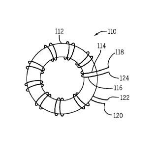
[0010] FIG. 1 is a
schematic illustration of a
self-resonant dual inductor in accordance with an
embodiment of this disclosure;
[0011] FIG. 2 is a
schematic illustration of a
self-resonant dual inductor in a series resonant
circuit in accordance with an embodiment of this
disclosure;
[0012] FIG. 3 is a
schematic illustration of an
embodiment of an RF generator circuit including an
embodiment of a series resonant circuit with a self-
resonant dual inductor in accordance with an
embodiment of this disclosure;
[0013] FIG. 4 is a schematic illustration of
another embodiment of an RF generator circuit
including an embodiment of a series resonant circuit
with a self-resonant dual inductor in accordance with
an embodiment of this disclosure; and
[0014] FIG. 5 is a schematic illustration of
another embodiment of an RF generator circuit
including an embodiment of a series resonant circuit
with a self-resonant dual inductor in accordance with
an embodiment of this disclosure.
CA 02873525 2014-11-13
WO 2013/171488
PCT/GB2013/051253
DETAILED DESCRIPTION OF AN EXEMPLARY EMBODIMENT
[0015] Prior to
turning to the figures, in one
embodiment, an RF generator using an active device to
drive a series resonant circuit including a self-
5 resonant dual inductor is provided. In one
embodiment, the RF generator produces two antiphase
outputs at a higher voltage than a supply voltage of
the RF generator at a frequency of at least one
Megahertz (MHz). Such outputs may be used to drive a
capacitive load. An embodiment of a self-resonant
dual inductor is first described.
[0016] A self-
resonant dual inductor, illustrated
as a bifilar toroidal dual inductor 110 in FIG. 1 is
provided. The bifilar
toroidal dual inductor 110
includes a generally toroid-shaped core 112. In one
embodiment, the core 112 is a low permeability
magnetic core (e.g., formed from iron powder, ferrite,
or other suitable materials).
Particularly, for
example, in one embodiment the core 112 is formed from
T 80-6 iron powder.
[0017] The core
112 is wrapped with a pair of
windings 114 and 116. The
windings 114 and 116 are
insulated conductors. In one embodiment the material
insulating the conductors has low RF loss and high
breakdown voltage characteristics, such as, for
example, polytetrafluoroethylene (PTFE), or other
suitable materials. The
windings 114 and 116 are
coupled. The winding 114 provides an input 118 and an
output 120. Likewise,
the winding 116 provides an
input 122 and an output 124. Embodiments of a bifilar
toroidal dual inductor 110 provide a low radiated
magnetic field and, in some embodiments, a smaller
CA 02873525 2014-11-13
WO 2013/171488
PCT/GB2013/051253
6
size than an air-gap inductor. Additionally, in some
embodiments, the bifilar winding configuration
provides close coupling between windings and simple
construction. In one embodiment, the core 112 is not
a split core (i.e., does not have an air gap).
[0018] Such a
bifilar toroidal dual inductor 110
may be used in various circuits. FIG. 2 illustrates a
series resonant circuit 248 including a self-resonant
dual inductor, such as the bifilar toroidal dual
inductor 210. One input 203 to the
circuit 248 is
electrically coupled with a capacitor 240 and the
input 218 of the winding 214 of the bifilar toroidal
dual inductor 210. The
capacitor 240 is also
electrically coupled to ground. Another input 205 to
the circuit 248 is electrically coupled with another
capacitor 242 and the input 222 of the winding 216 of
the bifilar toroidal dual inductor 210. The capacitor
242 is also electrically coupled to ground. The
output 220 of the winding 214 is electrically coupled
to a capacitor 244. The capacitor 244 is
also
electrically coupled to ground. The output 224 of the
winding 216 is electrically coupled to a capacitor
246. The
capacitor 246 is also electrically coupled
to ground.
[0019] Two inputs, with
phases shifted from one
another, may be applied to the inputs 203 and 205 of
the series resonant circuit 248. The inductors of the
bifilar toroidal dual inductor 210 are coupled, and
the bifilar toroidal dual inductor 210 is a self-
resonant dual inductor that produces two antiphase
outputs. As illustrated in FIGS. 1 and 2, the bifilar
toroidal inductor 310 is configured such that current
CA 02873525 2014-11-13
WO 2013/171488
PCT/GB2013/051253
7
flow through the windings 214 and 216 is in opposite
directions. The inter-
winding capacitance of the
bifilar toroidal dual inductor 210 provides series
resonance.
[0020] FIG. 3 is a
schematic illustration of an
embodiment an RF generator circuit 325 including a
self-resonant dual inductor, illustrated as a bifilar
toroidal dual inductor 310. A power
supply,
illustrated as a low voltage DC power supply 326 in
FIG. 3, is provided. The DC power supply
326 is
electrically coupled with a transformer 328. The
transformer 328 has two outputs 330 and 332. The
transformer 328 produces two outputs that are out of
phase with one another at the outputs 330 and 332.
[0021] An active device, illustrated as a
transistor 334, is also provided. While the
transistor 334 is illustrated as an NMOS field effect
transistor in FIG. 3, in other embodiments other
suitable transistors (e.g., PMOS FET's, JFET's, BJT's,
etc.) are used. Additionally, any
other suitable
active device may be used. The
transistor 334
receives a drive signal at an input 336. The source
of the transistor 334 is electrically coupled to
ground.
[0022] The output 338 of the
transistor 334, in the
illustrated embodiment the drain of the transistor
334, and the first output 330 of the transformer 328
are electrically coupled with the input 318 of the
winding 314 of the bifilar toroidal dual inductor 310
and to the first capacitor 340. The first capacitor
340 is electrically coupled in parallel with the
CA 02873525 2014-11-13
WO 2013/171488
PCT/GB2013/051253
8
winding 314 and is also electrically coupled to
ground.
[0023] The second
output 332 of the transformer 328
is electrically coupled with the second capacitor 342
and the input 322 of the winding 316 of the bilfilar
toroidal inductor 310. The second
capacitor 342 is
electrically coupled in parallel with the winding 316
and is also electrically coupled to ground.
[0024] The
inductors of the bifilar toroidal dual
inductor 310 are closely coupled. The bifilar
toroidal dual inductor 310 is a self-resonant dual
inductor that produces two antiphase outputs. As
illustrated in FIG. 3, the bifilar toroidal inductor
310 is configured such that current flow through the
windings 314 and 316 is in opposite directions. The
outputs 320 and 324 may be used to drive a capacitive
load, illustrated in FIG. 3 (along with any stray
capacitance in the dual inductor) as capacitors 344
and 346.
[0025] The circuit of
FIG. 3 is driven such that
the bifilar toroidal dual inductor 310 resonates with
a load capacitance, illustrated in FIG. 3 (along with
any stray capacitance in the dual inductor) as
capacitors 344 and 346. The series
resonant circuit
348 is driven at its resonant frequency to provide a
voltage step up, such that outputs 320 and 324 will be
at a higher voltage than the inputs 318 and 322. With
a high frequency signal and the bifilar toroidal
inductor 310 resonating with the load capacitance 344
and 346, low power may be used to produce the higher
voltage at the high frequency at the high voltage
outputs 320 and 324. Thus, an
impedance matching
CA 02873525 2014-11-13
WO 2013/171488
PCT/GB2013/051253
9
series resonant circuit 348 is provided for low power,
high frequency voltage step up. The bifilar toroidal
dual inductor 310 is configured such that the
interwinding capacitance provides a series resonance
and a large voltage step-up.
[0026] In one
embodiment, a bifilar toroidal dual
inductor with a T 80-6 iron power core is provided.
The core has a 20 millimeter outside diameter and is 6
millimeters thick. The core is
would with two
windings, each with 35 turns. When the core is driven
at 8 MHz with a supply voltage of 30 V, a differential
output of 3 kV peak-to-peak is achieved.
[0027] Voltage
step up is dependent on the quality
factor ("Q") of the impedance matching series resonant
circuit 348. Both the quality factor and the resonant
frequency of the series resonant circuit 348 may vary
based on multiple different factors (e.g.,
temperature, component design, etc.). Feedback, e.g.,
through use of, for example, a feedback device, allows
for regulation and stabilization of the output voltage
of the network 348.
[0028] In one embodiment, a feedback device,
illustrated as a small feedback winding 350 (e.g., 1
turn) wound to the bifilar toroidal dual inductor 310,
is provided. The feedback winding 350 is electrically
coupled with the input 336 of the active device 334.
Thus, the RF generator circuit 325 will be self-
oscillating, with the active device continuing to
drive the series resonant circuit 348 at its resonant
frequency. This provides
for an efficient RF
generator circuit 325.
CA028735252014-11-13
WO 2013/171488
PCT/GB2013/051253
[0029] FIG. 4 is a
schematic illustration of
another embodiment of an RF generator circuit 425
including a self-resonant dual inductor illustrated as
a bifilar toroidal dual inductor 410. A power supply,
5 illustrated as a low voltage DC power supply 426 in
FIG. 4, is provided. The DC
power supply 426 is
electrically fed through an inductor 452 with an
output 454.
[0030] An active device, illustrated as a
10 transistor 434 in FIG. 4, is also provided. The
transistor 434 receives a drive signal at its input
436. The source of the transistor 434 is electrically
coupled to ground. The output 438 of the transistor
434, in the illustrated embodiment the drain of the
NMOS field effect transistor, is electrically coupled
in series with a diode 456.
[0031] The diode
456 and the output 454 of the
inductor 452 are electrically coupled to the input 418
of the winding 414 of the bifilar toroidal dual
inductor 410 and to a first capacitor 440. The first
capacitor 440 is electrically coupled in parallel with
the winding 414 and is also electrically coupled to
ground. The input
422 of the winding 416 of the
bifilar toroidal dual inductor 410 is electrically
coupled to ground.
[0032] The outputs
420 and 424 are configured to be
coupled in series with and drive a capacitive load.
The capacitive load (along with stray capacitance of
the bifilar toroidal dual inductor 410) is
schematically represented as load capacitors 444 and
446, which are coupled to the output 420 and the
output 424 respectively.
CA 02873525 2014-11-13
WO 2013/171488
PCT/GB2013/051253
11
[0033] The circuit
of FIG. 4 is driven such that
the bifilar toroidal dual inductor 410 resonates with
the load capacitance 444 and 446 (along with any stray
capacitance in the bifilar toroidal dual inductor
410). With a high
frequency signal and the bifilar
toroidal inductor 410 resonating with the load
capacitance 444 and 446, low supply power is used to
produce the higher voltage at the high frequency at
the outputs 420 and 424 of the bifilar toroidal dual
inductor 410. Thus, an impedance
matching series
resonant circuit 448 provides low power, high
frequency voltage step up. The bifilar
toroidal
inductor 410 is configured such that the interwinding
capacitance provides a series resonance and a large
voltage step-up.
[0034] In one embodiment, a feedback device,
illustrated as a small feedback winding 450 (e.g., I
turn) would to the bifilar toroidal dual inductor 410,
is provided. The feedback winding 450 is electrically
coupled with the active device 434. Thus, the RF
generator circuit 425 will be self-oscillating and may
be driven at the resonant frequency. This
provides
for an efficient RF generator circuit 425.
[0035] In one
embodiment, the diode 456 prevents
the parasitic body diode of the NMOS field effect
transistor from clamping and limiting the initial
voltage swing which drives the series resonant circuit
448 including the bifilar toroidal dual inductor 410.
Additionally, the diode 456 allows the voltage applied
to the series resonant circuit 448 to swing negative,
giving the series resonant circuit 448 a greater
output.
CA 02873525 2014-11-13
WO 2013/171488
PCT/GB2013/051253
12
[0036] FIG. 5
illustrates another embodiment of an
RE generator circuit 525 including a self-resonant
dual inductor illustrated as a bifilar toroidal dual
inductor 510. A power
supply, illustrated as a low
voltage DC power supply 526 in FIG. 5, is provided.
The DC power supply 526 is electrically coupled to a
transformer 558. The
transformer 558 includes two
outputs 560 and 562.
[0037] Two active devices, illustrated as
transistors 534 and 564 in FIG. 5, are also provided.
The transistor 534 receives a drive signal at its
input 536. The source
of the transistor 534 is
electrically coupled to ground. The output 538 of the
transistor 534 and the output 560 of the transformer
560 are electrically coupled to a first capacitor 540
and to the input 518 of the winding 514 of the bifilar
toroidal dual inductor 510. The first
capacitor 540
is electrically coupled in parallel with the winding
514 and is also electrically coupled to ground.
[0038] The transistor 564
also receives a drive
signal at its input 566. The source of the transistor
564 is electrically coupled to ground. The output 568
of the transistor 564 and the output 562 of the
transformer 558 are electrically coupled to a second
capacitor 542 and to the input 522 of the winding 516
of the bifilar toroidal dual inductor 510. The second
capacitor 542 is electrically coupled in parallel with
the winding 516 and is also electrically coupled to
ground.
[0039] The outputs 520 and
524 of the windings 514
and 516 are configured to be coupled in series with
and drive a capacitive load. The
capacitive load
CA 02E03525 2014-11-13
WO 2913/171488
PCT/GB2013/051253
13
(along with stray capacitance of the bifilar toroidal
dual inductor 510) is schematically represented as
load capacitors 544 and 546, which are coupled to the
output 420 and the output 424 respectively.
[0040] The circuit of FIG. 5
is driven such that
the bifilar toroidal dual inductor 510 resonates with
the load capacitance 544 and 546 (along with any stray
capacitance in the bifilar toroidal dual inductor
510). With a high
frequency signal and the bifilar
toroidal inductor 510 resonating with the load
capacitance 544 and 546, low supply power is used to
produce the higher voltage at the high frequency at
the outputs 520 and 524 of the bifilar toroidal dual
inductor 510. Thus, an
impedance matching series
resonant circuit 548 provides low power, high
frequency voltage step up. The bifilar
toroidal
inductor 510 is configured such that the interwinding
capacitance provides a series resonance and a large
voltage step-up.
[0041) Some applications may require a high
frequency, high voltage waveform, such as those
produced by embodiments of RF generator circuits as
described above. For example, ion modifiers, such as
those described in U.S. Patent Application Publication
No. 2011/0300638, assigned to the assignee of the
present application, may utilize a high
frequency waveform. Embodiments
of RF generator
circuits as described herein may be used to supply
high frequency waveforms to such ion modifiers.
Additionally, embodiments of RF generator circuits
CA 2873525 2019-09-10
CA 02873525 2014-11-13
WO 2013/171488
PCT/GB2013/051253
14
producing high frequency waveforms may be utilized in
various other applications.
[0042] Embodiments of RF generators including
series resonant circuits including a bifilar toroidal
dual inductor as disclosed herein may provide high
output voltage at high frequency (e.g., at least
several MHz). A bifilar toroidal dual inductor may
provide a desired resonant frequency, while having a
small size and a low radiated magnetic field.
Additionally, the stray capacitance between the
windings of a bifilar toroidal dual inductor may
provide self-resonance.
Additionally, in one
embodiment a bifilar toroidal dual inductor does not
require an air gap, provides close coupling, and is of
simple construction. A toroidal core may comprise any
ring shape which need not be circular, for example it
may be square, ellipsoid, rectangular, or any other
closed shape. In one embodiment a toroidal core
comprises a toroid shape.
[0043] While the active
devices in each of the
embodiments are illustrated as NMOS field effect
transistors, in other embodiments other suitable
transistors (e.g., PMOS FET's, JFET's, BJT's, etc.)
are used.
Additionally, any other suitable active
device, such as a voltage controlled impedance, may be
used.
[0044] The
feedback device and the diode disclosed
with regard to the above embodiments, may be used in
conjunction with any of the embodiments disclosed
herein.
[0045] While the
self-resonant dual inductor is
illustrated as a bifilar toroidal dual inductor, in
CA 02873525 2014-11-13
WO 2013/171488
PCT/GB2013/051253
other embodiments, other suitable types of self-
resonant dual inductors are used.
[0046] In an embodiment there is provided an
RF circuit for providing a radio frequency signal, the
circuit comprising: a dual inductor including one
winding including an input and an output, and another
winding including an input and an output; wherein the
one winding and the another winding are arranged to
provide, between the one winding and the another
winding, a parasitic capacitance selected to determine
the frequency of the radio frequency signal; and
wherein the outputs of the windings are configured to
electrically couple to a capacitive load. The one
winding and the another winding can be spatially
arranged so the selected parasitic capacitance and the
inductance of the dual inductor provide a resonant
circuit having an RF resonant frequency. For example
the resonant frequency provided by the inductance of
the dual inductor and the selected parasitic
capacitance may be at least 0.5 MHz, or at least 1
MHz, or at least 3MHz. In some of these possibilities
the resonant frequency provided by the inductance of
the dual inductor and the selected parasitic
capacitance may be less than 15 MHz, or less than
50MHz. The spatial arrangement of the windings may
comprise selecting the length of the windings, and the
spacing between them and/or the dielectric constant of
any coating on the winding. In an embodiment the RF
circuit further comprises the capacitive load, and the
selected parasitic capacitance, and the capacitive
load, and the inductance of the dual inductor
cooperate to provide a resonant circuit having an RF
CA028735252014-11-13
WO 2013/171488
PCT/GB2013/051253
16
resonant frequency. The capacitive load may comprise
an ion modifier of an ion mobility spectrometer.
[0047] The dual inductor may comprise a ferrite or
iron powder core onto which the windings are wound.
The core may be arranged in a closed loop shape, such
as a toroid. In some embodiments, no core, or a non-
magnetic core may be used.
[0048] The drawings show capacitors 244, 246, in
Figure 2, 344, 346, in Figure 3, and 444, 446 in
Figure 4. These capacitors are a representation of the
distributed capacitance between the windings of the
dual inductor and any capacitance of a load coupled
between the output of the windings. They are not
intended to indicate actual capacitors. It will
therefore be appreciated that the representation in
the drawings is merely schematic, and most of the
capacitance is actually between the outputs of the
winding, rather than between each output and ground.
In some possibilities capacitors may be added at the
positions indicated by 244, 246, in Figure 2, 344,
346, in Figure 3, and 444, 446 in Figure 4 in order to
tune the circuit.
[0049] In an embodiment there is provided an ion
modification circuit for an ion mobility spectrometer
comprising: an ion modifier for subjecting ions in a
drift tube of an ion mobility spectrometer to a radio
frequency electric field; and a dual inductor
including one winding including an input and an
output, and another winding including an input and an
output; wherein the one winding and the another
winding are arranged to provide, between the one
winding and the another winding, a parasitic
CA028735252014-11-13
WO 2013/171488
PCT/GB2013/051253
17
capacitance, and the outputs of the windings are
coupled to the ion modifier, wherein the parasitic
capacitance of the dual inductor is selected based on
the inductance of the dual inductor and the
capacitance of the ion modifier to provide a resonant
circuit having an RF resonant frequency. In an
embodiment the resonant frequency is at least 3 MHz,
and in some examples of this embodiment the resonant
frequency is less than 15 MHz. This resonant circuit
may comprise the features of any of the circuits
described herein.
[0050] The ion modifier may comprise a first
electrode, and a second electrode, wherein the
electrodes are configured to be arranged across the
drift tube for subjecting ions in the drift tube to a
radio frequency electric field between the electrodes.
[0051] In an embodiment the one winding and the
another winding are arranged so that an alternating
current in the one winding induces an alternating
current having opposing phase in the another winding.
[0052] The use of the terms "a" and "an" and "the"
and similar referents in the context of describing the
invention (especially in the context of the following
claims) is to be construed to cover both the singular
and the plural, unless otherwise indicated herein or
clearly contradicted by context. The terms
"comprising," "having," "including," and "containing"
are to be construed as open-ended terms (i.e., meaning
"including, but not limited to,") unless otherwise
noted. Recitation of ranges of values herein are
merely intended to serve as a shorthand method of
referring individually to each separate value falling
within the range, unless otherwise indicated herein,
and each separate value is incorporated into the
CA028735252014-11-13
WO 2013/171488
PCT/GB2013/051253
18
specification as if it were individually recited
herein. All methods described herein can be performed
in any suitable order unless otherwise indicated
herein or otherwise clearly contradicted by context.
The use of any and all examples, or exemplary language
(e.g., "such as") provided herein, is intended merely
to better illuminate the invention and does not pose a
limitation on the scope of the invention unless
otherwise claimed. No language in the specification
should be construed as indicating any non-claimed
element as essential to the practice of the invention.
[0053] While reference is made to amplifiers and
amplification elements, it is not intended that an
amplifier or an amplification element be limited to a
single element. Instead, it is envisioned that these
teLms may in some embodiments encompass circuits
including multiple elements, integrated circuits, or
any other arrangement suitable for amplification. The
terms "stray capacitance" and "parasitic capacitance"
are used interchangeably herein to refer to an
inherent capacitance associated with arranging charge
carrying conductors in proximity to one another.
[0054] Preferred
embodiments of this invention are
described herein, including the best mode known to the
inventors for carrying out the invention. Variations
of those preferred embodiments may become apparent to
those of ordinary skill in the art upon reading the
foregoing description. The inventors expect skilled
artisans to employ such variations as appropriate, and
the inventors intend for the invention to be practiced
otherwise than as specifically described herein.
Accordingly, this invention includes all modifications
CA 02873525 2014-11-13
WO 2013/171488
PCT/GB2013/051253
19
and equivalents of the subject matter recited in the
claims appended hereto as permitted by applicable law.
Moreover, any combination of the above-described
elements in all possible variations thereof is
encompassed by the invention unless otherwise
indicated herein or otherwise clearly contradicted by
context.
[0055] Although the invention has been described in
language specific to structural features and/or
methodological acts, it is to be understood that the
invention defined in the appended claims is not
necessarily limited to the specific features or acts
described. Rather, the specific features and acts are
disclosed as exemplary forms of implementing the
claimed invention.