Language selection

Search

Patent 2873841 Summary

Third-party information liability

Some of the information on this Web page has been provided by external sources. The Government of Canada is not responsible for the accuracy, reliability or currency of the information supplied by external sources. Users wishing to rely upon this information should consult directly with the source of the information. Content provided by external sources is not subject to official languages, privacy and accessibility requirements.

Claims and Abstract availability

Any discrepancies in the text and image of the Claims and Abstract are due to differing posting times. Text of the Claims and Abstract are posted:

  • At the time the application is open to public inspection;
  • At the time of issue of the patent (grant).
(12) Patent: (11) CA 2873841
(54) English Title: PLANAR AVALANCHE PHOTODIODE
(54) French Title: PHOTODIODE A AVALANCHE PLANE
Status: Granted and Issued
Bibliographic Data
(51) International Patent Classification (IPC):
  • H01L 31/107 (2006.01)
  • H01L 31/0304 (2006.01)
(72) Inventors :
  • LEVINE, BARRY (United States of America)
(73) Owners :
  • MACOM TECHNOLOGY SOLUTIONS HOLDINGS, INC.
(71) Applicants :
  • MACOM TECHNOLOGY SOLUTIONS HOLDINGS, INC. (United States of America)
(74) Agent: MACRAE & CO.
(74) Associate agent:
(45) Issued: 2021-01-05
(86) PCT Filing Date: 2013-05-17
(87) Open to Public Inspection: 2013-11-28
Examination requested: 2018-02-05
Availability of licence: N/A
Dedicated to the Public: N/A
(25) Language of filing: English

Patent Cooperation Treaty (PCT): Yes
(86) PCT Filing Number: PCT/US2013/041536
(87) International Publication Number: US2013041536
(85) National Entry: 2014-11-14

(30) Application Priority Data:
Application No. Country/Territory Date
61/648,401 (United States of America) 2012-05-17

Abstracts

English Abstract

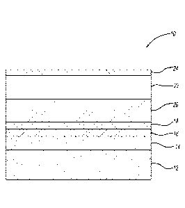
An avalanche photodiode includes a first semiconductor layer, a multiplication layer, a charge control layer, a second semiconductor layer, a graded absorption layer, a blocking layer and a second contact layer. The multiplication layer is located between the charge control layer and the first semiconductor layer. The charge control layer is located between the second semiconductor layer and the multiplication layer. The second semiconductor layer is located between the charge control later and the graded absorption layer. The graded absorption layer is located between the second semiconductor layer and the blocking layer.


French Abstract

La présente invention concerne une photodiode à avalanche qui comprend une première couche semi-conductrice, une couche de multiplication, une couche de commande de charge, une seconde couche semi-conductrice, une couche d'absorption graduelle, une couche de blocage et une seconde couche de contact. La couche de multiplication est située entre la couche de commande de charge et la première couche semi-conductrice. La couche de commande de charge est située entre la seconde couche semi-conductrice et la couche de multiplication. La seconde couche semi-conductrice est située entre la dernière commande de charge et la couche d'absorption graduelle. La couche d'absorption graduelle est située entre la seconde couche semi-conductrice et la couche de blocage.

Claims

Note: Claims are shown in the official language in which they were submitted.


CLAIMS:
1. An avalanche photodiode comprising:
a first semiconductor layer;
a multiplication layer on the first semiconductor layer;
a charge control layer on the multiplication layer, opposite of the first
semiconductor layer;
a second semiconductor layer of indium aluminum arsenide over the
charge control layer, opposite of the multiplication layer;
a graded absorption layer of indium gallium arsenide on the second
semiconductor layer of indium aluminum arsenide, wherein the graded absorption
layer is on a side of the second semiconductor layer opposite of the first
semiconductor
layer, the graded absorption layer having a graded doping concentration and
being in
direct contact with the second semiconductor layer; and
a blocking layer located on the graded absorption layer, wherein the
blocking layer is on a side of the graded absorption layer opposite of the
second
semiconductor layer, wherein:
the graded absorption layer has a cross sectional width less than that of
a cross sectional width of the charge control layer and the multiplication
layer, and
the cross sectional widths of the charge control layer and the
multiplication layer are substantially equal.
2. The avalanche photodiode of claim 1, further comprising a digital grade
layer located between the charge control layer and the second semiconductor
layer.
9

3. The avalanche photodiode of claim 1, wherein the first semiconductor
layer is made of indium phosphide.
4. The avalanche photodiode of claim 3, where the first semiconductor
layer is doped n+.
5. The avalanche photodiode of claim 1, wherein the multiplication layer is
made of indium aluminum arsenide.
6. The avalanche photodiode of claim 1, wherein the graded absorption
layer is made of p+ indium gallium arsenide.
7. The avalanche photodiode of claim 1, wherein the graded absorption
layer is doped p+.
8. The avalanche photodiode of claim 1, further comprising a first contact
adjacent to the first semiconductor layer.
9. The avalanche photodiode of claim 1, wherein the graded absorption
layer is etched to define a small area absorption region on top of the second
semiconductor layer.
10. The avalanche photodiode of claim 9, further comprising a second
contact adjacent to the small area absorption region on top of the second
semiconductor layer.

11. The avalanche photodiode of claim 10, wherein at least a portion of the
avalanche photodiode is passivated with a passivation structure.
12. The avalanche photodiode of claim 11, wherein the passivation structure
is made of benzocyclobutene.
13. The avalanche photodiode of claim 9, further comprising a second
contact adjacent to the small area absorption region on top of the second
semiconductor layer.
14. The avalanche photodiode of claim 1, wherein the graded absorption
layer has a cross sectional width where the graded absorption layer meets the
second
semiconductor layer less than that of a cross sectional width of the second
semiconductor layer where the graded absorption layer meets the second
semiconductor layer.
11

Description

Note: Descriptions are shown in the official language in which they were submitted.


PLANAR AVALANCHE PHOTODIODE
[0001]
BACKGROUND
[0002] The present invention relates to photodetectors. More specifically,
the
present invention relates to avalanche photodiodes ("APDs").
[0003] Owing to the known interaction between photons and electrons,
advances have been made in the field of photodetectors in recent years,
particularly
in those photodetectors that utilize semiconductor materials. One type of
semiconductor-based photodetector known as an avalanche photodiode includes a
number of semiconductive materials that serve different purposes such as
absorption
and multiplication.
[0004] The avalanche photodiode structure provides a large gain through the
action of excited charge carriers that produce large numbers of electron-hole
pairs in
the multiplication layer. In order to prevent tunneling in the absorption
layer, the electric
field is regulated within the avalanche photodiode itself, such that the
electric field in
the multiplication layer is significantly higher than that in the absorption
layer.
[0005] A particular type of avalanche photodiode know as a mesa avalanche
photodiode exposes high field p-n junctions and large numbers of exposed
surface
and interface states that make it difficult to passivate using a layer of
insulating
material. Therefore, conventional InP/InGaAs avalanche photodiodes use
diffused
structures which bury the p-n junction. However, these InP avalanche
photodiodes
require extremely accurate diffusion control of both the depth and the doping
density
1
CA 2873841 2019-05-08

CA 02873841 2014-11-14
WO 2013/176976
PCMJS2013/041536
of the p-type semiconductor regions as well as accurate control of the n-doped
region into which this diffusion occurs. This critical doping control is
essential, since
the diffusion controls the placement of the p-n junction, the magnitude of the
electric
field in the multiplication region, the length of the avalanche region, as
well as the
total charge in the charge control layer which determines the values of the
electric
fields in both the high field InP avalanche region, which must be large enough
to
produce multiplication, as well as the low field InGaAs absorbing region,
which must
be small enough to avoid tunneling. In addition, accurately placed diffused or
implanted guards rings are used in this type of arrangement, to avoid
avalanche
breakdown at the edges of the diffused p-n junction. This combination of guard
rings
and critically controlled diffusions increases the capacitance, lowers the
bandwidth,
and reduces the yield, thus increasing the cost of these APDs.
[0006] For
ultrahigh speed performance detectors, InAlAs can be used as the
avalanche layer rather than InP, since the higher bandgap reduces tunneling
and
thus allows thinner avalanche regions to be used leading to higher speeds and
higher performance receivers. However, a diffused structure is even more
difficult to
achieve in InAlAs since the larger electron avalanche coefficient (relative to
the
holes) makes it desirable to multiply the electrons rather than the holes as
in
standard InP based APDs. Moreover, simply reversing the standard p-doped
diffused structure is not sufficient, since n-dopants do not diffuse fast
enough.
SUMMARY
[0007] In
overcoming the drawbacks of the prior art, the applicant has
discovered that since PIN detectors can be easily passivated with proper
surface
2

CA 02873841 2014-11-14
WO 2013/176976
PCMJS2013/041536
preparation and covered with BOB, to etch the small area p+ InGaAs absorption
region on top of the large area undoped InGaAs absorption layer, and passivate
it
with BOB like a PIN.
[0008] An avalanche
photo diode includes a first semiconductor layer, a
multiplication layer, a charge control layer, a second semiconductor layer, a
graded
absorption layer, and a blocking layer. The multiplication layer is located
between
the first semiconductor layer and the charge control layer. The second
semiconductor layer is located between the charge control layer and the graded
absorption layer. The blocking layer is located adjacent to the graded
absorption
layer, opposite of the second semiconductor layer.
[0009] In another
embodiment, the graded absorption layer may be etched to
find a small area absorption region on top of the second semiconductor layer.
The
avalanche diode may also include a first contact adjacent to the first
semiconductor
layer and a second contact adjacent to the small area absorption region on top
of
the second semiconductor layer.
Additionally, the portion of the avalanche
photodiode may be passivated with a passivation structure, such as BOB.
[0010] Further
objects, features and advantages of this invention will become
readily apparent to persons skilled in the art after a review of the following
description, with reference to the drawings and claims that are appended to
and
form a part of this specification.
BRIEF DESCRIPTION OF THE DRAWINGS
[0011] Figure 1 is
a cross-sectional view of a planar avalanche photodiode in
accordance with the present invention; and
3

[0012] Figure 2 is a cross-sectional view of an alternative planar
avalanche
photodiode in accordance with the present invention.
DETAILED DESCRIPTION
[0013] U.S. Patent No. 7,348,608, contained several innovations including
that
the multiplication layer is buried below the absorption layer; the p+ charge
control layer
extends across the entire large outer mesa but does not increase the
capacitance or
reduce the bandwidth at the operating bias due to the concentration of the
electric field
under the small mini mesa; the absorption layer is grown above the charge
control and
above the multiplication layers; that all these layers have the full large
area of the outer
mesa; and that the small top p+ mini mesa determines the active area and
capacitance
and bandwidth.
[0014] In the U.S. Patent No. 7,348,608 the InGaAs absorption layer is
undoped
and thus depleted at the operating bias. The charge control layer and the
multiplication
layers are also fully depleted at the operating bias. Thus, the small top p+
mini mesa
controls the electric field which is only large directly under this mini mesa.
Thus the
capacitance is small since it is determined by the area of the small mini
mesa.
[0015] The electric field across the depleted absorption layer collects
the
electrons and holes, and determines their transit time, which contributes to
the total
transit time across the entire device and thus determines the overall response
speed.
[0016] U.S. Patent No. 7,078,741 discloses a graded p+ doping in the
InGaAs
absorption layer to
4
CA 2873841 2019-05-08

CA 02873841 2014-11-14
WO 2013/176976
PCMJS2013/041536
increase the responsivity without significantly increasing the transit time or
reducing
the bandwidth. However, this p+ doping layer cannot be simply grown on top of
the
existing APD structure with the same large outer mesa size as the undoped
InGaAs
absorption layer, since it would not be depleted and the large area p+ InGaAs
layer
would create a large capacitance together with the large n+ bottom layer. That
is, the
additional p+ layer must be the same small size as the active region of the
APD in
order to have low capacitance and high bandwidth.
[0017] Referring to
Figure 1, an avalanche photodiode 10 is shown. As its
primary components, the avalanche photodiode 10 includes a first semiconductor
layer 12, a multiplication layer 14, a charge control layer 16, a digital
grade layer 18,
a second semiconductor layer 20, a graded absorption layer 22, and a blocking
layer
24. As shown in Figure 1, the multiplication layer 14 is located between the
charge
control layer 16 and the first semiconductor layer 12. The digital grade layer
18 is
located between the charge control layer 16 and a second semiconductor layer
20.
On top of the second semiconductor layer 20 is a graded absorption layer 22.
On
top of the graded absorption layer 22, is the blocking layer 22.
[0018] The first
semiconductor layer 12 may be an n type semiconductor and
may be selected from a group including tertiary semiconductors, or group III-V
semiconductors. Accordingly, the first semiconductor layer 12 is either two
elements
from group III combined with one element from group V or the converse, two
elements from group V combined with one element from group III. A table of
representative groups of the periodic table is shown below.

CA 02873841 2014-11-14
WO 2013/176976
PCMJS2013/041536
GROUP II GROUP III GROUP IV GROUP V
Zinc (Zn) Aluminum (Al) Silicon (Si) Phosphorus (P)
Cadmium (Cd) Gallium (Ga) Germanium (Ge) Arsenic (As)
Mercury (Hg) Indium (In) Antimony (Sb)
[0019] In certain
embodiments, the first semiconductor layer 12 is InAlAs.
However, it is understood that the first semiconductor layer 12 may be any
binary or
tertiary semiconductor that provides the bandgap for optimized operation of
the
avalanche photodiode 10. The semiconductor multiplication layer 14 may also
selected from a group including tertiary semiconductors, or group III-V
semiconductors. In the preferred embodiment, the semiconductor multiplication
layer 14 is InAlAs.
[0020] The graded
absorption layer 22 is also selected from a group including
tertiary semiconductors, or group III-V semiconductors. In the
preferred
embodiment, the graded absorption layer 22 is InGaAs. However, it is
understood
that both the graded absorption layer 22 and the semiconductor multiplication
layer
14 may be any binary or tertiary semiconductor that provides the bandgap for
optimized operation of the planar avalanche photodiode 10.
[0021] The second
semiconductor layer 20 may also selected from a group
including tertiary semiconductors, or group III-V semiconductors. As before,
the
second semiconductor layer 20 is either two elements from group III combined
with
one element from group V or the converse, two elements from group V combined
with one element from group III. In the
preferred embodiment, the second
semiconductor layer 20 is InAlAs. However, it is understood that the second
6

CA 02873841 2014-11-14
WO 2013/176976
PCT/1JS2013/041536
semiconductor layer 20 may be any binary or tertiary semiconductor that
provides
the bandgap for optimized operation of the avalanche photodiode 10.
[0022] A feature of
the planar avalanche photodiode 10 is that all the critical
layer thicknesses and doping concentrations are regulated in the initial
crystal
growth, and thus are under control, such that they can be reproducibly grown
and
are uniform over the entire wafer. Accordingly, difficulties associated with
process
control during fabrication, particularly those related to the diffusion step,
are not
manifest.
[0023] Referring to
Figure 2, a second embodiment of the avalanche
photodiode 110 is shown. It is first noted that like reference numerals have
been
utilized to refer to like components. For example, first semiconductor layer
112 of
Figure 2 is similar to first semiconductor layer 12 of Figure 1. As in Figure
1, the
avalanche photodiode 110 includes a first semiconductor layer 112, a
multiplication
layer 114, a charge control layer 116, a digital grade layer 118, a second
semiconductor layer 120, a graded absorption layer 122, and a blocking layer
124.
In this embodiment, the avalanche photodiode 110 has been etched. More
specifically, the graded absorption layer 122 has been etched to define a
small area
absorption region 125 on top of the second semiconductor layer 120. Further,
the
avalanche photodiode 110 includes a first contact 126 adjacent to the first
semiconductor layer 112 and a second contact 128 adjacent to the blocking
layer
124. The avalanche photodiode 110 may also have at least a portion being
passivated with a passivation structure 130. The passivation structure may be
made
a BCB.
7

CA 02873841 2014-11-14
WO 2013/176976
PCT/US2013/041536
[0024] Figures 1
and 2 show that the charge control layer 16 or 116, which
can be grown using carbon or Be as the p-dopant, extends across the entire
isolation mesa. In spite of the large area of the p-n junction in this
isolation mesa,
the capacitance above punch-through is not substantially increased. This
occurs
because the device capacitance is (after charge punch-through and depletion)
determined mainly by the area of the small diffused region (photodiode 10) or
etched
p+ region (photodiode 110) and not the isolation mesa, thus leading to a low
capacitance, high speed APD.
[0025] The
photodetectors described above can be implemented as
waveguide photodetectors or as single photon detectors. The photodetectors may
have an integrated lens for improved light collection.
[0026] The forgoing
and other implementations are within the scope of the
following claims. For example,
all n and p doped semiconductors may be
interchanged. That is the n and p doping may be reversed to provide a top mini
mesa of n type semiconductor and a lower contact of a p type.
8

Representative Drawing
A single figure which represents the drawing illustrating the invention.
Administrative Status

2024-08-01:As part of the Next Generation Patents (NGP) transition, the Canadian Patents Database (CPD) now contains a more detailed Event History, which replicates the Event Log of our new back-office solution.

Please note that "Inactive:" events refers to events no longer in use in our new back-office solution.

For a clearer understanding of the status of the application/patent presented on this page, the site Disclaimer , as well as the definitions for Patent , Event History , Maintenance Fee  and Payment History  should be consulted.

Event History

Description Date
Inactive: Late MF processed 2022-05-30
Maintenance Fee Payment Determined Compliant 2022-05-30
Grant by Issuance 2021-01-05
Inactive: Cover page published 2021-01-04
Common Representative Appointed 2020-11-07
Inactive: Final fee received 2020-11-04
Pre-grant 2020-11-04
Letter Sent 2020-07-07
Notice of Allowance is Issued 2020-07-07
Inactive: Approved for allowance (AFA) 2020-05-25
Inactive: QS passed 2020-05-25
Withdraw from Allowance 2020-05-04
Inactive: Application returned to examiner-Correspondence sent 2020-05-04
Inactive: COVID 19 - Deadline extended 2020-04-28
Inactive: Request received: Withdraw from allowance 2020-04-16
Amendment Received - Voluntary Amendment 2020-04-16
Inactive: COVID 19 - Deadline extended 2020-03-29
Notice of Allowance is Issued 2019-12-17
Letter Sent 2019-12-17
Notice of Allowance is Issued 2019-12-17
Common Representative Appointed 2019-10-30
Inactive: Approved for allowance (AFA) 2019-10-29
Inactive: Q2 passed 2019-10-29
Amendment Received - Voluntary Amendment 2019-05-08
Inactive: S.30(2) Rules - Examiner requisition 2018-11-09
Inactive: Report - No QC 2018-11-06
Letter Sent 2018-04-04
Inactive: Multiple transfers 2018-03-22
Letter Sent 2018-02-13
All Requirements for Examination Determined Compliant 2018-02-05
Request for Examination Requirements Determined Compliant 2018-02-05
Request for Examination Received 2018-02-05
Request for Priority Received 2015-03-13
Inactive: Correspondence - PCT 2015-03-13
Inactive: Cover page published 2015-01-20
Inactive: IPC assigned 2014-12-12
Inactive: First IPC assigned 2014-12-11
Inactive: Notice - National entry - No RFE 2014-12-11
Inactive: IPC assigned 2014-12-11
Application Received - PCT 2014-12-11
National Entry Requirements Determined Compliant 2014-11-14
Application Published (Open to Public Inspection) 2013-11-28

Abandonment History

There is no abandonment history.

Maintenance Fee

The last payment was received on 2020-05-04

Note : If the full payment has not been received on or before the date indicated, a further fee may be required which may be one of the following

  • the reinstatement fee;
  • the late payment fee; or
  • additional fee to reverse deemed expiry.

Patent fees are adjusted on the 1st of January every year. The amounts above are the current amounts if received by December 31 of the current year.
Please refer to the CIPO Patent Fees web page to see all current fee amounts.

Fee History

Fee Type Anniversary Year Due Date Paid Date
Basic national fee - standard 2014-11-14
MF (application, 2nd anniv.) - standard 02 2015-05-19 2015-04-13
MF (application, 3rd anniv.) - standard 03 2016-05-17 2016-04-13
MF (application, 4th anniv.) - standard 04 2017-05-17 2017-04-13
Request for examination - standard 2018-02-05
Registration of a document 2018-03-22
MF (application, 5th anniv.) - standard 05 2018-05-17 2018-04-12
MF (application, 6th anniv.) - standard 06 2019-05-17 2019-04-12
2020-04-16 2020-04-16
MF (application, 7th anniv.) - standard 07 2020-05-19 2020-05-04
Final fee - standard 2020-11-09 2020-11-04
MF (patent, 8th anniv.) - standard 2021-05-17 2021-05-03
MF (patent, 9th anniv.) - standard 2022-05-17 2022-05-30
Late fee (ss. 46(2) of the Act) 2022-05-30 2022-05-30
MF (patent, 10th anniv.) - standard 2023-05-17 2023-05-08
MF (patent, 11th anniv.) - standard 2024-05-17 2024-05-06
Owners on Record

Note: Records showing the ownership history in alphabetical order.

Current Owners on Record
MACOM TECHNOLOGY SOLUTIONS HOLDINGS, INC.
Past Owners on Record
BARRY LEVINE
Past Owners that do not appear in the "Owners on Record" listing will appear in other documentation within the application.
Documents

To view selected files, please enter reCAPTCHA code :


To view images, click a link in the Document Description column. To download the documents, select one or more checkboxes in the first column and then click the "Download Selected in PDF format (Zip Archive)" or the "Download Selected as Single PDF" button.

List of published and non-published patent-specific documents on the CPD .

If you have any difficulty accessing content, you can call the Client Service Centre at 1-866-997-1936 or send them an e-mail at CIPO Client Service Centre.


Document
Description 
Date
(yyyy-mm-dd) 
Number of pages   Size of Image (KB) 
Description 2014-11-13 8 282
Abstract 2014-11-13 2 71
Drawings 2014-11-13 2 40
Claims 2014-11-13 3 49
Representative drawing 2014-11-13 1 18
Description 2019-05-07 8 291
Claims 2019-05-07 3 78
Claims 2020-04-15 3 75
Representative drawing 2020-12-06 1 11
Maintenance fee payment 2024-05-05 46 1,908
Notice of National Entry 2014-12-10 1 193
Reminder of maintenance fee due 2015-01-19 1 112
Reminder - Request for Examination 2018-01-17 1 125
Acknowledgement of Request for Examination 2018-02-12 1 187
Commissioner's Notice - Application Found Allowable 2019-12-16 1 503
Curtesy - Note of Allowance Considered Not Sent 2020-05-03 1 406
Commissioner's Notice - Application Found Allowable 2020-07-06 1 551
Courtesy - Acknowledgement of Payment of Maintenance Fee and Late Fee (Patent) 2022-05-29 1 431
Examiner Requisition 2018-11-08 4 231
PCT 2014-11-13 1 53
PCT 2014-11-20 1 35
PCT 2014-11-26 2 87
Correspondence 2015-03-12 4 175
Request for examination 2018-02-04 1 27
Amendment / response to report 2019-05-07 12 373
Withdrawal from allowance 2020-04-15 8 205
Final fee 2020-11-03 1 27