Sélection de la langue

Search

Sommaire du brevet 2873841 

Énoncé de désistement de responsabilité concernant l'information provenant de tiers

Une partie des informations de ce site Web a été fournie par des sources externes. Le gouvernement du Canada n'assume aucune responsabilité concernant la précision, l'actualité ou la fiabilité des informations fournies par les sources externes. Les utilisateurs qui désirent employer cette information devraient consulter directement la source des informations. Le contenu fourni par les sources externes n'est pas assujetti aux exigences sur les langues officielles, la protection des renseignements personnels et l'accessibilité.

Disponibilité de l'Abrégé et des Revendications

L'apparition de différences dans le texte et l'image des Revendications et de l'Abrégé dépend du moment auquel le document est publié. Les textes des Revendications et de l'Abrégé sont affichés :

  • lorsque la demande peut être examinée par le public;
  • lorsque le brevet est émis (délivrance).
(12) Brevet: (11) CA 2873841
(54) Titre français: PHOTODIODE A AVALANCHE PLANE
(54) Titre anglais: PLANAR AVALANCHE PHOTODIODE
Statut: Accordé et délivré
Données bibliographiques
(51) Classification internationale des brevets (CIB):
  • H01L 31/107 (2006.01)
  • H01L 31/0304 (2006.01)
(72) Inventeurs :
  • LEVINE, BARRY (Etats-Unis d'Amérique)
(73) Titulaires :
  • MACOM TECHNOLOGY SOLUTIONS HOLDINGS, INC.
(71) Demandeurs :
  • MACOM TECHNOLOGY SOLUTIONS HOLDINGS, INC. (Etats-Unis d'Amérique)
(74) Agent: MACRAE & CO.
(74) Co-agent:
(45) Délivré: 2021-01-05
(86) Date de dépôt PCT: 2013-05-17
(87) Mise à la disponibilité du public: 2013-11-28
Requête d'examen: 2018-02-05
Licence disponible: S.O.
Cédé au domaine public: S.O.
(25) Langue des documents déposés: Anglais

Traité de coopération en matière de brevets (PCT): Oui
(86) Numéro de la demande PCT: PCT/US2013/041536
(87) Numéro de publication internationale PCT: US2013041536
(85) Entrée nationale: 2014-11-14

(30) Données de priorité de la demande:
Numéro de la demande Pays / territoire Date
61/648,401 (Etats-Unis d'Amérique) 2012-05-17

Abrégés

Abrégé français

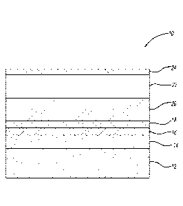
La présente invention concerne une photodiode à avalanche qui comprend une première couche semi-conductrice, une couche de multiplication, une couche de commande de charge, une seconde couche semi-conductrice, une couche d'absorption graduelle, une couche de blocage et une seconde couche de contact. La couche de multiplication est située entre la couche de commande de charge et la première couche semi-conductrice. La couche de commande de charge est située entre la seconde couche semi-conductrice et la couche de multiplication. La seconde couche semi-conductrice est située entre la dernière commande de charge et la couche d'absorption graduelle. La couche d'absorption graduelle est située entre la seconde couche semi-conductrice et la couche de blocage.


Abrégé anglais

An avalanche photodiode includes a first semiconductor layer, a multiplication layer, a charge control layer, a second semiconductor layer, a graded absorption layer, a blocking layer and a second contact layer. The multiplication layer is located between the charge control layer and the first semiconductor layer. The charge control layer is located between the second semiconductor layer and the multiplication layer. The second semiconductor layer is located between the charge control later and the graded absorption layer. The graded absorption layer is located between the second semiconductor layer and the blocking layer.

Revendications

Note : Les revendications sont présentées dans la langue officielle dans laquelle elles ont été soumises.


CLAIMS:
1. An avalanche photodiode comprising:
a first semiconductor layer;
a multiplication layer on the first semiconductor layer;
a charge control layer on the multiplication layer, opposite of the first
semiconductor layer;
a second semiconductor layer of indium aluminum arsenide over the
charge control layer, opposite of the multiplication layer;
a graded absorption layer of indium gallium arsenide on the second
semiconductor layer of indium aluminum arsenide, wherein the graded absorption
layer is on a side of the second semiconductor layer opposite of the first
semiconductor
layer, the graded absorption layer having a graded doping concentration and
being in
direct contact with the second semiconductor layer; and
a blocking layer located on the graded absorption layer, wherein the
blocking layer is on a side of the graded absorption layer opposite of the
second
semiconductor layer, wherein:
the graded absorption layer has a cross sectional width less than that of
a cross sectional width of the charge control layer and the multiplication
layer, and
the cross sectional widths of the charge control layer and the
multiplication layer are substantially equal.
2. The avalanche photodiode of claim 1, further comprising a digital grade
layer located between the charge control layer and the second semiconductor
layer.
9

3. The avalanche photodiode of claim 1, wherein the first semiconductor
layer is made of indium phosphide.
4. The avalanche photodiode of claim 3, where the first semiconductor
layer is doped n+.
5. The avalanche photodiode of claim 1, wherein the multiplication layer is
made of indium aluminum arsenide.
6. The avalanche photodiode of claim 1, wherein the graded absorption
layer is made of p+ indium gallium arsenide.
7. The avalanche photodiode of claim 1, wherein the graded absorption
layer is doped p+.
8. The avalanche photodiode of claim 1, further comprising a first contact
adjacent to the first semiconductor layer.
9. The avalanche photodiode of claim 1, wherein the graded absorption
layer is etched to define a small area absorption region on top of the second
semiconductor layer.
10. The avalanche photodiode of claim 9, further comprising a second
contact adjacent to the small area absorption region on top of the second
semiconductor layer.

11. The avalanche photodiode of claim 10, wherein at least a portion of the
avalanche photodiode is passivated with a passivation structure.
12. The avalanche photodiode of claim 11, wherein the passivation structure
is made of benzocyclobutene.
13. The avalanche photodiode of claim 9, further comprising a second
contact adjacent to the small area absorption region on top of the second
semiconductor layer.
14. The avalanche photodiode of claim 1, wherein the graded absorption
layer has a cross sectional width where the graded absorption layer meets the
second
semiconductor layer less than that of a cross sectional width of the second
semiconductor layer where the graded absorption layer meets the second
semiconductor layer.
11

Description

Note : Les descriptions sont présentées dans la langue officielle dans laquelle elles ont été soumises.


PLANAR AVALANCHE PHOTODIODE
[0001]
BACKGROUND
[0002] The present invention relates to photodetectors. More specifically,
the
present invention relates to avalanche photodiodes ("APDs").
[0003] Owing to the known interaction between photons and electrons,
advances have been made in the field of photodetectors in recent years,
particularly
in those photodetectors that utilize semiconductor materials. One type of
semiconductor-based photodetector known as an avalanche photodiode includes a
number of semiconductive materials that serve different purposes such as
absorption
and multiplication.
[0004] The avalanche photodiode structure provides a large gain through the
action of excited charge carriers that produce large numbers of electron-hole
pairs in
the multiplication layer. In order to prevent tunneling in the absorption
layer, the electric
field is regulated within the avalanche photodiode itself, such that the
electric field in
the multiplication layer is significantly higher than that in the absorption
layer.
[0005] A particular type of avalanche photodiode know as a mesa avalanche
photodiode exposes high field p-n junctions and large numbers of exposed
surface
and interface states that make it difficult to passivate using a layer of
insulating
material. Therefore, conventional InP/InGaAs avalanche photodiodes use
diffused
structures which bury the p-n junction. However, these InP avalanche
photodiodes
require extremely accurate diffusion control of both the depth and the doping
density
1
CA 2873841 2019-05-08

CA 02873841 2014-11-14
WO 2013/176976
PCMJS2013/041536
of the p-type semiconductor regions as well as accurate control of the n-doped
region into which this diffusion occurs. This critical doping control is
essential, since
the diffusion controls the placement of the p-n junction, the magnitude of the
electric
field in the multiplication region, the length of the avalanche region, as
well as the
total charge in the charge control layer which determines the values of the
electric
fields in both the high field InP avalanche region, which must be large enough
to
produce multiplication, as well as the low field InGaAs absorbing region,
which must
be small enough to avoid tunneling. In addition, accurately placed diffused or
implanted guards rings are used in this type of arrangement, to avoid
avalanche
breakdown at the edges of the diffused p-n junction. This combination of guard
rings
and critically controlled diffusions increases the capacitance, lowers the
bandwidth,
and reduces the yield, thus increasing the cost of these APDs.
[0006] For
ultrahigh speed performance detectors, InAlAs can be used as the
avalanche layer rather than InP, since the higher bandgap reduces tunneling
and
thus allows thinner avalanche regions to be used leading to higher speeds and
higher performance receivers. However, a diffused structure is even more
difficult to
achieve in InAlAs since the larger electron avalanche coefficient (relative to
the
holes) makes it desirable to multiply the electrons rather than the holes as
in
standard InP based APDs. Moreover, simply reversing the standard p-doped
diffused structure is not sufficient, since n-dopants do not diffuse fast
enough.
SUMMARY
[0007] In
overcoming the drawbacks of the prior art, the applicant has
discovered that since PIN detectors can be easily passivated with proper
surface
2

CA 02873841 2014-11-14
WO 2013/176976
PCMJS2013/041536
preparation and covered with BOB, to etch the small area p+ InGaAs absorption
region on top of the large area undoped InGaAs absorption layer, and passivate
it
with BOB like a PIN.
[0008] An avalanche
photo diode includes a first semiconductor layer, a
multiplication layer, a charge control layer, a second semiconductor layer, a
graded
absorption layer, and a blocking layer. The multiplication layer is located
between
the first semiconductor layer and the charge control layer. The second
semiconductor layer is located between the charge control layer and the graded
absorption layer. The blocking layer is located adjacent to the graded
absorption
layer, opposite of the second semiconductor layer.
[0009] In another
embodiment, the graded absorption layer may be etched to
find a small area absorption region on top of the second semiconductor layer.
The
avalanche diode may also include a first contact adjacent to the first
semiconductor
layer and a second contact adjacent to the small area absorption region on top
of
the second semiconductor layer.
Additionally, the portion of the avalanche
photodiode may be passivated with a passivation structure, such as BOB.
[0010] Further
objects, features and advantages of this invention will become
readily apparent to persons skilled in the art after a review of the following
description, with reference to the drawings and claims that are appended to
and
form a part of this specification.
BRIEF DESCRIPTION OF THE DRAWINGS
[0011] Figure 1 is
a cross-sectional view of a planar avalanche photodiode in
accordance with the present invention; and
3

[0012] Figure 2 is a cross-sectional view of an alternative planar
avalanche
photodiode in accordance with the present invention.
DETAILED DESCRIPTION
[0013] U.S. Patent No. 7,348,608, contained several innovations including
that
the multiplication layer is buried below the absorption layer; the p+ charge
control layer
extends across the entire large outer mesa but does not increase the
capacitance or
reduce the bandwidth at the operating bias due to the concentration of the
electric field
under the small mini mesa; the absorption layer is grown above the charge
control and
above the multiplication layers; that all these layers have the full large
area of the outer
mesa; and that the small top p+ mini mesa determines the active area and
capacitance
and bandwidth.
[0014] In the U.S. Patent No. 7,348,608 the InGaAs absorption layer is
undoped
and thus depleted at the operating bias. The charge control layer and the
multiplication
layers are also fully depleted at the operating bias. Thus, the small top p+
mini mesa
controls the electric field which is only large directly under this mini mesa.
Thus the
capacitance is small since it is determined by the area of the small mini
mesa.
[0015] The electric field across the depleted absorption layer collects
the
electrons and holes, and determines their transit time, which contributes to
the total
transit time across the entire device and thus determines the overall response
speed.
[0016] U.S. Patent No. 7,078,741 discloses a graded p+ doping in the
InGaAs
absorption layer to
4
CA 2873841 2019-05-08

CA 02873841 2014-11-14
WO 2013/176976
PCMJS2013/041536
increase the responsivity without significantly increasing the transit time or
reducing
the bandwidth. However, this p+ doping layer cannot be simply grown on top of
the
existing APD structure with the same large outer mesa size as the undoped
InGaAs
absorption layer, since it would not be depleted and the large area p+ InGaAs
layer
would create a large capacitance together with the large n+ bottom layer. That
is, the
additional p+ layer must be the same small size as the active region of the
APD in
order to have low capacitance and high bandwidth.
[0017] Referring to
Figure 1, an avalanche photodiode 10 is shown. As its
primary components, the avalanche photodiode 10 includes a first semiconductor
layer 12, a multiplication layer 14, a charge control layer 16, a digital
grade layer 18,
a second semiconductor layer 20, a graded absorption layer 22, and a blocking
layer
24. As shown in Figure 1, the multiplication layer 14 is located between the
charge
control layer 16 and the first semiconductor layer 12. The digital grade layer
18 is
located between the charge control layer 16 and a second semiconductor layer
20.
On top of the second semiconductor layer 20 is a graded absorption layer 22.
On
top of the graded absorption layer 22, is the blocking layer 22.
[0018] The first
semiconductor layer 12 may be an n type semiconductor and
may be selected from a group including tertiary semiconductors, or group III-V
semiconductors. Accordingly, the first semiconductor layer 12 is either two
elements
from group III combined with one element from group V or the converse, two
elements from group V combined with one element from group III. A table of
representative groups of the periodic table is shown below.

CA 02873841 2014-11-14
WO 2013/176976
PCMJS2013/041536
GROUP II GROUP III GROUP IV GROUP V
Zinc (Zn) Aluminum (Al) Silicon (Si) Phosphorus (P)
Cadmium (Cd) Gallium (Ga) Germanium (Ge) Arsenic (As)
Mercury (Hg) Indium (In) Antimony (Sb)
[0019] In certain
embodiments, the first semiconductor layer 12 is InAlAs.
However, it is understood that the first semiconductor layer 12 may be any
binary or
tertiary semiconductor that provides the bandgap for optimized operation of
the
avalanche photodiode 10. The semiconductor multiplication layer 14 may also
selected from a group including tertiary semiconductors, or group III-V
semiconductors. In the preferred embodiment, the semiconductor multiplication
layer 14 is InAlAs.
[0020] The graded
absorption layer 22 is also selected from a group including
tertiary semiconductors, or group III-V semiconductors. In the
preferred
embodiment, the graded absorption layer 22 is InGaAs. However, it is
understood
that both the graded absorption layer 22 and the semiconductor multiplication
layer
14 may be any binary or tertiary semiconductor that provides the bandgap for
optimized operation of the planar avalanche photodiode 10.
[0021] The second
semiconductor layer 20 may also selected from a group
including tertiary semiconductors, or group III-V semiconductors. As before,
the
second semiconductor layer 20 is either two elements from group III combined
with
one element from group V or the converse, two elements from group V combined
with one element from group III. In the
preferred embodiment, the second
semiconductor layer 20 is InAlAs. However, it is understood that the second
6

CA 02873841 2014-11-14
WO 2013/176976
PCT/1JS2013/041536
semiconductor layer 20 may be any binary or tertiary semiconductor that
provides
the bandgap for optimized operation of the avalanche photodiode 10.
[0022] A feature of
the planar avalanche photodiode 10 is that all the critical
layer thicknesses and doping concentrations are regulated in the initial
crystal
growth, and thus are under control, such that they can be reproducibly grown
and
are uniform over the entire wafer. Accordingly, difficulties associated with
process
control during fabrication, particularly those related to the diffusion step,
are not
manifest.
[0023] Referring to
Figure 2, a second embodiment of the avalanche
photodiode 110 is shown. It is first noted that like reference numerals have
been
utilized to refer to like components. For example, first semiconductor layer
112 of
Figure 2 is similar to first semiconductor layer 12 of Figure 1. As in Figure
1, the
avalanche photodiode 110 includes a first semiconductor layer 112, a
multiplication
layer 114, a charge control layer 116, a digital grade layer 118, a second
semiconductor layer 120, a graded absorption layer 122, and a blocking layer
124.
In this embodiment, the avalanche photodiode 110 has been etched. More
specifically, the graded absorption layer 122 has been etched to define a
small area
absorption region 125 on top of the second semiconductor layer 120. Further,
the
avalanche photodiode 110 includes a first contact 126 adjacent to the first
semiconductor layer 112 and a second contact 128 adjacent to the blocking
layer
124. The avalanche photodiode 110 may also have at least a portion being
passivated with a passivation structure 130. The passivation structure may be
made
a BCB.
7

CA 02873841 2014-11-14
WO 2013/176976
PCT/US2013/041536
[0024] Figures 1
and 2 show that the charge control layer 16 or 116, which
can be grown using carbon or Be as the p-dopant, extends across the entire
isolation mesa. In spite of the large area of the p-n junction in this
isolation mesa,
the capacitance above punch-through is not substantially increased. This
occurs
because the device capacitance is (after charge punch-through and depletion)
determined mainly by the area of the small diffused region (photodiode 10) or
etched
p+ region (photodiode 110) and not the isolation mesa, thus leading to a low
capacitance, high speed APD.
[0025] The
photodetectors described above can be implemented as
waveguide photodetectors or as single photon detectors. The photodetectors may
have an integrated lens for improved light collection.
[0026] The forgoing
and other implementations are within the scope of the
following claims. For example,
all n and p doped semiconductors may be
interchanged. That is the n and p doping may be reversed to provide a top mini
mesa of n type semiconductor and a lower contact of a p type.
8

Dessin représentatif
Une figure unique qui représente un dessin illustrant l'invention.
États administratifs

2024-08-01 : Dans le cadre de la transition vers les Brevets de nouvelle génération (BNG), la base de données sur les brevets canadiens (BDBC) contient désormais un Historique d'événement plus détaillé, qui reproduit le Journal des événements de notre nouvelle solution interne.

Veuillez noter que les événements débutant par « Inactive : » se réfèrent à des événements qui ne sont plus utilisés dans notre nouvelle solution interne.

Pour une meilleure compréhension de l'état de la demande ou brevet qui figure sur cette page, la rubrique Mise en garde , et les descriptions de Brevet , Historique d'événement , Taxes périodiques et Historique des paiements devraient être consultées.

Historique d'événement

Description Date
Inactive : TME en retard traitée 2022-05-30
Paiement d'une taxe pour le maintien en état jugé conforme 2022-05-30
Accordé par délivrance 2021-01-05
Inactive : Page couverture publiée 2021-01-04
Représentant commun nommé 2020-11-07
Inactive : Taxe finale reçue 2020-11-04
Préoctroi 2020-11-04
Lettre envoyée 2020-07-07
Un avis d'acceptation est envoyé 2020-07-07
Inactive : Approuvée aux fins d'acceptation (AFA) 2020-05-25
Inactive : QS réussi 2020-05-25
Retirer de l'acceptation 2020-05-04
Inactive : Dem retournée à l'exmntr-Corr envoyée 2020-05-04
Inactive : COVID 19 - Délai prolongé 2020-04-28
Inactive : Dem reçue: Retrait de l'acceptation 2020-04-16
Modification reçue - modification volontaire 2020-04-16
Inactive : COVID 19 - Délai prolongé 2020-03-29
Un avis d'acceptation est envoyé 2019-12-17
Lettre envoyée 2019-12-17
Un avis d'acceptation est envoyé 2019-12-17
Représentant commun nommé 2019-10-30
Inactive : Approuvée aux fins d'acceptation (AFA) 2019-10-29
Inactive : Q2 réussi 2019-10-29
Modification reçue - modification volontaire 2019-05-08
Inactive : Dem. de l'examinateur par.30(2) Règles 2018-11-09
Inactive : Rapport - Aucun CQ 2018-11-06
Lettre envoyée 2018-04-04
Inactive : Transferts multiples 2018-03-22
Lettre envoyée 2018-02-13
Toutes les exigences pour l'examen - jugée conforme 2018-02-05
Exigences pour une requête d'examen - jugée conforme 2018-02-05
Requête d'examen reçue 2018-02-05
Demande de priorité reçue 2015-03-13
Inactive : Correspondance - PCT 2015-03-13
Inactive : Page couverture publiée 2015-01-20
Inactive : CIB attribuée 2014-12-12
Inactive : CIB en 1re position 2014-12-11
Inactive : Notice - Entrée phase nat. - Pas de RE 2014-12-11
Inactive : CIB attribuée 2014-12-11
Demande reçue - PCT 2014-12-11
Exigences pour l'entrée dans la phase nationale - jugée conforme 2014-11-14
Demande publiée (accessible au public) 2013-11-28

Historique d'abandonnement

Il n'y a pas d'historique d'abandonnement

Taxes périodiques

Le dernier paiement a été reçu le 2020-05-04

Avis : Si le paiement en totalité n'a pas été reçu au plus tard à la date indiquée, une taxe supplémentaire peut être imposée, soit une des taxes suivantes :

  • taxe de rétablissement ;
  • taxe pour paiement en souffrance ; ou
  • taxe additionnelle pour le renversement d'une péremption réputée.

Les taxes sur les brevets sont ajustées au 1er janvier de chaque année. Les montants ci-dessus sont les montants actuels s'ils sont reçus au plus tard le 31 décembre de l'année en cours.
Veuillez vous référer à la page web des taxes sur les brevets de l'OPIC pour voir tous les montants actuels des taxes.

Historique des taxes

Type de taxes Anniversaire Échéance Date payée
Taxe nationale de base - générale 2014-11-14
TM (demande, 2e anniv.) - générale 02 2015-05-19 2015-04-13
TM (demande, 3e anniv.) - générale 03 2016-05-17 2016-04-13
TM (demande, 4e anniv.) - générale 04 2017-05-17 2017-04-13
Requête d'examen - générale 2018-02-05
Enregistrement d'un document 2018-03-22
TM (demande, 5e anniv.) - générale 05 2018-05-17 2018-04-12
TM (demande, 6e anniv.) - générale 06 2019-05-17 2019-04-12
2020-04-16 2020-04-16
TM (demande, 7e anniv.) - générale 07 2020-05-19 2020-05-04
Taxe finale - générale 2020-11-09 2020-11-04
TM (brevet, 8e anniv.) - générale 2021-05-17 2021-05-03
TM (brevet, 9e anniv.) - générale 2022-05-17 2022-05-30
Surtaxe (para. 46(2) de la Loi) 2022-05-30 2022-05-30
TM (brevet, 10e anniv.) - générale 2023-05-17 2023-05-08
TM (brevet, 11e anniv.) - générale 2024-05-17 2024-05-06
Titulaires au dossier

Les titulaires actuels et antérieures au dossier sont affichés en ordre alphabétique.

Titulaires actuels au dossier
MACOM TECHNOLOGY SOLUTIONS HOLDINGS, INC.
Titulaires antérieures au dossier
BARRY LEVINE
Les propriétaires antérieurs qui ne figurent pas dans la liste des « Propriétaires au dossier » apparaîtront dans d'autres documents au dossier.
Documents

Pour visionner les fichiers sélectionnés, entrer le code reCAPTCHA :


Pour visualiser une image, cliquer sur un lien dans la colonne description du document. Pour télécharger l'image (les images), cliquer l'une ou plusieurs cases à cocher dans la première colonne et ensuite cliquer sur le bouton "Télécharger sélection en format PDF (archive Zip)" ou le bouton "Télécharger sélection (en un fichier PDF fusionné)".

Liste des documents de brevet publiés et non publiés sur la BDBC .

Si vous avez des difficultés à accéder au contenu, veuillez communiquer avec le Centre de services à la clientèle au 1-866-997-1936, ou envoyer un courriel au Centre de service à la clientèle de l'OPIC.


Description du
Document 
Date
(aaaa-mm-jj) 
Nombre de pages   Taille de l'image (Ko) 
Description 2014-11-13 8 282
Abrégé 2014-11-13 2 71
Dessins 2014-11-13 2 40
Revendications 2014-11-13 3 49
Dessin représentatif 2014-11-13 1 18
Description 2019-05-07 8 291
Revendications 2019-05-07 3 78
Revendications 2020-04-15 3 75
Dessin représentatif 2020-12-06 1 11
Paiement de taxe périodique 2024-05-05 46 1 908
Avis d'entree dans la phase nationale 2014-12-10 1 193
Rappel de taxe de maintien due 2015-01-19 1 112
Rappel - requête d'examen 2018-01-17 1 125
Accusé de réception de la requête d'examen 2018-02-12 1 187
Avis du commissaire - Demande jugée acceptable 2019-12-16 1 503
Courtoisie - Avis d'acceptation considéré non envoyé 2020-05-03 1 406
Avis du commissaire - Demande jugée acceptable 2020-07-06 1 551
Courtoisie - Réception du paiement de la taxe pour le maintien en état et de la surtaxe (brevet) 2022-05-29 1 431
Demande de l'examinateur 2018-11-08 4 231
PCT 2014-11-13 1 53
PCT 2014-11-20 1 35
PCT 2014-11-26 2 87
Correspondance 2015-03-12 4 175
Requête d'examen 2018-02-04 1 27
Modification / réponse à un rapport 2019-05-07 12 373
Retrait d'acceptation 2020-04-15 8 205
Taxe finale 2020-11-03 1 27