Note: Descriptions are shown in the official language in which they were submitted.
81783760
- 1 -
Configurable interface circuit
The invention relates to an interface circuit - also
referred to as interface between a logic
circuit
(logic part of an electrical circuit) and a power
circuit (power part of the circuit), in particular for
use in an aircraft. The power part of the circuit is,
for example, a load to be driven, for example a motor,
which is then connected to a power output of the
interface. Alternatively, it is an electrical element
to be read, for example a switch the switch state of
which is to be detected or a current conductor the
current flow of which is to be measured, said
electrical element then being connected to a power
input of the interface. The interface is generally
connected to a power supply in order to mutually
transform logic signals, which are weak in terms of
power, and load signals, which are intensive in terms
of power.
It is known to use specific DSO (discrete output)
interfaces for the output functionality and to use
specific DSI (discrete input) interfaces for the input
functionality. DSO interfaces in the form of a half-
bridge with semiconductor switches are known. The half-
bridge is driven by the logic part. The centre
connection of the half-bridge forms the power output
for the wiring of the power part. The power supply is
connected to the upper or lower ends of the half-bridge
(supply connection).
It is also known to combine a plurality of interfaces
into an interface module. The interface module then has
a particular number, for example three, of power
outputs, which exclusively have an output function, and
a particular number, for example two, of power inputs,
CA 2874388 2017-10-06
81783760
- 2 -
which exclusively have an input function. A specific DSO interface
is assigned to each of the power outputs and a specific
DSI interface is assigned to each of the power inputs. Such
modules are often used in systems such that at least one of the
connections remains unused. This is disadvantageous, for example
for reasons of cost, resources, space and weight.
It is known from EP 0 620 510 Al to design an interface for
sending and/or receiving digital signals to be configurable. For
this purpose, an Application-Specific Integrated Circuit (ASIC)
is replaced by the combination of a universal microcontroller and
a Field Programmable Gate Array (FPGA) or a comparable circuit.
Such an interface is not suitable for power parts operating using
analog or those with high power, for instance motors or the like.
The problem addressed by the present invention is to specify an
improved interface circuit and an improved interface module.
According to one aspect of the present invention, there is
provided interface circuit for intermediate connection between a
logic circuit and a power circuit, having a supply connection for
connection to a power supply, characterized in that the interface
circuit contains two logic connections to the respective
connection on the logic circuit, which logic connections are
configurable as logic input or logic output, and two power
connections to the respective connection on the power circuit,
which power connections are configurable as power input or power
output, and a configuration unit for configuring the logic
connections and the power connections, wherein the power input
can be read by the logic output and the power output can be
driven by the logic input; wherein interface circuit is designed
as half-bridge circuit, having a switching branch, which is
routed from a first to a second supply connection and which
CA 2874388 2017-10-06
81783760
- 2a -
contains, in a series connection: a first and a second bridge
element, which are each configurable by the configuration unit in
order to be able to be driven by a logic input or to be able to
be read by a logic output, a disconnecting switch, which is
arranged between the first and second bridge element and can be
switched by the configuration unit, the first power connection,
which is arranged between the first bridge element and the
disconnecting switch, the second power connection, which is
arranged between the second bridge element and the disconnecting
switch.
The interface circuit is used for intermediate connection between a
logic circuit and a power circuit. The interface circuit has a
supply connection for connecting to a power supply. The interface
circuit contains two logic connections. Each of the logic
connections is used to connect to a respective logic circuit. Each
of the logic connections is either configurable as logic input or as
logic output. In addition, the interface has two power connections.
Each of the power connections is used in each case to connect to a
power circuit. Each of the power connections is either configurable
as power input or as power output. The interface circuit has a
configuration unit, which is used to configure the logic connections
CA 2874388 2017-10-06
CA 02874388 2014-12-10
- 3 -
and the power connections. In the case of the interface
circuit, each of the power inputs can be read by one of
the logic outputs and each of the power outputs can be
driven by one of the logic inputs.
The described interface circuit represents a minimal
embodiment in terms of the number of logic and power
connections. Further supply, logic or power connections
of the above type mentioned in the sense of the
invention may be present.
The interface circuit offers the advantage that two
power connections are present, which are configurable
as power input or power output according to
requirements and hence can be driven or read. Hence, by
using a sufficient number of identical interface
circuits according to the invention, precisely enough
interfaces can be provided in an electrical system that
the total number of inputs and outputs is covered. If
necessary, a single power connection remains unused.
This results in a reduction in the total number of
interfaces on the system plane by virtue of the
different use possibilities of the interface circuit
which is versatile, that is to say useable in a
versatile manner, and configurable. Thus, the interface
resources are almost completely or completely utilized.
Since an unused interface is present, if necessary, the
space and weight requirement reduces, which is of great
advantage in particular in aircraft technology, and
hence also the costs for the system-wide interfaces.
The interface circuit which can be used in a versatile
manner or is configurable according to requirements is
therefore used to drive loads or motors and to detect
digital and analog signals. By virtue of the
configurability, various functionalities can be
realized as well as various ranges of values of
generated or detected electrical variables.
CA 02874388 2014-12-10
- 4 -
By virtue of the configurability of the power
connections, a desired functionality can be switched on
any of the connections, which ensures a so-called
"switch functionality". In other words, signal routing
within the interface circuit is possible.
Owing to the versatility, it is possible to drive
motors, for example stepper or BLDC (brushless DC)
motors. Measurement functionalities are realizable in
the interface circuit. Thus, autonomous detection of
motor types or configurations can take place. By virtue
of the configuration unit, it is possible to increase
the measurement accuracy within the interface circuit
by, for example, calibration Or temperature
compensation (by software, for example look-up table).
The interface circuit can be used universally. As a
result of the versatility and configurability, there is
a reduction in the range of devices. The interface
circuit can be used universally in various systems. By
virtue of the routing function, there is a reduction in
and optimization of the cabling, in particular in an
aeroplane.
In a preferred embodiment, the interface circuit is
embodied as a half-bridge circuit. Said half-bridge
circuit has a switching branch which is routed from a
first (upper) to a second (lower) supply connection.
The switching branch contains, in a series connection:
a first (upper, TOP, high-side) and a second
(lower, BOT, low-side) bridge element, which are each
configurable by the configuration unit. Depending on
the configuration, each of the bridge elements is able
to be driven by a logic input or able to be read by a
logic output, or otherwise able to be used.
CA 02874388 2014-12-10
- 5 -
- a disconnecting switch, which is arranged between
the first and second bridge element and can be switched
by the configuration unit, that is to say can be opened
or closed;
- the first power connection, which is arranged
between the first bridge element and the disconnecting
switch; and
- the second
power connection, which is arranged
between the second bridge element and the disconnecting
switch.
By virtue of the realization as half-bridge, the known
advantages of half-bridge circuits also emerge for the
interface according to the invention when the
disconnecting switch is closed (conducting). In
particular, a plurality of half-bridges can be combined
to form a full-bridge or even more complex circuits.
For this purpose, the bridge elements are equipped with
a switch function. The two power connections are then
directly connected, with the result that two
connections are physically available for two power
parts. In the case of wiring as digital power input, a
"wired OR" functionality emerges here, which is
externally physically routed to two connections,
however. Thus, in aviation engineering, a permitted
wiring can be performed since the wiring of a single
connection to two lines is forbidden.
By integration of a disconnecting switch in the
"centre" of the half-bridge, the upper (so-called TOP
part) can also be completely disconnected from the
lower (so-called BOT part) half-bridge part. Thus, two
separate circuit parts occur in the interface, which
are connected in each case to one of the power
connections. Both circuit parts can be driven and used
completely separately from one another.
CA 02874388 2014-12-10
- 6 -
Particularly in this embodiment, the abovementioned
switch functionality is possible: by opening or closing
the switch, each of the two power connections can
either be assigned to the TOP or the ROT part of the
half-bridge. In particular, conventional DSO functions
can be routed via the switch functionality: for
example, a DSO high-side can be available at the low-
side power output, or a DSO low-side can be available
at the high-side power output.
The bridge elements as switch elements can be used in
ON, OFF or PWM operation. In PWM operation, current
measurement is also possible in the case of
correspondingly equipped bridge elements. By
corresponding configuration of the disconnecting
switch, current measurement is also possible through
the disconnecting switch via the voltage difference
between the two power connections.
Therefore, a configurable versatile half-bridge
results, which can be used as: DSO high-side and/or DSO
low-side, as a switch, for routing of DSO to various
power outputs (in the form of "pins"), "wired OR
function" for high-side and/or low-side, as isolation
switch for high-side or low-side DSO, as motor
controller, in particular for stepper, BLDC or brush
motors, as DSI with connection to the lower or higher
potential of the power supply (for example DSI-GND-OPEN
and/or DST-28 V-OPEN in the case of a 28 V-supply
voltage) or as analog input (for example from 0 V to
32 V).
A power connection or TOP or BOT branch of the half-
bridge, which connection or branch is not used as
"active" power input or output, can be used as "built-
in test function" (BIT). By way of example, when one
half-bridge part is configured as DSO, the DSI
CA 02874388 2014-12-10
- 7 -
function, which is not used, of the other half-bridge
part can be used as monitoring function of the DSO.
When one half-bridge part is configured as DSI, the DSO
function, which is not used, of the other half-bridge
part can be used to generate a stimulus or a test
function for the DSI function.
In a preferred variant of this embodiment, each of the
bridge elements contains at least one, in particular at
least two series-connected, controllable semiconductor
switches. By using semiconductor switches, many
possibilities of using the electrical main or parasitic
properties of said semiconductor switches in a targeted
manner by targeted wiring or driving using the
configuration unit already present themselves in
relation to the invention. Thus, for example, parasitic
diodes can be used as measuring elements for currents
through the semiconductor switches in question, a
current measurement in PWM operation or a configurable
current limiting in the switching branch can be
realized by driving the semiconductor switch.
In a preferred variant of this embodiment, at least one
of the semiconductor switches contains a MOSFET with
parasitic substrate diode. In particular, if two
MOSFETs are connected in series in a bridge element,
one can primarily be used as switch (diode is actually
"only" parasitic), the other can primarily be used as
controllable diode element (parasitic diode is
"configured" in terms of its properties by the
semiconductor switch).
Therefore, in a preferred variant of this embodiment,
at least one of the semiconductor switches is set up in
a manner connected to the configuration unit such that,
by virtue of said semiconductor switch being driven,
the electrical properties of its parasitic substrate
CA 02874388 2014-12-10
- 8 -
diode as controllable diode are determined in a
targeted manner.
Thus, in particular, a test functionality for checking
the body diodes of the diode-MOSFET, that is to say
testability of the substrate diode by changing the
diode configuration voltage, results. The diode can
also be used as measuring element for the current
through the switch. By configuring the drive of the
diode-FET, the latter is to be used as measuring
resistor or automatic diode/configurable current
measuring element. Two current measuring methods (RDs or
U0s) are possible per configuration. A shift in
measuring ranges or an adaptive measuring range
adaptation are possible. Current limiting is possible
by virtue of linear operation.
In this case, a MOSFET can replace a conventional diode
with nonreactive series resistor. The current through a
switch can be measured via the voltage UGs of the switch
drive. The current measurement for the switch function
is configurable via a regulation of the UGs switch
voltage. The diode can be switched as resistor for a
motor operation. There is minimal current consumption
in the load path. The invention can be used as a device
for measuring a load current in the event of low power
consumption and optimized MTBF and area.
In another preferred embodiment, the disconnecting
switch has two series-connected controllable
semiconductor switches. In particular, the
semiconductor switches each contain MOSFETs with
respective parasitic substrate diodes, wherein the
substrate diodes of said MOSFETs are oriented in
reverse bias with respect to the series connection.
Thus, the abovementioned advantages also emerge for the
disconnecting switch.
CA 02874388 2014-12-10
- 9 -
With respect to the interface module, the problem is
solved by an interface module according to patent claim
8. Said interface module contains at least two power
connections. The interface module contains at least one
interface circuit according to the invention, the power
connections of which interface circuit are routed to
the power connections of the interface module.
The advantages of the interface circuit thus also
emerge for the interface module. In particular, the
module is configurable and therefore can be used in any
way with the result that the power connections thereof
must only be reconfigured and not remain unused when a
particular type of power connection is required in a
system plane.
In a preferred embodiment, additional power connections
in the form of power inputs or outputs are provided in
the module, wherein the interface module contains a
specific input or output interface for each of these
power connections. The power connection is then
permanently embodied as input or output and is not
reconfigurable as output or input. Specific interfaces
such as this are more cost-effective than the universal
interface according to the invention. Since a minimum
number of dedicated power inputs and outputs are
generally required on a system plane anyway, at least
these ones can be realized in a cost-effective manner.
The remaining interfaces can then be provided in a
flexible manner according to the invention.
Further features, effects and advantages of the
invention emerge from the following description of a
preferred exemplary embodiment of the invention and
from the appended figures, in which:
CA 02874388 2014-12-10
- 10 -
Figure 1 shows an interface module according to the
invention having an interface circuit
according to the invention,
Figure 2 shows the interface module from Figure 1 in
an alternative configuration and wiring,
Figure 3 shows the interface circuit from Figures 1
and 2, embodied as a half-bridge,
Figure 4 shows a table of possible configurations of
the half-bridge from Figure 3,
Figure 5 shows possible uses or combinations of the
half-bridge from Figure 3, and
Figure 6 shows the half-bridge circuit from Figure 3
in detail.
Figure 1 shows an interface circuit 2 according to the
invention in an interface module 4, which interface
circuit is interconnected between a logic circuit 6 and
a power circuit 8. The interface circuit is connected
to a power supply 12 via a supply connection 10. Two
logic connections 14a,b are used to connect to the
logic circuit 6, two power connections 16a,b are used
to connect to the power circuit 8 or to a load 18 and a
switch 20. Therefore, the power connection 16a is
configured as power output 22a and the power connection
16b is configured as power input 22b. The logic
connection 14a is configured as logic input 24a for
driving the load 18, the logic connection 14b is
configured as logic output 24b for reading the switch
20. The configuration is done by the configuration unit
26.
The interface module 4 also has power connections 100a-
d. The power connections 16a,b of the interface circuit
CA 02874388 2014-12-10
- 11 -
2 are routed to the power connections 100a,b of the
interface module 4.
The power connections 100c,d are additionally present
on the interface module 4. These are a dedicated input
module 102a and a dedicated output module 102b.
Therefore, the power connection 100c is a power output
for driving a load 18 and the power connection 100d is
a power input for reading a switch 20, which power
connections 100c,d are not reconfigurable as input or
output.
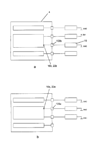
Figure 2a shows the interface module 4 from Figure 1 in
an alternative configuration. Instead of the switch 20,
a load 18 is connected to the power connection 100b.
The power connection 100b and the power connection 16b
are therefore configured as power output 22a.
Figure 2b shows another alternative configuration of
the interface module 4. In this case, as before, the
power connection 16a is configured as power output 22a
but it is configured in this case to drive a load with
respect to ground (GND) instead of with respect to
supply voltage (28V).
Figure 3 shows the interface circuit 2 in the form of a
half-bridge circuit 28 with a switching branch 30 which
is routed from a supply connection 10a connected to the
supply voltage 28V to a supply connection 10b connected
to ground GND. The switching branch contains a series
connection composed of a first bridge element 32a and a
second bridge element 32b with a disconnecting switch
34 lying in between. The first power connection 16a is
located between the first bridge element 32a and the
disconnecting switch 34; the second power connection
16b is located between the second bridge element 32b
and the disconnecting switch 34. The bridge elements
32a,b and the disconnecting switch 34 are configurable
CA 02874388 2014-12-10
- 12 -
by the configuration unit 26. The latter also contains
or is routed to the logic connections 14a,b, which are
not shown in more detail here. The connection lines
shown are used for this purpose.
The bridge elements 34a,b are embodied as a series
connection of in each case two semiconductor switches
36a,b. The semiconductor switch 36a is actually used as
switch 40. The semiconductor switch 36b has a parasitic
diode: said semiconductor switch is driven by the
configuration unit 26 such that the electrical
properties of the diode thereof are used in terms of
circuitry. In other words, the semiconductor switch 36b
is operated or used as configurable diode 38 and not as
an actual switch 40.
In detail, the gate-source voltages UGs of the
semiconductor switches in the bridge elements 32a,b are
controlled, the switching commands of the disconnecting
switch 34 are supplied and the voltages of the line
sections of the switching branch 30 are read via the
connection lines.
Figure 4 shows a table 17 of possible configurations of
the half-bridge circuit 28 (in this case abbreviated to
CVHB: configurable versatile half-bridge) from Figure
3: a maximum of two conventional interface circuits can
be realized per configuration; these are seen in
columns from left to right:
a DSO module for driving a load with respect to
positive supply voltage (for example 28 V)
- a DSO module for driving a load with respect to
negative supply voltage (for example GND)
- a switch
- a stepper motor drive
- a drive for a brushless DC motor (BLDC)
- a drive for a DC motor with brushes (BDC)
CA 02874388 2014-12-10
- 13 -
- a DSI module for inputs with respect to positive
supply voltage (for example 28 V)
- a DSI module for inputs with respect to negative
supply voltage (for example GND)
- an analog
input (for example for voltages from 0
to 32 V) to the first power connection 16a
- an analog input (for example for voltages from 0
to 32 V) to the second power connection 16b.
Figures 5a-c show in each case identical half-bridge
circuits 28 the elements of which, for reasons of
clarity, are numbered only once in a manner
representative of all. Figure 5a shows the half-bridge
circuit 28 when the disconnecting switch 34 is open.
Both the TOP and the BOT part of the half-bridge can be
used to drive loads 18 via the two power connections
16a,b.
Figure 5b shows the combination of two half-bridge
circuits 28 for driving a load 18 between the
respective power connections 16b, wherein current can
be selectively conducted in both directions through the
load.
Figure Sc shows the combination of four half-bridge
circuits 28 for driving a stepper motor or a BLOC motor
as load 18, in each case connected to the power
connections 16b.
Figure 5d likewise shows the combination of four
identical yet alternative half-bridge circuits 28 for
driving a serial bipolar stepper motor as load 18. In
this case, the disconnecting switches 34 are embodied
specifically as a series connection of two
semiconductor switches 36a the parasitic diodes of
which are oriented back-to-back in parallel.
CA 02874388 2014-12-10
- 14 -
Figure 6a shows the TOP part (illustrated in figure 6b
as place holder "HIGH SIDE") of the half-bridge circuit
28; Figure 6b shows the disconnecting switch 34 thereof
(illustrated in figure 6a as place holder "SWITCH") and
EDT part (illustrated in figure 6a as place holder "LOW
SIDE"). The configuration unit 26 is also referred to
as VCIF (versatile configuration interface) in this
case and contains the logic connections 14a,b in the
form of I2C bus connections 42. The references in the
figures are self-explanatory and refer, for example, to
a temperature sensor 44 "TEMP", a monitoring circuit
for monitoring a gate-source voltage "Ucs Sense", an
analog-to-digital converter 46, a microcontroller unit
"MOT", etc.
CA 02874388 2014-12-10
- 15 -
List of reference signs
2 interface circuit
4 interface module
6 logic circuit
8 power circuit
10, 10a,b supply connection
12 power supply
14a,b logic connection
16a,b power connection
18 load
switch
22a power output
15 22b power input
24a logic input
24b logic output
26 configuration unit
28 half-bridge circuit
20 30 switching branch
32a,b bridge element
34 disconnecting switch
36a,b semiconductor switch
38 diode
40 switch
422C bus connection
44 temperature sensor
46 analog-to-digital converter
100a-d power connection
102a input module
102b output module