Note: Descriptions are shown in the official language in which they were submitted.
CA 02874419 2014-11-21
[DESCRIPTION]
[Title of Invention]
CERAMIC MATRIX COMPOSITE COMPONENT COATED WITH ENVIRONMENTAL
BARRIER COATINGS AND METHOD OF MANUFACTURING THE SAME
[Technical Field]
[0001]
The present invention relates to a ceramic matrix
composite component coated with environmental barrier coatings
and a method of manufacturing the same, and particularly to a
ceramic matrix composite component which is used as a
high-temperature component of a jet engine, a rocket engine,
or the like used in a high-temperature gas environment
containing water vapor and a method of manufacturing the same.
[Background Art]
[0002]
In recent years, ceramic matrix composites (CMCs) have
received attention as high-temperature components such as
turbine components and shroud components of jet engines,
thrusters and combustion gas tubes of rocket engines, and the
like used in high-temperature gas environments containing water
vapor because ceramic matrix composites have more excellent
heat resistance and higher specific strength at high
temperature than heat-resistant alloys such as nickel alloys.
[0003]
On the other hand, it has been known that water vapor in
high-temperature gas causes the surface recession of
Si-containing material. In the
case where a
suicide-containing ceramic matrix composite is selected as a
substrate for a high-temperature component, oxidation
resistance and water vapor resistance need to be ensured.
1
CA 02874419 2014-11-21
[0004]
Patent Literature 1 describes a gas turbine engine
combustor component and the like. The gas turbine engine
combustor component includes a substrate formed of
silicon-containing material, an environmental barrier layer
overlaid on the substrate, a transition layer overlaid on the
environmental barrier layer, and a top coat overlaid on the
transition layer.
[Citation List]
[Patent Literature]
[0005]
[PTL 1]
Japanese Patent No. 4901192
[Summary of Invention]
[Technical Problem]
[0006]
High-temperature components such as jet engine turbine
components are exposed to thermal cycles in which high
temperature (for example, component surface temperature is
1200 C to 1400 C) and low temperature (for example, component
surface temperature is 600 C or lower) are repeated, in
high-temperature gas environments containing water vapor (for
example, the partial pressure of water vapor contained in
combustion gas is 30 kPa to 140 kPa).
[0007]
There is a case where a surface of a silicide-containing
ceramic matrix composite is coated with, for example, a
multilayer coating such as described in Patent Literature 1 to
provide oxidation resistance and water vapor resistance to a
high-temperature component. In this case, the delamination of
2
CA 02874419 2014-11-21
the multilayer coating may occur over almost the entire surface
in a short time due to poor adhesion between layers, cyclic
thermal stresses caused by thermal cycles, or the like to impair
the oxidation resistance and the water vapor resistance of the
high-temperature component.
[0008]
Accordingly, an object of the present invention is to
provide a ceramic matrix composite component coated with
environmental barrier coatings which has further improved
oxidation resistance and water vapor resistance even when
exposed to thermal cycles in a high-temperature gas environment
containing water vapor, and a method of manufacturing the same.
[Solution to Problem]
[0009]
A ceramic matrix composite component according to the
present invention is a ceramic matrix composite component
coated with environmental barrier coatings which includes a
substrate formed of a suicide-containing ceramic matrix
composite, a silicon carbide layer deposited on a surface of
the substrate, a silicon layer deposited on a surface of the
silicon carbide layer, a mixed layer made of a mixture of mullite
and ytterbium silicate and deposited on a surface of the silicon
layer, and an oxide layer deposited on a surface of the mixed
layer.
[0010]
In the ceramic matrix composite component according to
the present invention, the ytterbium silicate is any one of
Yb2Si05 and Yb2Si207.
[0011]
In the ceramic matrix composite component according to
3
CA 02874419 2014-11-21
the present invention, the silicon carbide layer has a thickness
of not less than 10 pm nor more than 50 pm, the silicon layer
has a thickness of not less than 50 pm nor more than 140 pm,
and the mixed layer has a thickness of not less than 75 pm nor
more than 225 pm.
[0012]
In the ceramic matrix composite component according to
the present invention, the silicon layer has a thickness of not.
less than 50 pm nor more than 100 pm.
[0013]
In the ceramic matrix composite component according to
the present invention, the oxide layer is formed of oxide mainly
containing at least one selected from the group consisting of
hafnium oxide, hafnium silicate, lutetium silicate, ytterbium
silicate, titanium oxide, zirconium oxide, aluminum titanate,
aluminum silicate, and lutetium hafnium oxide.
[0014]
In the ceramic matrix composite component according to
the present invention, the oxide layer is formed of monoclinic
hafnium oxide.
[0015]
In the ceramic matrix composite component according to
the present invention, the silicon carbide layer is a chemical
vapor deposition coating, the silicon layer and the mixed layer
are thermal sprayed coatings formed by low pressure thermal
spraying, and the oxide layer is a thermal sprayed coating
formed by air thermal spraying.
[0016]
In the ceramic matrix composite component according to
the present invention, the substrate is formed of a ceramic
4
CA 02874419 2014-11-21
matrix composite obtained by combining silicon carbide fibers
with a silicon carbide matrix.
[0017]
In the ceramic matrix composite component according to
the present invention, the ceramic matrix composite component
is used in an environment in which a component surface
temperature is 1200 C to 1400 C and in which water vapor partial
pressure is 30 kPa to 140 kPa.
[0018]
A ceramic matrix composite component manufacturing
method according to the present invention is a method of
manufacturing a ceramic matrix composite component coated with
environmental barrier coatings, the method including: a
substrate forming step of forming a substrate of a
silicide-containing ceramic matrix composite; a silicon
carbide layer deposition step of depositing a silicon carbide
layer on a surface of the substrate by chemical vapor
deposition; a silicon layer deposition step of depositing a
silicon layer on a surface of the silicon carbide layer by low
pressure thermal spraying; a mixed layer deposition step of
depositing a mixed layer made of a mixture of mullite and
ytterbium silicate on a surface of the silicon layer by low
pressure thermal spraying; and an oxide layer deposition step
of depositing an oxide layer on a surface of the mixed layer
by air thermal spraying.
[0019]
In the ceramic matrix composite component manufacturing
method according to the present invention, in the silicon
carbide layer deposition step, the silicon carbide layer is
deposited to a thickness of not less than 10 pm nor more than
1
CA 02874419 2014-11-21
50 pm; in the silicon layer deposition step, the silicon layer
is deposited to a thickness of not less than 50 pm nor more than
140 pm; and, in the mixed layer deposition step, the mixed layer
is deposited to a thickness of not less than 75 pm nor more than
225 pm.
[0020]
In the ceramic matrix composite component manufacturing
method according to the present invention, in the silicon layer
deposition step, the silicon layer is deposited to a thickness
of not less than 50 pm nor more than 100 pm.
[0021]
In the ceramic matrix composite component coated with
environmental barrier coatings which has the above-described
configuration and the method of manufacturing the same, by
coating the surface of the substrate formed of a
silicide-containing ceramic matrix composite with the silicon
carbide layer, the silicon layer, the mixed layer made of a
mixture of mullite and ytterbium silicate, and the oxide layer
which are stacked in this order, the adhesion between the layers
is improved, and the coefficients of thermal expansion of the
layers are graded from the substrate toward the oxide layer to
relieve cyclic thermal stresses caused by thermal cycles.
Accordingly, even in the case where the ceramic matrix composite
component is exposed to thermal cycles in a high-temperature
gas environment containing water vapor, coating delamination
is reduced, and oxidation resistance and water vapor resistance
can be further improved.
[Brief Description of Drawings]
[0022]
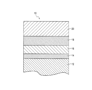
[Fig. 1]
6
CA 02874419 2014-11-21
Fig. 1 is a cross-sectional view showing the
configuration of a ceramic matrix composite component coated
with environmental barrier coatings in an embodiment of the
present invention.
[Fig. 2]
Fig. 2 is a flowchart showing a method of manufacturing
the ceramic matrix composite component coated with
environmental barrier coatings in the embodiment of the present
invention.
[Fig. 3]
Fig. 3 includes graphs showing thermal expansion
characteristics of thermal sprayed coatings in the embodiment
of the present invention.
[Fig. 4]
Fig. 4 is a schematic diagram showing the configuration
of a water vapor exposure tester in the embodiment of the present
invention.
[Fig. 5]
Fig. 5 includes photographs showing the appearances of
specimens of Example 1 after a water vapor exposure test in the
embodiment of the present invention.
[Fig. 6]
Fig. 6 includes a photograph showing the appearance of
a specimen of Example 2 after a water vapor exposure test in
the embodiment of the present invention.
[Fig. 7]
Fig. 7 is a view showing the outline of burner rig testing
in the embodiment of the present invention.
[Fig. 8]
Fig. 8 includes photographs showing results of a burner
7
CA 02874419 2014-11-21
rig test of a specimen of Example 1 after 4000 cycles in the
embodiment of the present invention.
[Fig. 9]
Fig. 9 includes photographs showing results of a burner
rig test of a specimen of Example 2 after 1000 cycles in the
embodiment of the present invention.
[Description of Embodiments]
[0023]
Hereinafter, an embodiment of the present invention will
be described in detail with reference to the drawings. Fig.
1 is a cross-sectional view showing the configuration of a
ceramic matrix composite component 10 coated with environmental
barrier coatings. In the ceramic matrix composite component
10, a surface of a substrate 12 is coated with a silicon carbide
layer 14, a silicon layer 16, a mixed layer 18 made of a mixture
of mullite and ytterbium silicate, and an oxide layer 20 which
are stacked in this order.
[0024]
The substrate 12 is formed of a suicide-containing
ceramic matrix composite. The ceramic matrix composite
includes reinforcing fibers and a ceramic matrix.
[0025]
The reinforcing fibers to be used are, for example,
continuous fibers, discontinuous fibers, or whiskers of silicon
carbide fibers (SiC fibers), silicon nitride fibers (Si3N4
fibers), carbon fibers, graphite fibers, or the like. A preform
to be used is, for example, a fiber fabric having a
three-dimensional structure obtained by bundling several
hundreds to several thousands of filaments of the reinforcing
fibers in fiber bundles and then weaving the fiber bundles in
8
CA 02874419 2014-11-21
XYZ directions, a fabric having a two-dimensional structure
such as a plain weave or satin weave fabric, a unidirectional
material (UD material) , or the like. Moreover, the ceramic
matrix to be used is, for example, silicon carbide, silicon
nitride, or the like.
[0026]
At least either of the reinforcing fibers or the ceramic
matrix is formed of silicide, and both of the reinforcing fibers
and the ceramic matrix may be formed of silicide. Moreover,
the reinforcing fibers and the ceramic matrix may be made of
the same material or different materials. It should be noted
that silicides include silicon as well as silicon-containing
compounds such as silicon carbide and silicon nitride.
[0027]
The ceramic matrix composite to be used is, for example,
a SiC/SiC composite made of silicon carbide fibers and a silicon
carbide matrix, a SiC/Si3N4 composite made of silicon carbide
fibers and a silicon nitride matrix, a Si3N4/Si3N4 composite made
of silicon nitride fibers and a silicon nitride matrix, or the
like. It should be noted that the coefficient of thermal
expansion of a SiC/SiC composite is in the range of 3. Ox10-6/ C
to 4.0x10⁻⁶/ C.
[0028]
The silicon carbide layer 14 is deposited on the surface
of the substrate 12. Since silicon carbide has excellent
oxidation resistance, the oxidation resistance of the substrate
12 can be improved by coating the surface of the substrate 12
with the silicon carbide layer 14. Moreover, since the silicon
carbide layer 14 has a high chemical affinity for the
silicide-containing substrate 12, the adhesive strength
9
CA 02874419 2014-11-21
between the substrate 12 and the silicon carbide layer 14 can
be improved.
[0029]
Further, in the case where the substrate 12 is formed of
a SiC/SiC composite, the thermal expansion difference between
the substrate 12 and the silicon carbide layer 14 is small.
Accordingly, thermal stress is more relieved, and the
occurrence of a fracture in the silicon carbide layer 14 is
reduced. It should be noted that the coefficient of thermal
expansion of silicon carbide is in the range of 3.0x10⁻⁶/ C to
4.0x10⁻⁶/ C.
[0030]
The thickness of the silicon carbide layer 14 may be not
less than 10 pm nor more than 50 pm, may be not less than 20
pm nor more than 40 pm. The reason for this is as follows: if
the thickness of the silicon carbide layer 14 is smaller than
pm, the penetration of oxygen, water vapor, and the like
increases, and oxidation resistance and water vapor resistance
decrease; and, if the thickness of the silicon carbide layer
14 is larger than 50 pm, the occurrence of a fracture in the
silicon carbide layer 14 is more probable because silicon
carbide is a brittle material. Moreover, when the silicon
carbide layer 14 has a thickness of not less than 20 pm nor more
than 40 pm, the penetration of oxygen, water vapor, and the like
is most reduced, and the occurrence of a fracture in the silicon
carbide layer 14 can be most reduced.
[0031]
The silicon carbide layer 14 may be formed of a chemical
vapor deposition coating formed by chemical vapor deposition
(CVD). Since a chemical vapor deposition coating is a denser
CA 02874419 2014-11-21
coating than a thermal sprayed coating and the like, the
penetration of oxygen, water vapor, and the like into the
silicon carbide layer 14 is reduced, and the oxidation and the
water vapor recession of the substrate 12 are more reduced.
[0032]
The silicon layer 16 is deposited on the surface of the
silicon carbide layer 14. The silicon layer 16 serves as a bond
coat for improving the adhesion between the silicon carbide
layer 14 made of non-oxide and the mixed layer 18 made of a
mixture of mullite and ytterbium silicate which are oxides.
Moreover, since the coefficient of thermal expansion of silicon
is close to the coefficient of thermal expansion of silicon
carbide, the occurrence of a fracture due to thermal stress
caused by the thermal expansion difference between the silicon
carbide layer 14 and the silicon layer 16 can be reduced. It
should be noted that the coefficient of thermal expansion of
silicon is in the range of 2.0x10⁻⁶/ C to 3.0x10⁻⁶/ C.
[0033]
The thickness of the silicon layer 16 may be not less than
50 pm nor more than 140 pm, may be not less than 50 pm nor more
than 100 pm, may be not less than 70 pm nor more than 80 pm.
[0034]
The reason for this is as follows: if the thickness of
the silicon layer 16 is smaller than 50 pm, the adhesion between
the silicon carbide layer 14 and the mixed layer 18 decreases;
and if the thickness of the silicon layer 16 is larger than 140
pm, a fracture may occur in the silicon layer 16 because silicon
is a brittle material.
[0035]
Moreover, when the silicon layer 16 has a thickness of
11
CA 02874419 2014-11-21
not more than 100 pm, the occurrence of a fracture in the silicon
layer 16 can be further reduced. Further, when the silicon
layer 16 has a thickness of not less than 70 pm nor more than
80 pm, the adhesion between the silicon carbide layer 14 and
the mixed layer 18 is most improved, and the occurrence of a
fracture in the silicon layer 16 can be most reduced.
[0036]
The silicon layer 16 may be formed of a thermal sprayed
coating formed by low pressure thermal spraying. When the
silicon layer 16 is a thermal sprayed coating formed by low
pressure thermal spraying, the adhesion between the silicon
layer 16 and the silicon carbide layer 14 can be made higher,
and the penetration of oxygen and water vapor is reduced because
a thermal sprayed coating formed by low pressure thermal
spraying is a denser thermal sprayed coating than a thermal
sprayed coating formed by air thermal spraying.
[0037]
The mixed layer 18 made of a mixture of mullite and
ytterbium silicate is deposited on the surface of the silicon
layer 16. The mixed layer 18 improves the adhesion between the
mixed layer 18 and the oxide layer 20, and serves as a stress
relief layer for relieving thermal stress caused by the thermal
expansion differences between both of the silicon carbide layer
14 and the silicon layer 16 and the oxide layer 20.
[0038]
Mullite contained in the mixed layer 18 has the function
of improving the adhesion between the mixed layer 18 and the
oxide layer 20. Further, when mullite and ytterbium silicate
are mixed, the coefficient of thermal expansion of a mixture
of mullite and ytterbium silicate has an approximately
12
CA 02874419 2014-11-21
intermediate value between the coefficients of thermal
expansion of silicon carbide and silicon and the coefficient
of thermal expansion of oxide (5. Ox10-6/ C to 10.0x10⁻⁶/ C) , and
therefore thermal stress caused by the thermal expansion
differences between both of the silicon carbide layer 14 and
the silicon layer 16 and the oxide layer 20 is relieved. For
example, the coefficient of thermal expansion of the mixed layer
18 made of a 1:1 (by volume) mixture of mullite and ytterbium
silicate is in the range of 3.5x10⁻⁶/ C to 4.5x10⁻⁶/ C. Moreover,
since ytterbium silicate has excellent water vapor resistance,
the water vapor resistance of the mixed layer 18 can be made
higher than that of mullite alone.
[0039]
The ytterbium silicate to be used is, for example,
ytterbium monosilicate (Yb2Si05) or ytterbium disilicate
(Yb2Si207) . The mixed layer 18 is formed of a mixture of mullite
(3A1203-2SiO2) and ytterbium monosilicate (Yb2Si05) or a mixture
of mullite (3A1203-2SiO2) and ytterbium disilicate (Yb2Si207) =
[0040]
The thickness of the mixed layer 18 may be not less than
75 pm nor more than 225 pm, may be not less than 75 pm nor more
than 150 pm.
[0041]
The reason for this is as follows: if the thickness of
the mixed layer 18 is smaller than 75 pm, the function thereof
as a stress relief layer decreases due to the small thickness
of the mixed layer 18; and if the thickness of the mixed layer
18 is larger than 225 pm, the occurrence of a fracture in the
mixed layer 18 is more probable because mullite and ytterbium
silicate, which constitute the mixed layer 18, are brittle
13
CA 02874419 2014-11-21
materials. Moreover, when the mixed layer 18 has a thickness
of not less than 75 pm nor more than 150 pm, the function thereof
as a stress relief layer becomes highest, and the occurrence
of a fracture in the mixed layer 18 can be most reduced.
[0042]
The mixed layer 18 may be formed of a thermal sprayed
coating formed by low pressure thermal spraying. When the mixed
layer 18 is a thermal sprayed coating formed by low pressure
thermal spraying, the adhesion between the mixed layer 18 and
the silicon layer 16 can be made higher, and the penetration
of oxygen and water vapor is reduced because a thermal sprayed
coating formed by low pressure thermal spraying is a denser
thermal sprayed coating than a thermal sprayed coating formed
by air thermal spraying.
[0043]
The oxide layer 20 is deposited on the surface of the mixed
layer 18. In general, oxide is excellent in oxidation
resistance, water vapor resistance, and low heat conductivity.
Accordingly, the oxide layer 20 serves as a gas barrier layer
against oxygen, water vapor, and the like, and also serves as
a heat barrier layer against heat transmission from combustion
gas and the like.
[0044]
The oxide layer 20 may be formed of oxide mainly containing
at least one selected from the group consisting of hafnium oxide
(monoclinic Hf02, cubic Hf02, Hf02 stabilized with yttria or the
like, and the like) , hafnium silicate (HfSial and the like) ,
lutetium silicate (Lu2Si05, Lu2Si207, and the like) , ytterbium
silicate (Yb2Si05, Yb2Si207, and the like) , titanium oxide (TiO2
and the like) , zirconium oxide (monoclinic Zr02, cubic Zr02,
14
CA 02874419 2014-11-21
Zr02 stabilized with yttria or the like, and the like) , aluminum
titanate (Al2TiO5 and the like) , aluminum silicate (A16Si2013 and
the like) , and lutetium hafnium oxide (Lu4Hf3012 and the like) .
This is because these oxides are excellent in heat resistance,
oxidation resistance, water vapor resistance, and low heat
conductivity.
[0045]
The oxide layer 20 may be formed of monoclinic hafnium
oxide. This is because monoclinic hafnium oxide has more
excellent water vapor resistance than lutetium silicate,
ytterbium silicate, titanium oxide, aluminum titanate, and the
like, and the coefficient of thermal expansion of monoclinic
hafnium oxide is closer to the coefficients of thermal expansion
of silicon carbide, silicon, and a mixture of mullite and
ytterbium silicate than, for example, the coefficient of
thermal expansion of hafnium oxide stabilized with yttria or
the like is. It should be noted that the coefficient of thermal
expansion of monoclinic hafnium oxide is in the range of
5.0x10⁻⁶/ C to 6.0x10⁻⁶/ C.
[0046]
The thickness of the oxide layer 20 may be not less than
pm nor more than 300 pm, may be not less than 100 pm nor more
than 200 pm.
[0047]
The reason for this is as follows: if the thickness of
the oxide layer 20 is smaller than 10 pm, the penetration of
oxygen, water vapor, and the like increases, and oxidation
resistance and water vapor resistance decrease; and, if the
thickness of the oxide layer 20 is larger than 300 pm, the
occurrence of a fracture in the oxide layer 20 is more probable
CA 02874419 2014-11-21
because oxide is a brittle material. When the oxide layer 20
has a thickness of not less than 100 pm nor more than 200 pm,
oxidation resistance and water vapor resistance are most
improved, and the occurrence of a fracture in the oxide layer
20 can be most reduced.
[0048]
The oxide layer 20 maybe a thermal sprayed coating formed
by air thermal spraying. A thermal sprayed coating formed by
air thermal spraying has more pores than a thermal sprayed
coating formed by low pressure thermal spraying. Accordingly,
when the ceramic matrix composite component 10 is exposed to
heat, the sintering of oxide particles constituting the thermal
sprayed coating is reduced. Thus, the occurrence of a fracture
in the oxide layer 20 can be reduced.
[0049]
Next, a method of manufacturing the ceramic matrix
composite component 10 coated with environmental barrier
coatings will be described.
[0050]
Fig. 2 is a flowchart showing a method of manufacturing
the ceramic matrix composite component 10 coated with
environmental barrier coatings. The method of manufacturing
the ceramic matrix composite component 10 coated with
environmental barrier coatings includes a substrate forming
step (S10), a silicon carbide layer deposition step (S12), a
silicon layer deposition step (S14), a mixed layer deposition
step (S16), and an oxide layer deposition step (S18).
[0051]
The substrate forming step (S10) is the step of forming
the substrate 12 of a suicide-containing ceramic matrix
16
CA 02874419 2014-11-21
composite.
[0052]
The substrate 12 can be formed by a general method of
forming a ceramic matrix composite. For example, the substrate
12 is formed by forming silicon carbide fibers or the like into
a preform such as a three-dimensional fabric and then
infiltrating the preform with a ceramic matrix such as silicon
carbide by chemical vapor deposition (CVD) or CVI (Chemical
Vapor Infiltration) to combine the preform with the ceramic
matrix. The silicon carbide fibers to be used are, for example,
TYRANNO FIBER (manufactured by Ube Industries, Ltd.) ,
HI-NICALON FIBER (manufactured by Nippon Carbon Co., Ltd. ) , or
the like.
[0053]
Instead, the substrate 12 may be formed by infiltrating
the preform with organometallic polymers (precursors of a
ceramic matrix) such as polycarbosilane and then firing the
preform in an inert atmosphere.
[0054]
Another method of forming the substrate 12 may be used
in which the substrate 12 is formed by preparing a mixture of
reinforcing fibers such as silicon carbide fibers and raw
material powders (e.g., silicon powder and carbon powder) for
forming a ceramic matrix of silicon carbide or the like and then
combining the reinforcing fibers and raw material powders by
reaction sintering using a hot press or a hot isostatic press
(HIP) .
[0055]
Moreover, the ceramic matrix composite may be infiltrated
with a slurry containing silicon carbide powder or the like
17
CA 02874419 2014-11-21
dispersed in an organic solvent such as ethanol to fill pores
in the surface of the ceramic matrix composite with silicon
carbide powder or the like and smooth the surface of the
substrate.
[0056]
The silicon carbide layer deposition step (S12) is the
step of depositing the silicon carbide layer 14 on the surface
of the substrate 12.
[0057]
The silicon carbide layer 14 can be formed by thermal
spraying, physical vapor deposition (PVD) such as sputtering
and ion plating, chemical vapor deposition (CVD) , and the like,
but may be formed by chemical vapor deposition because chemical
vapor deposition can form a denser coating than thermal spraying
and the like.
[0058]
In the case where the silicon carbide layer 14 is formed
by chemical vapor deposition, general chemical vapor deposition
for silicon carbide can be used. For example, the silicon
carbide layer 14 can be formed on the surface of the substrate
12 by setting and heating the substrate 12 in a reaction chamber
and introducing methyltrichlorosilane (CH3SiC13) or the like
as reactant gas into the reaction chamber.
[0059]
The silicon layer deposition step (S14) is the step of
depositing the silicon layer 16 on the surface of the silicon
carbide layer 14.
[0060]
The silicon layer 16 can be formed by thermal spraying,
physical vapor deposition (PVD) , chemical vapor deposition
18
CA 02874419 2014-11-21
(CVD) , and the like, but thermal spraying (air thermal spraying
or low pressure thermal spraying) can form a coating having good
adhesion. The thermal spraying to be used is general plasma
spraying or the like.
[0061]
With regard to the thermal spraying to be used, low
pressure thermal spraying can cause less oxidation of the
silicon carbide layer 14 and less oxidation of silicon powder
as thermal spraying material and can form a denser thermal
sprayed coating than air thermal spraying. For example,
procedures for forming the silicon layer 16 by low pressure
thermal spraying are as follows: the substrate 12 coated with
the silicon carbide layer 14 is set in a thermal spraying chamber,
and the thermal spraying chamber is evacuated to a vacuum; then,
in a vacuum state or in a state obtained by introducing inert
gas such as argon gas and reducing the pressure, silicon powder
is fed to a thermal spray gun; and thermal spraying is performed
on the surface of the silicon carbide layer 14. The thermal
spraying material to be used is, for example, silicon powder
having grain sizes of 10 pm to 40 pm.
[0062]
The mixed layer deposition step (S16) is the step of
depositing the mixed layer 18 made of a mixture of mullite and
ytterbium silicate on the surface of the silicon layer 16.
[0063]
The mixed layer 18 can be formed by thermal spraying,
physical vapor deposition (PVD) , chemical vapor deposition
(CVD) , and the like, but thermal spraying (air thermal spraying
or low pressure thermal spraying) can form a coating having good
adhesion. With regard to the thermal spraying to be used, low
19
CA 02874419 2014-11-21
pressure thermal spraying can cause less oxidation of the
silicon layer 16 and can form a denser thermal sprayed coating
than air thermal spraying.
[0064]
In the case where the mixed layer 18 is formed by low
pressure thermal spraying, mixed powder obtained by mixing
mullite powder and ytterbium silicate powder in advance may be
used as thermal spraying material, the mixed powder being fed
to a thermal spray gun and thermal sprayed onto the surface of
the silicon layer 16 in a vacuum or reduced-pressure state; or
mullite powder and ytterbium silicate powder may be separately
fed to a thermal spray gun to be mixed in a melted or near-melted
state and thermal sprayed in a vacuum or reduced-pressure state.
The thermal spraying materials to be used are, for example,
mullite powder and ytterbium silicate powder having grain sizes
of 10 pm to 50 pm.
[0065]
The oxide layer deposition step (S18) is the step of
depositing the oxide layer 20 on the surface of the mixed layer
18.
[0066]
The oxide layer 20 can be formed by thermal spraying,
physical vapor deposition (PVD) , chemical vapor deposition
(CVD) , and the like, but thermal spraying (air thermal spraying
or low pressure thermal spraying) can form a coating having good
adhesion. With regard to the thermal spraying to be used, air
thermal spraying can cause less sintering of oxide particles
constituting the thermal sprayed coating.
[ 0067 ]
For example, procedures for forming the oxide layer 20
CA 02874419 2014-11-21
by air thermal spraying are as follows: the substrate 12 having
the surface thereof coated with the mixed layer 18 is set in
a thermal spraying chamber; oxide powder as thermal spraying
material is fed to a thermal spray gun; and thermal spraying
is performed on the surface of the mixed layer 18 in an
atmospheric-pressure state. The thermal spraying material to
be used is, for example, oxide powder having grain sizes 10 pm
to 50 pm. Thus, the manufacturing of the ceramic matrix
composite component 10 coated with environmental barrier
coatings is completed.
[0068]
In the above-described configuration, by coating the
surface of the substrate formed of the silicide-containing
ceramic matrix composite with the silicon carbide layer, the
silicon layer, the mixed layer made of a mixture of mullite and
ytterbium silicate, and the oxide layer which are stacked in
this order, the adhesive strength between the layers are
improved, and the respective coefficients of thermal expansion
of the layers are graded from the substrate toward the oxide
layer to relieve cyclic thermal stresses caused by thermal
cycles. Accordingly, even in the case where the ceramic matrix
composite component is exposed to thermal cycles in a
high-temperature gas environment containing water vapor,
coating delamination is reduced, and oxidation resistance and
water vapor resistance can be more improved.
[0069]
Moreover, by adjusting the thickness of each layer such
that the thickness of the silicon carbide layer is not less than
pm nor more than 50 pm, the thickness of the silicon layer
is not less than 50 pm nor more than 140 pm, and the thickness
21
CA 02874419 2014-11-21
of the mixed layer is not less than 75 pm nor more than 225 pm,
coating delamination is reduced, and oxidation resistance and
water vapor resistance can be more improved even in the case
where the ceramic matrix composite component is exposed to a
high-temperature environment containing water vapor (surface
temperature 1300 C, water vapor partial pressure 150 kPa) for
100 hours, or even in the case where the ceramic matrix composite
component is exposed to 1000 thermal cycles (surface
temperature ranges from below 600 C to 1300 C)
[0070]
Further, by adjusting the thickness of each layer such
that the thickness of the silicon carbide layer is not less than
pm nor more than 50 pm, the thickness of the silicon layer
is not less than 50 pm nor more than 100 pm, and the thickness
of the mixed layer is not less than 75 pm nor more than 225 pm,
coating delamination and fracture are reduced, and oxidation
resistance and water vapor resistance can be further improved
even in the case where the ceramic matrix composite component
is exposed to a high-temperature environment containing water
vapor (surface temperature 1300 C, water vapor partial pressure
150 kPa) for 800 hours, or even in the case where the ceramic
matrix composite component is exposed to 4000 thermal cycles
(surface temperature ranges from below 600 C to 1300 C).
[Examples]
[0071]
Specimens coated with environmental barrier coatings
were prepared, and water vapor exposure tests and burner rig
tests were conducted to evaluate water vapor characteristics
and thermal cycle characteristics.
[0072]
22
I
CA 02874419 2014-11-21
(Specimen Preparation)
First, methods of preparing specimens of Examples 1 and
2 will be described. It should be noted that the specimens of
Examples 1 and 2 have the same configuration, except for the
thickness of the Si layer.
[0073]
Substrates of the specimens of Examples 1 and 2 were formed
of a SiC/SiC composite obtained by combining SiC fibers and a
SiC matrix. The SiC/SiC composite was formed by infiltrating
a preform formed of SiC fibers with silicon powder and carbon
powder and forming a SiC matrix by reaction sintering to obtain
a composite material. As the SiC fibers, TYRANNO FIBER
(manufactured by Ube Industries, Ltd.) was used. Moreover, the
SiC/SiC composite was infiltrated with a slurry containing
silicon carbide powder dispersed in ethanol to fill pores in
the surface of the SiC/SiC composite with silicon carbide powder
and smooth the surface of the substrate. For water vapor
exposure tests, the substrate had a tapered flat shape of 50
mm x 9mm x 4 mint or a flat shape of 50 mm x 35 mmx 4 mmt having
edges rounded with a radius of 1.5 mm. For burner rig tests,
the substrate had a flat shape of 50 mm x 50 mm x 4 mint.
[0074]
Next, a SiC layer was deposited on the surface of the
substrate by CVD. The substrate was set in a reaction chamber
and heated (reaction temperature was 900 C to 1000 C), and
methyltrichlorosilane (CH3SiC13) was used as reactant gas.
Thus, the surface of the substrate was coated with a SiC layer.
The thickness of the SiC layer was 30 pm in the specimens of
both of Examples 1 and 2.
[0075]
23
CA 02874419 2014-11-21
Next, a Si layer was deposited on the surface of the SiC
layer by low pressure thermal spraying. The substrate coated
with the SiC layer was set in a thermal spraying chamber, and
the thermal spraying chamber was evacuated to a vacuum. Then,
argon gas was introduced into the thermal spraying chamber, and
melted Si powder was thermal sprayed onto the surface of the
SiC layer in a state in which the pressure in the thermal spraying
chamber was reduced. The grain sizes of the Si powder used were
20 pm to 40 pm. The thickness of the Si layer was 75 pm in the
specimens of Example 1 and 140 pm in the specimens of Example
2. It should be noted that the thickness of the Si layer was
adjusted by changing thermal spraying time.
[ 007 6 ]
Next, a mixed layer of 3A1203 .2Si02 and Yb2Si05 was
deposited on the surface of the Si layer by low pressure thermal
spraying. In the low pressure thermal spraying, mixed powder
(powder having a mixing ratio adjusted so that the volume ratio
after the formation of the thermal sprayed coating may be 1:1)
of 3A1203 -2Si02 powder and Yb2Si05 powder was used as thermal
spraying material, and the mixed powder melted was thermal
sprayed onto the surface of the Si layer in a state in which
the pressure in the thermal spraying chamber containing argon
gas was reduced. The thickness of the mixed layer of
3A1203 .2Si02 and Yb2Si05 was 75 pm in the specimens of both of
Examples 1 and 2.
[0077]
Next, a Hf02 layer was deposited on the surface of the
mixed layer of 3A1203 -2Si02 and Yb2Si05 by air thermal spraying.
Powder of Hf02 was fed to a thermal spray gun, and the Hf02 powder
melted was thermal sprayed onto the surface of the mixed layer
24
CA 02874419 2014-11-21
of 3A1203 .2Si02 and Yb2Si05 in an atmospheric-pressure state.
The Hf02 powder used was monoclinic Hf02 powder. The thickness
of the Hf02 layer was 150 pm in the specimens of both of Examples
1 and 2.
[0078]
In the above-described specimens of Examples 1 and 2,
after the deposition of the Hf02 layers, visual inspection was
performed, and fracture and delamination were not observed in
the coatings.
[0079]
(Thermal Expansion Measurement)
Test pieces simulating a Si layer, a mixed layer of
3A1203 .2Si02 and Yb2Si05, and a Hf02 layer were prepared, and
thermal expansion measurement was conducted in the temperature
range of room temperature to 1200 C.
[0080]
A test piece simulating a Si layer was prepared by low
pressure thermal spraying using Si powder as thermal spraying
material, and thermal expansion measurement was conducted in
accordance with the measurement method defined in JIS Z2285.
As a result, the coefficient of thermal expansion of the test
piece simulating a Si layer was in the range of 2.0x10⁻⁶/ C to
2.5x10⁻⁶/ C.
[0081]
A test piece simulating a mixed layer of 3A1203 .2Si02 and
Yb2Si05 was prepared by low pressure thermal spraying using
mixed powder (powder having a mixing ratio adjusted so that the
volume ratio after the formation of the thermal sprayed coating
may be 1:1) of 3A1203 .2Si02 powder and Yb2Si05 powder as thermal
spraying material, and thermal expansion measurement was
CA 02874419 2014-11-21
conducted. Moreover, for the sake of comparison, a test piece
was prepared using 3A1203.2Si02 powder as thermal spraying
material, and thermal expansion measurement was conducted.
[0082]
Fig. 3 includes graphs showing thermal expansion
characteristics of thermal sprayed coatings. Fig. 3(a) is a
graph showing thermal expansion characteristics of the thermal
sprayed coating made of 3A1203.2Si02, and Fig. 3(b) is a graph
showing thermal expansion characteristics of the thermal
sprayed coating made of a mixture of 3A1203.2Si02 and Yb2Si05.
[0083]
As shown in Fig. 3(a), in the case of the thermal sprayed
coating made of 3A1203.2Si02, at temperatures above 900 C,
volume shrinkage occurs due to the sintering of 3A1203.2Si02
particles constituting the thermal sprayed coating, and the
thermal expansion ratio significantly decreases.
[0084]
On the other hand, as shown in Fig. 3(b), in the case of
the thermal sprayed coating made of a mixture of 3A1203.2Si02
and Yb2Si05, at temperatures above 900 C, the volume shrinkage
caused by the sintering of 3A1203 .2Si02 particles in the thermal
sprayed coating is reduced, and the decrease in the thermal
expansion ratio is reduced.
[0085]
As described above, with a mixed layer made of a mixture
of mullite and ytterbium silicate, the great decrease in the
thermal expansion ratio can be made smaller than that of mullite
alone at temperatures above 900 C. The coefficient of thermal
expansion of the test piece simulating a mixed layer of
3A1203.2S102 and Yb2Si05 was in the range of 3.5x10⁻⁶/ C to
26
CA 02874419 2014-11-21
4.5x10⁻⁶/ C.
[0086]
A test piece simulating a Hf02 layer was prepared by air
thermal spraying using monoclinic Hf02 powder as thermal
spraying material, and thermal expansion measurement was
conducted. As a result, the coefficient of thermal expansion
of the test piece simulating a Hf02 layer was in the range of
5.0x10⁻⁶/ C to 6.0x10⁻⁶/ C.
[0087]
As described above, in each of the specimens of Examples
1 and 2, the coefficient of thermal expansion of the mixed layer
made of a mixture of 3A1203-2SiO2 and Yb2Si05 has an intermediate
value between the coefficient of thermal expansion of the Si
layer and the coefficient of thermal expansion of the Hf02 layer.
[0088]
(Water Vapor Exposure Test)
Water vapor exposure tests were conducted on specimens
of Examples 1 and 2. Moreover, as specimens of a comparative
example, a water vapor exposure test was conducted on a
substrate with no environmental barrier coatings (substrate
alone which is formed of a SiC/SiC composite) .
[0089]
First, a method for conducting a water vapor exposure test
will be described. For water vapor exposure testing, a water
vapor exposure tester fabricated by Toshin Kogyo Co., Ltd. was
used. Specifications of this water vapor exposure tester are
as follows: the maximum temperature is 1500 C (working
temperature 1400 C) , and the maximum pressure in a test chamber
is 950 kPa (9.5 atm) .
[0090]
27
CA 02874419 2014-11-21
Fig. 4 is a schematic diagram showing the configuration
of a water vapor exposure tester 30. Around a test chamber 32
made of alumina, a heater 34 made of MoSi2 is provided. In the
test chamber 32, the following components are provided: a water
vapor feed pipe 36 for feeding water vapor, an atmospheric gas
feed pipe 38 for feeding atmospheric gas (air, nitrogen, oxygen,
or carbon dioxide gas) , a mixed gas discharge pipe 40 for
discharging mixed gas from the test chamber, and a thermocouple
42 for temperature control. Moreover, a specimen 44 is placed
in the test chamber 32 such that water vapor fed from the water
vapor feed pipe 36 flows along the surface of the specimen.
[0091]
Test conditions for water vapor exposure testing were as
follows: test temperature was 1300 C, the total pressure in the
test chamber was 950 kPa (9.5 atm) , the partial pressure of water
vapor was 150 kPa (1.5 atm) , and the partial pressure of
atmospheric gas (02+N2+CO2) was 800 kPa (8 atm) . Water vapor
exposure test evaluation was performed by visual inspection.
[0092]
Fig. 5 includes photographs showing the appearances of
the specimens of Example 1 subjected to a water vapor exposure
test. Visual inspections were performed after 270 hours, 500
hours, and 800 hours of water vapor exposure. In the specimens
of Example 1, even after 800 hours of water vapor exposure,
fracture and delamination were not observed in the coatings.
It should be noted that with regard to front and back surfaces
of a specimen, the surface of the specimen facing the water vapor
feed pipe was regarded as the front surface (specimen surface
44A in Fig. 4) , and the surface of the specimen opposite to the
front surface was regarded as the back surface (specimen surface
28
CA 02874419 2014-11-21
44B in Fig. 4).
[0093]
Fig. 6 includes a photograph showing the appearance of
the specimen of Example 2 subjected to a water vapor exposure
test. In the specimen of Example 2, after 100 hours of water
vapor exposure, slight fracture was observed in an edge portion,
but coating delamination did not occur.
[0094]
It should be noted that the specimen of the comparative
example was corroded by water vapor exposure after 60 hours of
water vapor exposure, to such an extent that the shape thereof
was not maintained.
[0095]
(Burner Rig Test)
Burner rig tests were conducted on the specimens of
Examples 1 and 2. First, a method for conducting a burner rig
test will be described. Fig. 7 is a view showing the outline
of burner rig testing. Fig. 7(a) is a schematic diagram
schematically showing the configuration of a burner rig tester
50, and Fig. 7(b) is a view showing specimen surface temperature
cycle conditions for one cycle.
[0096]
As shown in Fig. 7(a), a burner rig test is conducted with
a specimen 54 held on a holder 52 and with flame from a nozzle
56 pointed at a specimen surface. The surface temperature of
the specimen 54 is measured with a radiation thermometer (not
shown). The position at which the surface temperature of the
specimen 54 is measured with the radiation thermometer is in
a central portion of the specimen 54. With regard to the
calibration of specimen surface temperature by the radiation
29
CA 02874419 2014-11-21
thermometer, blackbody paint was applied to the specimen 54 in
advance, and the emissivity of the specimen 54 was adjusted.
Moreover, a camera capable of taking photographs of the coating
surface is installed so that the coating surface can be
photographed and observed during thermal cycles.
[0097]
The specimen 54 was set on the holder 52 and subjected
to thermal cycles. Each cycle consists of 45-second heating
(from below 600 C to 1250 C) , 45-second holding (from 1250 C
to 1300 C) , and 90-second cooling (from 1300 C to below 600 C)
as shown in Fig. 7 (b) .
[0098]
Burner rig test evaluation was performed by visual
inspection and cross-section observation. It should be noted
that in cross-section observation, a sample cut out of a
specimen after a burner rig test was embedded in embedding resin,
then polished, and observed with an optical microscope.
[0099]
Fig. 8 includes photographs showing burner rig test
results of a specimen of Example 1 after 4000 cycles. Fig. 8(a)
is a photograph showing a result of visual inspection, and Fig.
8(b) is a photograph showing a result of cross-section
observation.
[0100]
In the specimen of Example 1, as can be seen from the result
of visual inspection shown in Fig. 8 (a) , fracture and
delamination were not observed in the coatings even after 4000
cycles. Moreover, as can be seen from the result of
cross-section observation shown in Fig. 8 (b) , microcracks were
observed in the Hf02 layer and the mixed layer of 3A1203.2Si02
CA 02874419 2014-11-21
and Yb2Si05 in the thickness direction, but the occurrence of
microcracks was not observed in the Si layer and the SiC layer.
It should be noted that in the photograph in Fig. 8 (a) showing
the result of visual inspection, black portions of the specimen
surface are portions to which blackbody paint was applied.
[0101]
Fig. 9 includes photographs showing burner rig test
results of a specimen of Example 2 after 1000 cycles. Fig. 9(a)
is a photograph showing a result of visual inspection, and Fig.
9(b) is a photograph showing a result of cross-section
observation.
[0102]
In the specimen of Example 2, as can be seen from the result
of visual inspection shown in Fig. 9 (a) , slight fracture was
observed in coatings in an edge portion after 1000 cycles, but
coating delamination did not occur. As can be seen from the
result of cross-section observation shown in Fig. 9 (b) ,
microcracks were observed in the Hf02 layer and the mixed layer
of 3A1203 -2Si02 and Yb2Si05 in the thickness direction, and the
occurrence of a microcrack was observed in the Si layer in a
horizontal direction (in-plane direction) . Moreover, the
occurrence of a microcrack was not observed in the SiC layer.
[Industrial Applicability]
[0103]
In the present invention, even in the case where the
ceramic matrix composite component is exposed to thermal cycles
in a high-temperature gas environment containing water vapor,
coating delamination is reduced, and oxidation resistance and
water vapor resistance can be improved. Accordingly, the
present invention is useful in high-temperature components of
31
I
CA 02874419 2014-11-21
jet engines, rocket engines, and the like.
32