Note: Descriptions are shown in the official language in which they were submitted.
CA 02874551 2014-11-21
WO 2013/180946 PCT/US2013/040950
JOSEPHSON MAGNETIC MEMORY CELL SYSTEM
TECHNICAL FIELD
[0001] The present invention relates generally to quantum and classical
digital
superconducting circuits, and specifically to a Josephson magnetic memory cell
system.
BACKGROUND
[0002] Superconducting digital technology has provided computing and/or
communications resources that benefit from unprecedented high speed, low power
dissipation, and low operating temperature. For decades, superconducting
digital technology
has lacked random-access memory (RAM) with adequate capacity and speed
relative to logic
circuits. This has been a major obstacle to industrialization for current
applications of
superconducting technology in telecommunications and signal intelligence, and
can be
especially forbidding for high-end computing. All concepts currently
considered for
superconducting memory have been based on quantization of magnetic flux quanta
in a
superconducting inductive loop. Such memories can be readily adapted to high
speed register
files given a foundry process with adequate yield, but can never achieve the
integration
density of complementary metal-oxide semiconductor (CMOS), as they are
fundamentally
limited by the size of the inductive loop.
SUMMARY
[0003] One aspect of the present invention includes a Josephson magnetic
memory
cell system. The system includes at least one superconducting electrode
configured to
conduct a read current. The system also includes at least one hysteretic
magnetic Josephson
junction (HMJJ). At least one of the at least one HMJJ is configured to store
a binary value
and to convert superconducting pairs associated with the read current flowing
through the at
least one of the at least one HMJJ from a singlet-state to a triplet-state.
The system further
includes a write circuit magnetically coupled to at least one of the at least
one HMJJ and
configured to write the binary value into the at least one of the at least one
HMJJ in response
to at least one write current and a read circuit configured to determine the
binary value stored
1
CA 02874551 2014-11-21
WO 2013/180946 PCT/US2013/040950
in the at least one of the at least one HMJJ in response to application of the
read current to the
at least one of the at least one HMJJ.
[0004] Another aspect of the present invention includes a Josephson
magnetic
memory cell system. The system includes at least one superconducting electrode
configured
to conduct a read current. The system also includes an HMJJ comprising at
least one first
magnetic material layer having a fixed magnetization and at least one second
magnetic
material layer having a free magnetization corresponding to a bi-stable
orientation. At least
one of the at least one first magnetic material layer and the at least one
second magnetic
material layer has a substantially orthogonal magnetic polarity with respect
to remaining
magnetic material layers. The HMJJ is configured to store a binary value based
on the
magnetic polarity of at least one of the at least one first and the at least
one second magnetic
material layers. The system further includes a write circuit magnetically
coupled to the HMJJ
and configured to write the binary value into the HMJJ in response to at least
one write
current and a read circuit configured to determine the binary value stored in
the HMJJ in
response to application of the read current to the HMJJ.
[0005] Another aspect of the present invention includes a Josephson
magnetic random
access memory (JMRAM) comprising a plurality of Josephson magnetic memory cell
systems arranged as an array of rows and columns. Each of the Josephson
magnetic memory
cell systems includes an HMJJ comprising at least one first magnetic material
layer having a
fixed magnetization and at least one second magnetic material layer having a
free
magnetization corresponding to a bi-stable orientation. At least one of the at
least one first
magnetic material layer and at least one second magnetic material layer has a
substantially
orthogonal magnetic polarity with respect to remaining magnetic material
layers to convert
superconducting pairs associated with the read current flowing through the
HMJJ from a
singlet-state to a triplet-state in the respective HMJJ. Each of the HMJJs are
configured to
store a respective binary value in response to a word-write current that is
provided on a word-
write line and a bit-write current that is provided on a bit-write line to
adjust the magnetic
polarity of at least one of the at least one second magnetic material layer.
Each of the HMJJs
are further configured to output the respective binary value in response to a
word-read current
that is provided on a word-read line and a bit-read current that is provided
on a bit-read line.
2
CA 02874551 2014-11-21
WO 2013/180946
PCT/US2013/040950
BRIEF DESCRIPTION OF THE DRAWINGS
[0006] FIG. 1 illustrates an example of a Josephson magnetic memory cell
system in
accordance with an aspect of the invention.
[0007] FIG. 2 illustrates an example of a hysteretic magnetic Josephson
junction
(HMJJ) in accordance with an aspect of the invention.
[0008] FIG. 3 illustrates an example of a diagram of two states of an
HMJJ in
accordance with an aspect of the invention.
[0009] FIG. 4 illustrates another example of a diagram of two states of
an HMJJ in
accordance with an aspect of the invention.
[0010] FIG. 5 illustrates another example of a HMJJ in accordance with an
aspect of
the invention
[0011] FIG. 6 illustrates yet another example of a diagram of two states
of an HMJJ
in accordance with an aspect of the invention
[0012] FIG. 7 illustrates an example of a Josephson magnetic random
access memory
(JMRAM) system in accordance with an aspect of the invention.
DETAILED DESCRIPTION
[0013] The present invention relates generally to quantum and classical
digital
superconducting circuits, and specifically to a Josephson magnetic memory cell
system. A
Josephson magnetic memory cell system can include a hysteretic magnetic
Josephson
junction (HMJJ) that includes at least one fixed magnetic material layer and
at least one free
magnetic material layer having a bi-stable orientation. At least one of the
fixed and free
magnetic material layers can include a magnetic polarity that is substantially
orthogonal to
the magnetic polarity of the remaining layers. The Josephson magnetic memory
cell system
can be implemented to store a binary value based on manipulating the magnetic
polarity of
the at least one free magnetic material layers. The Josephson magnetic memory
cell system
can also include a Josephson junction arranged in parallel with the HMJJ.
Therefore, the
Josephson junction and the HMJJ are cooperatively arranged as a
superconducting quantum
interference device (SQUID) that can provide an indication of the binary value
stored in the
HMJJ based on a magnetic flux between the Josephson junction and the HMJJ in
response to
a read current, such as during a read operation.
3
CA 02874551 2014-11-21
WO 2013/180946 PCT/US2013/040950
[0014] As a result of the substantially orthogonal magnetic polarization
of at least one
of the magnetic layers relative to the remaining magnetic layers,
superconducting Cooper
pairs associated with the read current that flows through the HMJJ can be
converted from a
singlet-state to a triplet-state during the read operation. As a result of
implementation of a
triplet-state current for readout of the HMJJ, superconducting correlations in
the Josephson
magnetic memory cell system can allow for a larger read current, and can
provide
substantially greater distinction between logic-states stored in the HMJJ. In
addition, triplet-
state superconducting Cooper pairs associated with the read current can be
substantially less
sensitive with respect to a thickness of the magnetic layers of the HMJJ.
Accordingly, small
variations in thickness of the magnetic material layers associated with the
Josephson
magnetic memory cell system due to fabrication tolerances can be substantially
irrelevant
with respect to operation of the Josephson magnetic memory cell system.
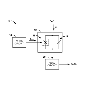
[0015] FIG. 1 illustrates an example of a Josephson magnetic memory cell
system 10
in accordance with an aspect of the invention. The Josephson magnetic memory
cell system
includes a memory cell 12 that can correspond to a single memory cell, such as
can be
included in a memory array of a random access memory (RAM). The memory cell 12
includes a Josephson junction 14 and a hysteretic magnetic Josephson junction
(HMJJ) 16
arranged in parallel, such that the Josephson junction 14 and the HMJJ 16 are
cooperatively
arranged as a superconducting quantum interference device (SQUID). It is to be
understood
that the Josephson junction 14 may also be configured as an HMJJ, and may
either be in a
static state or may participate together with HMJJ 16 in the storage of a
binary value, as
described herein.
[0016] As an example, the HMJJ 16 can include at least one fixed magnetic
material
layer and at least one free magnetic material layer having a bi-stable
orientation. At least one
of the fixed and free magnetic material layers of the HMJJ 16 can include a
magnetic polarity
that is substantially orthogonal to the magnetic polarity of the remaining
layers. As described
in greater detail herein, the substantially orthogonal magnetic polarity can
be configured to
convert superconducting Cooper pairs associated with a read current 'RD from a
singlet-state
to a triplet-state during a read operation. As a result, the logic-state
stored in the HMJJ 16
can be better distinguished during the read operation, and the HMJJ 16 can be
substantially
insensitive to manufacturing tolerances.
4
CA 02874551 2014-11-21
WO 2013/180946 PCT/US2013/040950
[0017] For example, the HMJJ 16 can be configured to store a binary value
(e.g., a
logicl or a logic-0) based on a magnetic polarization of at least one of the
free magnetic
material layers. In the example of FIG. 1, the Josephson magnetic memory cell
system 10
includes a write circuit 18 configured to generate at least one write current
IwRT on a write-
line that is magnetically coupled to the HMJJ 16. The write current(s) IwRT
can generate a
magnetic field to set the binary value of the HMJJ 16 to a binary logic-1 or a
binary logic-0
based on respective directions of current flow during a data write operation.
As an example,
the write circuit 18 can be part of a peripheral write circuit for an entire
array of memory cells
that includes the Josephson magnetic memory cell system 10.
[0018] The binary value that is stored in the HMJJ 16 can be read from
the Josephson
magnetic memory cell system 10 during a read operation in response to a read
current IRD.
As an example, the read current 'RD can correspond to a bit read current that
is applied to an
entire column of memory cells in the array, or can be individually generated
for the
Josephson magnetic memory cell system 10. The read current 'RD is provided to
Josephson
junction 14 and the HMJJ 16 at a magnitude that corresponds to the respective
critical
currents of the Josephson junction 14 and the HMJJ 16. For example, the
Josephson junction
14 can have a critical current (Ic2) that is static and the HMJJ 16 can have a
critical current
(Ici) that varies based on the orientation of the magnetic polarity of the at
least one free
magnetic material layer, and thus based on the binary value that is stored
therein. For
example, the HMJJ 16 can be configured to have a critical current having a
given magnitude
when storing a logic-0 as the binary value and can have a critical current of
approximately the
same magnitude but opposite direction when storing a logic-1. The HMJJ 16 can
thus be
configured as a "0-junction" when storing a first logic-state as the binary
value and as a "pi-
junction" when storing the second logic-state as the binary value. Therefore,
in response to
the read current 'RD, the Josephson junction 14 and the HMJJ 16 can trigger a
voltage pulse
based on their respective critical currents which can result in a total
critical current of the
memory cell 12 that is approximately equal to Ic2+Ici when storing a first
state of the binary
value and approximately equal to Ic2-Ic1 when storing a second state of the
binary value. The
difference in the response of the HMJJ 16 between the first and second logic-
states of the
stored binary value can result in variation of the magnetic flux between the
Josephson
CA 02874551 2014-11-21
WO 2013/180946 PCT/US2013/040950
junction 14 and the HMJJ 16. Accordingly, the magnetic flux between the
Josephson
junction 14 and the HMJJ 16 can be indicative of the binary value stored in
the HMJJ 16.
[0019] In the example of FIG. 1, the Josephson magnetic memory cell
system 10
includes a read circuit 20. The read circuit 20 is configured to determine the
binary value that
is stored in the HMJJ 16 in response to the read current IRD, demonstrated in
the example of
FIG. 1 as a signal DATA corresponding to the stored binary value. The read
circuit 20 can
determine the binary value in any of a variety of ways, such as based on
sensing current
magnitude, voltage pulses, or the magnetic flux between the Josephson junction
14 and the
HMJJ 16. For example, the read circuit 20 can be configured to generate a
peripheral current
through an inductor (not shown) that is magnetically coupled to the memory
cell 12, such that
the magnitude of the peripheral current changes based on the magnetic flux
between the
Josephson junction 14 and the HMJJ 16, thus indicating the binary value stored
in the HMJJ
16. Thus, while it is demonstrated in the example of FIG. 1 that the read
circuit 20 is
conductively coupled to the memory cell 12, it is to be understood that the
read circuit 20 can
instead be coupled to the memory cell 12 in a variety of different ways.
[0020] As described previously, the HMJJ 16 includes at least one fixed
magnetic
material layer and at least one free magnetic material layer having a bi-
stable orientation, and
that at least one of the fixed and free magnetic material layers of the HMJJ
16 can include a
magnetic polarity that is substantially orthogonal to the magnetic polarity of
the remaining
layers. The arrangement of the HMJJ 16 can be formed in a variety of different
ways.
[0021] FIG. 2 illustrates an example of an HMJJ 50 in accordance with an
aspect of
the invention. The HMJJ 50 can correspond to the HMJJ 16 in the example of
FIG. 1.
Therefore, reference is to be made to the example of FIG. 1 in the following
description of
the example of FIG. 2. The HMJJ 50 includes a first superconducting electrode
layer 52 and
a second superconducting electrode 54, demonstrated in the example of FIG. 2
as "S". For
example, the first and second superconducting electrode layers 52 and 54 can
be formed from
a variety of superconducting materials, such as Niobium (Nb). The first and
second
superconducting electrode layers 52 and 54 can be directly coupled to an
associated bit-read
line on which the read current IRD flows, such that the bit-read lines can
likewise be formed
from the superconducting material. The HMJJ 50 also includes a first magnetic
layer 56 and
a second magnetic layer 58, demonstrated in the example of FIG. 2 as "F", that
are separated
6
CA 02874551 2014-11-21
WO 2013/180946 PCT/US2013/040950
by a tunnel barrier layer 60. The first and second magnetic layers 56 and 58
can be fixed
magnetic layers, such that they have a substantially fixed magnetic polarity
that can be anti-
parallel with respect to each other. As an example, the first and second
magnetic layers 56
and 58 can be formed from a ferromagnetic material, such as cobalt (Co) or
iron (Fe), or a
synthetic antiferromagnetic (SAF) material. The tunnel barrier 60 is
configured to provide a
desired magnitude of the Josephson critical current through the HMJJ 50.
[0022] The HMJJ 50 further includes a first polarizing layer 62 that
interconnects the
first superconducting electrode layer 52 and the first magnetic layer 56, and
a second
polarizing layer 64 that interconnects the second superconducting electrode
layer 54 and the
second magnetic layer 58. In the example of FIG. 2, the first and second
polarizing layers 62
and 64 are demonstrated as "X" and "X", respectively. The first and second
polarizing layers
62 and 64 can be formed from a ferromagnetic material or alloy, such as nickel
(Ni),
Permalloy, palladium-nickel (PdNi), copper-nickel (CuNi), cobalt-platinum
(CoPt), or any of
a variety of other materials. At least one of the first and second polarizing
layers 62 and 64
can have a magnetic polarity that is substantially orthogonal with respect to
the magnetic
polarity associated with the first and second magnetic layers 56 and 58. In
the example of
FIG. 2, the first polarizing layer (i.e., X) is a fixed magnetic material
layer, but the second
polarizing layer 64 (i.e., X') can be a free magnetic material layer, such
that the free magnetic
material layer has a bi-stable orientation that permits a variable magnetic
polarity therein.
Therefore, the magnetic polarity of the free magnetic material layer can be
set as a result of
magnetic fields generated locally by orthogonal electrical currents, such as
the at least one
write current IwRT. Such magnetic polarity can affect the magnitude and/or
sign of the
critical current of the HMJJ 50, as described previously. Accordingly, the
binary value can
be stored in the HMJJ 50 based on the magnetic polarity of the free magnetic
material of one
of the first and second polarizing layers 62 and 64.
[0023] As a result of the substantially orthogonal magnetic polarity of
at least one of
the first and second polarizing layers 62 and 64, the angular momentum of
superconducting
Cooper pairs of a tunneling current flowing through the HMJJ 50 (e.g., the
read current IRD)
can be manipulated to convert the superconducting Cooper pairs from a singlet-
state (spin-
up/spin-down) to a triplet-state (spin-up/spin-up or spin-down/spin-down). The
conversion
of the superconducting pairs from the singlet-state to the triplet-state can
be achieved with
7
CA 02874551 2014-11-21
WO 2013/180946 PCT/US2013/040950
maximum effect based on both of the first and second polarizing layers 62 and
64 having a
substantially orthogonal magnetic polarity relative to the magnetic polarity
of the first and
second magnetic layers 56 and 58.
[0024] As a result of the conversion of the superconducting pairs from
the singlet-
state to the triplet-state, the HMJJ 50 can exhibit a number of advantages
over typical
superconductor-based memory cells, such as those that implement singlet-state
tunneling
currents for readout. For example, the triplet-state tunneling current (e.g.,
the read current
IRD) flowing through the HMJJ 50 can have a substantially greater magnitude
than a singlet-
state tunneling current, particularly when the thickness of the magnetic
layers 56 and 58 is
greater than a few nanometers. Therefore, the readout of the binary value can
be
substantially improved based on improved readout contrast between the logic-
states of the
binary value stored in the HMJJ 50, and the thickness of the magnetic layers
56, 58, 62, and
64 can be greater than typical superconductor-based memory cells. As another
example, the
magnitude of the triplet-state current can be substantially insensitive to
small variations in the
thickness of the magnetic layers 56, 58, 62, and 64. Therefore, variations of
the thicknesses
of the magnetic layers 56, 58, 62, and 64 due to fabrication tolerances during
manufacture of
the Josephson magnetic memory cell system 10 can be substantially irrelevant
to the readout
of the HMJJ 50. As another example, the spin-up/spin-up or spin-down/spin-down
electron-
pair orientation of the triplet-state can result in the triplet-state
tunneling current being
substantially sensitive to majority/minority band effects that can give rise
to tunneling
magnetoresistance (TMR) effect, which is substantially absent for singlet-
state tunneling
current that contains equal numbers of spin-up and spin-down electrons and
which
substantially concurrently samples both majority and minority bands.
Accordingly, the HMJJ
50 can be configured as a "toggle-MRAM" having significantly enhanced write
margins.
[0025] FIG. 3 illustrates an example of a diagram 100 of two states of
the HMJJ 50 in
accordance with an aspect of the invention. The diagram 100 includes a first
state 102
corresponding to a first logic-state of the binary value stored in the HMJJ 50
and a second
state 104 corresponding to a second logic-state of the binary value stored in
the HMJJ 50. It
is to be understood that the specific logic-states associated with the first
and second states
102 and 104 can be arbitrary depending on the associated readout system. The
diagram 100
8
CA 02874551 2014-11-21
WO 2013/180946 PCT/US2013/040950
demonstrates magnetic polarities in the magnetic layers 56, 58, 62, and 64
based on a
Cartesian coordinate system 106.
[0026] In the first state 102, the first magnetic layer 56 has a first
magnetic polarity in
the +X direction and the second magnetic layer 58 has a second magnetic
polarity in the ¨X
direction, and which is thus substantially anti-parallel with respect to the
first magnetic
polarity. In addition, the first polarizing layer 62 and the second polarizing
layer 64 have
magnetic polarities in the +Y direction, and which are thus parallel with
respect to each other
and substantially orthogonal to the first and second magnetic polarities. It
is to be understood
that, while the magnetic polarities of the first and second polarizing layers
62 and 64 are
demonstrated in the +Y direction, it is to be understood that the polarities
of the first and
second polarizing layers 62 and 64 could instead both be in the ¨Y direction,
the +Z
direction, or the ¨Z direction, such that they are substantially orthogonal to
the first and
second magnetic polarities. As described previously, the first polarizing
layer 62 is a fixed
magnetic material, such that the magnetic polarity is static. However, the
second polarizing
layer 64 can be a free magnetic material layer, such that the magnetic
polarity of the second
polarizing layer 64 can be set to the orientation in the first state 102 based
on at least one
write current (e.g., the write current IwRT).
[0027] In the second state 104, the magnetic polarities of the first and
second
magnetic layers 56 and 58 and the first polarizing layer 62 remain the same as
in the first
state 102, based on the first and second magnetic layers 56 and 58 and the
first polarizing
layer 62 being formed as fixed magnet material layers. However, in the second
state 104, the
second polarizing layer 64 has a magnetic polarity in the ¨Y direction, which
is thus anti-
parallel with respect to the magnetic polarity of the first polarizing layer
62 and remains
substantially orthogonal to the first and second magnetic polarities.
Therefore, in the second
state 104, the magnetic polarity of the second polarizing layer 64 is set to
the opposite
orientation as that in the first state 102 based on at least one write current
(e.g., the write
current IwRT) to change the sign of the critical current of the HMJJ 50.
Accordingly, the
magnetic polarity of the second polarizing layer 64 can dictate the binary
value that is stored
in the HMJJ 50.
[0028] FIG. 4 illustrates another example of a diagram 150 of two states
of the HMJJ
50 in accordance with an aspect of the invention. The diagram 150 includes a
first state 152
9
CA 02874551 2014-11-21
WO 2013/180946 PCT/US2013/040950
corresponding to a first logic-state of the binary value stored in the HMJJ 50
and a second
state 154 corresponding to a second logic-state of the binary value stored in
the HMJJ 50.
Similar to as described previously in the example of FIG. 2, it is to be
understood that the
specific logic-states associated with the first and second states 152 and 154
can be arbitrary
depending on the associated readout system. The diagram 150 demonstrates
magnetic
polarities in the magnetic layers 56, 58, 62, and 64 based on a Cartesian
coordinate system
156.
[0029] In the first state 152, the first magnetic layer 56 has a first
magnetic polarity in
the +X direction and the second magnetic layer 58 has a second magnetic
polarity in the ¨X
direction, and which is thus substantially anti-parallel with respect to the
first magnetic
polarity. In addition, the first polarizing layer 62 has a magnetic polarity
in the +Y direction
which is thus substantially orthogonal to the first and second magnetic
polarities, and the
second polarizing layer 64 has a magnetic polarity in the +X direction, which
is substantially
parallel with the first magnetic polarity. As described previously, the first
polarizing layer 62
is a fixed magnetic material, such that the magnetic polarity is static.
However, the second
polarizing layer 64 can be a free magnetic material layer, such that the
magnetic polarity of
the second polarizing layer 64 can be set to the orientation in the first
state 152 based on at
least one write current (e.g., the write current IwRT)=
[0030] In the second state 154, the magnetic polarities of the first and
second
magnetic layers 56 and 58 and the first polarizing layer 62 remain the same
based on the first
and second magnetic layers 56 and 58 and the first polarizing layer 62 being
formed as fixed
magnet material layers. However, in the second state 154, the second
polarizing layer 64 has
a magnetic polarity in the ¨Y direction, which is thus anti-parallel with
respect to the
magnetic polarity of the first polarizing layer 62 and is substantially
orthogonal to the first
and second magnetic polarities. Therefore, in the second state 154, the
magnetic polarity of
the second polarizing layer 64 is rotated substantially 90 relative to the
first state 152 based
on at least one write current (e.g., the write current IwRT)=
[0031] For example, the second polarizing layer 64 can be formed from a
magnetic
material having a bi-axial anisotropy, such that the magnetic polarity can be
set orthogonally
on easy axes with respect to the first and second states 152 and 154. For
example, the
magnetic polarities of the second polarizing layer 64 in each of the first and
second states 152
CA 02874551 2014-11-21
WO 2013/180946 PCT/US2013/040950
and 154 can be set based on a relative magnitude of two write currents IwRT to
adjust a
magnetic polarity vector in the second polarizing layer 64. As described
previously, the
conversion of the superconducting pairs from the singlet-state to the triplet-
state can be
achieved with maximum effect based on both of the first and second polarizing
layers 62 and
64 having a substantially orthogonal magnetic polarity relative to the
magnetic polarity of the
first and second magnetic layers 56 and 58. Therefore, in the first state 152,
the HMJJ 50 can
exhibit substantially diminished conversion of the superconducting pairs to
the triplet-state.
As a result, the HMJJ 50 in the example of FIG. 4 can be fabricated in a
manner that the
thickness of the magnetic layers 56 and 58 can be sufficient to substantially
prevent a
predominantly singlet-state tunneling current from flowing through the HMJJ 50
in the first
state 152. In the second state 154, with both of the first and second
polarizing layers 62 and
64 being substantially orthogonal to the first and second magnetic polarities,
and thus having
maximum conversion of the superconducting pairs to the triplet-state, the
predominantly
triplet-state tunneling current can flow through HMJJ 50. Accordingly, the
binary value that
is stored in the HMJJ 50 in the example of FIG. 4 can be read from the HMJJ 50
based on
whether the tunneling current (i.e., the read current IRD) flows through the
HMJJ 50.
[0032] It is to be understood that the HMJJ 50 is not intended to be
limited to the
example of FIGS. 2-4. For example, the layers of the HMJJ 50 need not be
formed in the
specific order and orientation demonstrated in the example of FIG. 2. For
example, the
location of the tunnel barrier 60 relative to the magnetic layers 56, 58, 62,
and 64 can be
substantially interchangeable. Additionally, while the magnetic layers 56, 58,
62, and 64 and
the superconducting electrode layers 52 and 54 are demonstrated as having
substantially
equal thickness, the thicknesses of the layers can vary relative to each
other. In addition, the
magnetic layers 56, 58, 62, and 64 may be formed with different magnetic
materials. Also,
the orientations of the magnetic polarities are not limited to the specific
orientations provided
in the examples of FIGS. 2-4, but could instead have corresponding anti-
parallel or
orthogonal magnetic polarities, as described previously. As a further example,
the magnetic
layers 56 and 58 in FIGS. 2-4 may be replaced with a single magnetic layer
having a single
fixed magnetic polarity, such that the tunnel barrier 60 is arranged directly
above or below
the single magnetic layer. For example, in FIG.2, the magnetic layers 56 and
58 can be
replaced with a single magnetic layer having perpendicular magnetic anisotropy
with its
11
CA 02874551 2014-11-21
WO 2013/180946 PCT/US2013/040950
magnetic polarity being fixed in approximately the +Y direction, whereas the
magnetic
polarities of the respective fixed and free polarizing layers 62 and 64 can be
oriented in the
X- or Z-axes. Furthermore, as described in the example of FIG. 5, an HMJJ
could include
additional magnetic layers.
[0033] FIG. 5 illustrates an example of an HMJJ 200 in accordance with an
aspect of
the invention. The HMJJ 200 can likewise correspond to the HMJJ 16 in the
example of FIG.
1. Therefore, reference is to be made to the example of FIG. 1 in the
following description of
the example of FIG. 5. The HMJJ 200 includes a first superconducting electrode
layer 202
and a second superconducting electrode 204, demonstrated in the example of
FIG. 5 as "S".
The HMJJ 200 also includes a first magnetic layer 206 and a second magnetic
layer 208,
demonstrated in the example of FIG. 5 as "F". The first and second magnetic
layers 206 and
208 can be configured as SAF layers having a fixed magnetization, such that
they have a
substantially fixed magnetic polarity that can be anti-parallel with respect
to each other. The
HMJJ 200 also includes a third magnetic layer 210 and a fourth magnetic layer
212,
demonstrated in the example of FIG. 5 as "F" that are similarly as SAF layers
such that their
magnetization is substantially anti-parallel with respect to each other. As an
example, while
the magnetic layers 206 and 208 and the layers 210 and 212 are demonstrated in
an SAF
configuration, it is to be understood that at least one of the pairs of
magnetic layers 206 and
208 and magnetic layers 210 and 212 can be alternatively replaced with a
single
ferromagnetic layer. The first magnetic layer 206 and the fourth magnetic
layer 212 are
separated by a tunnel barrier 214.
[0034] The third and fourth magnetic layers 210 and 212 can be configured
as a free
SAF, such that the magnetization of the third and fourth magnetic layers 210
and 212 is anti-
parallel with respect to each other along an axis that has a bi-stable
orientation, such as to
permit a variable magnetic polarity therein. Therefore, the magnetic polarity
of the third and
fourth magnetic material layers 210 and 212 can be set as a result of magnetic
fields
generated locally by orthogonal electrical currents, such as the at least one
write current IwRT.
Such magnetic polarity can affect the magnitude of the critical current of the
HMJJ 200, as
described previously. Accordingly, the binary value can be stored in the HMJJ
200 based on
the magnetic polarity of the third and fourth magnetic material layers 210 and
212.
12
CA 02874551 2014-11-21
WO 2013/180946 PCT/US2013/040950
[0035] The HMJJ 200 further includes a first polarizing layer 216 that
interconnects
the first superconducting electrode layer 202 and the third magnetic layer 210
and a second
polarizing layer 218 that interconnects the second superconducting electrode
layer 204 and
the second magnetic layer 208. In the example of FIG. 5, the first and second
polarizing
layers 216 and 218 are demonstrated as "X". The first and second polarizing
layers 216 and
218 can be formed from a ferromagnetic material or alloy with magnetization
lying in a plane
of the device or perpendicular to the device, similar to as described
previously in the example
of FIG. 2. As another example, the first and second polarizing layers 216 and
218 can be
formed from magnetic materials having a conical magnetization, such as holmium
(Ho), or
can be arranged as surface-pinned domain walls. The first and second
polarizing layers 216
and 218 can have a magnetic polarity that is substantially orthogonal with
respect to the
magnetic polarity associated with the magnetic layers 206, 208, 210, and 212,
or otherwise
provide a magnetization having an orientation that is inhomogeneous throughout
the first and
second polarizing layers 216 and 218. Accordingly, the first and second
polarizing layers
216 and 218 can be configured to convert the superconducting Cooper pairs
associated with
the tunneling current (i.e., the read current IRD) from the singlet-state to
the triplet-state. In
the example of FIG. 5, the first and second polarizing layers are fixed
magnetic material
layers.
[0036] As described above, superconducting Cooper pairs that are in a
triplet-state
can be essentially spin-polarized. As a result, the triplet-tunneling matrix
element across the
tunnel barrier 214 can be sensitive to a relative alignment of the first and
fourth magnetic
layers 206 and 212. This can be akin to the tunneling magnetoresistive (TMR)
effect that is
used in MRAM devices. However, in the case of the HMJJ 200, it is the
magnitude of the
Josephson critical current that is affected by the relative alignment of
magnetic layers 206
and 212 rather than the resistance of the Josephson junction. This effect is
absent in the
tunneling of singlet-state superconducting Cooper pairs, and is enabled in
HMJJ 200 by the
incorporation of the polarizing layers 216 and 218.
[0037] FIG. 6 illustrates an example of a diagram 250 of two states of
the HMJJ 200
in accordance with an aspect of the invention. The diagram 250 includes a
first state 252
corresponding to a first logic-state of the binary value stored in the HMJJ
200 and a second
state 254 corresponding to a second logic-state of the binary value stored in
the HMJJ 200. It
13
CA 02874551 2014-11-21
WO 2013/180946 PCT/US2013/040950
is to be understood that the specific logic-states associated with the first
and second states
252 and 254 can be arbitrary depending on the associated readout system. The
diagram 250
demonstrates magnetic polarities in the magnetic layers 206, 208, 210, 212,
216, and 218
based on a Cartesian coordinate system 256.
[0038] In the first state 252, the first magnetic layer 206 has a first
magnetic polarity
in the +X direction and the second magnetic layer 208 has a second magnetic
polarity in the ¨
X direction, and which is thus substantially anti-parallel with respect to the
first magnetic
polarity. In addition, the third magnetic layer 210 has the first magnetic
polarity and the
fourth magnetic layer 212 likewise has the second magnetic polarity, thus
forming a
substantially anti-parallel alignment of the fourth magnetic layer 212 and the
first magnetic
layer 206 on the opposite sides of the tunnel barrier 214. Furthermore, the
first polarizing
layer 216 and the second polarizing layer 218 have magnetic polarities in the
+Y direction,
and which are thus parallel with respect to each other and substantially
orthogonal to the first
and second magnetic polarities. It is to be understood that, while the
magnetic polarities of
the first and second polarizing layers 216 and 218 are demonstrated in the +Y
direction, it is
to be understood that the polarities of the first and second polarizing layers
216 and 218 could
instead both be in the ¨Y direction, the +Z direction, or the ¨Z direction,
such that they are
substantially orthogonal to the first and second magnetic polarities. In
addition, as stated
previously, the polarizing layers 216 and 218 may have a conical magnetization
or otherwise
affect an inhomogeneous magnetization that results in a conversion of a
significant portion of
the tunneling current to a triplet-state.
[0039] In the second state 254, the magnetic polarities of the first and
second
magnetic layers 206 and 208 and the first and second polarizing layers 216 and
218 remain
the same based on the first and second magnetic layers 206 and 208 and the
first and second
polarizing layers 216 and 218 being formed as fixed magnet material layers.
However, in the
second state 254, the third and fourth magnetic layers 210 and 212 have a
magnetic polarity
in the ¨X direction and +X direction, respectively, thus forming a
substantially parallel
alignment of the fourth magnetic layer 212 and the first magnetic layer 206 on
the opposite
sides of the tunnel barrier 214. Therefore, in the second state 254, the
magnetic polarities of
the third and fourth magnetic layers 210 and 212 are set to the opposite
orientation as that in
the first state 252 based on at least one write current (e.g., the write
current IwRT) to change
14
CA 02874551 2014-11-21
WO 2013/180946 PCT/US2013/040950
the critical current of the HMJJ 200 based on a TMR effect experienced by the
spin-polarized
triplet-state electrons of the read current 'RD. Accordingly, the magnetic
polarity of the third
and fourth magnetic layers 210 and 212 can dictate the binary value that is
stored in the
HMJJ 200.
[0040] FIG. 7 illustrates an example of a Josephson magnetic random
access memory
(JMRAM) system 300 in accordance with an aspect of the invention. The JMRAM
system
300 can be implemented as a memory structure in a variety of quantum and/or
classical
computing applications. As an example, the JMRAM system 300 can be configured
cryogenically in a quantum computing circuit, such as operating at
approximately 4 Kelvin or
less, to store classical data and/or controller instructions in a quantum
computing
environment.
[0041] The JMRAM system 300 is demonstrated in the example of FIG. 7 as
being
arranged as an array of memory cells 302. Specifically, the memory cells 302
are arranged in
rows 304 that each correspond to a data word, demonstrated as WORD 0 through
WORD Y,
where Y is an integer greater than 1. Each of the rows 304 includes a set of
memory cells
302 that form X columns 306 across the rows 304, with the memory cells 302 in
WORD 0
being demonstrated in the example of FIG. 7 as Co to Cx, where X is an integer
greater than
1. Therefore, each of the memory cells 302 in the array of the JMRAM system
300 can be
individually addressable by row 304 and column 306.
[0042] In the example of FIG. 7, each of the rows 304 is demonstrated as
having an
associated word-write line 308 and word-read line 310, demonstrated as WLW0
and WLRo
through WLWy and WLRy, respectively. The word-write line 308 and word-read
line 310
can be inductively and/or magnetically coupled to each of the memory cells 302
in each of
the rows 304 of the JMRAM system 300. In addition, each of the memory cells
302 is
demonstrated as having an associated bit-write line 312 and bit-read line 314,
demonstrated
as BLW0 and BLR0 through BLWy and BLRy, respectively. The bit-write line 312
and bit-
read line 314 can be coupled to each corresponding numbered memory cell 302 in
each of the
rows 304 of the JMRAM system 300, such that the memory cells 302 in each
column 306 are
arranged in series with respect to the bit-write line 312 and bit-read line
314.
[0043] Each of the memory cells 302 is configured to store a single bit
of data.
Specifically, each of the memory cells 302 can be configured substantially
similar to the
CA 02874551 2014-11-21
WO 2013/180946 PCT/US2013/040950
memory cell 12 in the example of FIG. 1. Specifically, each of the memory
cells 302 can
include an HMJJ, such as similar to the HMJJ 50 or 200 in the examples of
FIGS. 2 and 5,
respectively, that can be configured to store the binary value corresponding
to a binary logic-
1 or a binary logic-0. The binary value can be set in response to a word-write
current that is
provided on the respective word-write line 308 and a bit-write current that is
provided on the
respective bit-write line 312, such as to change a magnetic polarity of at
least one free
magnetic material layer. Similarly, the respective digital state that is
stored in each of the
memory cells 302 can be read from the memory cells 302 based on a word-read
current that
is provided on the respective word-read line 310 to select a given one of the
rows 304 and a
bit-read current that is provided on the respective bit-read line 314.
Specifically, the bit-read
line 314 of each of the columns 306 is coupled to a sense register 316 that is
configured to
determine whether the binary value of each of the memory cells 302 of an
associated row 304
corresponds to a binary logic-1 state or a binary logic-0 state in response to
the word-read
current and the bit-read current during a read operation. As an example, the
sense register
316 can measure a voltage or a current associated with the bit-read line 314,
or a magnetic
flux in each of the respective memory cells 302, as described in the example
of FIG. 1.
[0044] What have been described above are examples of the invention. It
is, of
course, not possible to describe every conceivable combination of components
or
methodologies for purposes of describing the invention, but one of ordinary
skill in the art
will recognize that many further combinations and permutations of the
invention are possible.
Accordingly, the invention is intended to embrace all such alterations,
modifications, and
variations that fall within the scope of this application, including the
appended claims.
16