Note: Descriptions are shown in the official language in which they were submitted.
CA 02874615 2014-11-20
WO 2013/177511 PCT/US2013/042641
HIGH POWER OPTICAL SWITCH
FIELD OF THE INVENTION
[00011 The concepts, systems, circuits and techniques described herein relate
to optical
systems and more particularly to optical switches.
GOVERNMENT RIGHTS
[00021 This invention was made with government support under Grant No. FA8650-
06-C-
7211, awarded by the United States Air Force, The government has certain
rights in this
invention.
BACKGROUND OF THE INVENTION
[0003] As is known in the art, there is a trend toward providing lasers having
power ranges
in the range of several hundred watts or greater (so-called "high power"
lasers).
[0004] As is also known, as high-power lasers move into the mainstream, there
is a
concomitant wowing need for non-mechanical means to switch (or route) high-
power
laser beams from one node to another. As one commercial example, in the laser
material
processing field it is frequently cost effective to have a single high-power
laser feed
multiple material processing stations. The only presently known means to
switch high-
power lasers are mechanical, which are costly, slow, inefficient, unreliable,
and limited in
the number of available switching ports. This is especially true if the beam
to be switched
is a single mode in a fiber delivery cable, such as used with coherent lasers.
This is due, at
least in part, to the fact that the energy must be coupled into a fiber core
that is often on
the order of 10 microns in diameter. As a further example, with increasing use
of optical
sensors on aircraft, there is an increasing need a. single laser, mounted
within the aircraft,
be capable of rapidly routing optical signals to multiple optical windows
located, around an
aircraft periphery. To date, there has been no known means to non-mechanically
switch
high-power laser beams, let alone to do it efficiently, quickly, cost
effectively, and
reliably.
CA 02874615 2014-11-20
WO 2013/177511 PCT/US2013/042641
SUMMARY OF THE INVENTION
[0005] Described herein are concepts, systems, circuits and techniques to non-
mechanically switch high power laser beams efficiently, quickly, cost
effectively and
reliably. Variations are described for both polarized and unpolarized light.
[0006] in accordance with the concepts, systems, circuits and techniques
described herein,
a switch for switching high power laser beams between locations or between
applications
includes a switchable, high-power (HP) liquid crystal (LC) half-wave plate
(HWP) oriented
with a fast axis at an angle of forty-five (45) degrees to an input
polarization direction and a
polarizing beam splitter adjusted such that the HWP acts as a polarizing
rotator.
[0007] With this particular arrangement, an optical switch which enables the
switching
of laser beams having power levels ranging from up to about 50 kW is provided.
In one
embodiment, the optical switch enables the switching of laser beams having
power levels
ranging from about 100 W to at least 10 kW.
[0008] In accordance with a further aspect of the concepts described herein,
techniques for
constructing a wide variety of non-mechanical high power switches are
provided.
[0009] Th.e novelty of at least some of the concepts, systems, circuits and
techniques
described herein lies, at least in part, within the means by which such switch
architectures
can be instantiated with novel high-power componentry, and thereby enable high-
power
switches.
[00010] A switch in accordance with the concepts, systems, circuits and
techniques
described herein is capable of swathing a minimum of I kW, and possibly ten
times
higher powers. As such, the concepts, systems and techniques described herein
offer
several ordens of magnitude improvement in power handling over the current
state-of-the-
art switches.
[0011] .A switch provided in accordance with the techniques described herein
on the other
hand, is capable of switching in less than 50 microseconds which is a full
three orders of
magnitude faster than known prior art techniques.
2
CA 02874615 2014-11-20
WO 2013/177511 PCT/US2013/042641
[0012] Polarizing beam splitting (PBS) cubes are often used to provide low-
power
optical switches. The physical position of the PBS output beam depends upon
the
polarization state of the input beam. By switching a polarization, a beam can
be switched
from one place to another. Switching a polarization is typically accomplished
with the use
of a polarization rotator.
[0013] However, until now, there have been no high-power polarization rotators
suitable
for use in such systems.
[0014] It has, however, in accordance with the concepts, systems, circuits and
techniques
described herein, been recognized that a high-power phase retarder may be
utilized as a
high-power polarization rotator. This use, in turn, enables a wide variety of
high-power
switches to be provided. In particular, by coupling such a high-power
polarization rotator
with a high-power polarizing beam splitter, a basic building block for optical
switches
which are able to switch high power laser beams is provided.
[0015] In accordance with a still further aspect of the concepts, systems,
circuits and
techniques described herein, a high-power phase retarder, implemented as a
polarization
rotator is used to enable operation of switch architectures which were
heretofore only
suitable for use at relatively low power levels.) at power levels two to three
orders of
magnitude higher than has been previously possible.
BRIEF DESCRIPTION OF THE DRAWINGS
[0016] Fig. 1 is a block diagram of an optical switch having an input port and
a pair of
output ports (a lx2 switch).
[0017] Fig. 2 is a block diagram of a 1x2 high-power switch for coupling into
fibers.
[0018] Fig. 3 is a block diagram of a I xM high-power switch comprising M
building
blocks from Fig. 2
[0019} Fig. 4 is a block diagram of a 2x2 Optical Cross Connect Switch.
[0020] Fig. 5 is a block diagram of a block diagram of non-blocking 2x2 Cross-
connect
Switch.
3
CA 02874615 2014-11-20
WO 2013/177511 PCT/US2013/042641
[0021] Figs. 6A--- 6C are block diak.gains of switches capable of use with
.unpolarized
light.
[0022] Fig. 7 is a block diagram of a Nx2 router capable of coupling light
from
unpolarized laser diode pumps to multiple arrays.
[0023] Fig. 8 is a block diagram of which illustrates a operation of a
polarizing beam
splitter cube.
[002.4] Fig. 9 is a block diagram of a liquid crystal (LC) phase retarder.
DETAILED DESCRIPTION OF THE. PREFERRED EMBODIMENTS
[0025] Referring now to Fig. 1, a switch 10 having an input 12 and a pair of
outputs 14, 16
includes a switehable high-power (RP) liquid crystal (LC) half-wave plate
(HWP) 18
disposed at the input 12 and a polarizing beam splitter (PBS) disposed.
adjacent the HWP 12.
[0026] It should he appreciated that switch 10 corresponds to a single input-
two output
switch (i.e, a lx2 switch). Thus, switch 10 is capable of routing a high-power
beam
incident at the single input port 12 to either of the two output ports 14, 16.
[0027] in operation, an incident polarized laser beam (designated. with
reference numeral
22 in Fig. 1) is passed through a switchable high-power (HP) liquid crystal
(LC) half-wave
plate (HWP), oriented with its fast axis at 450 to the input polarization
direction and
subsequently through polarizing beam splitter (PBS) 20. When so adjusted, the
HWP acts
as a polarization rotator.
[0028] It should be appreciated that although beams 22., 24, 26 are here
illustrated as
free-space beams; those of ordinary skill in the art will appreciate that any
or all of beams
22, 24, 26 could equally well be provided as a beam from a fiber laser (e.g.
an expanded,
collimated beam from a fiber laser).
[0029] The HWP in its "off" state converts an optical signal having a. first
polarization
(designated as "p" polarization in Fig. 1) to a second polarization
(designated as "s"
polarization in Fig. I). In its "on" state, the MVP is a null polarization
operator (i.e. no
polarization change is affected by the MVP). The nomenclature of "off" and
"on" refers
to the preened embodiment of the MVP as a LCHWP, which becomes a null operator
4
CA 02874615 2014-11-20
WO 2013/177511 PCT/US2013/042641
when voltage is applied but a fixed-orientation HWP when the voltage is off or
at least
much lower.
[0030] It should also be appreciated that in the exemplary embodiment of Fig.
1, the PBS
is shown as a beam splitting cube. Those of ordinary skill in the art will
appreciate that
the PBS could equally be provided as an optical window coated with an
appropriate
dielectric thin film (an arrangement known as a polarizing plate with the
plate oriented at
the proper angle to effect the same polarization discrimination as a PBS).
[0031] A PBS nominally passes light having a first polarization (e.g. the p
polarized light
in Fig. 1) and reflects (here downward) light having a second polarization
(e.g. the s
polarized light in Fig. 1). The HWP and PBS form a switching stage and when
the HWP
is on, p polarized input light is passed through this switching stage to the
first output port.
When the HWP is off the input p polarized light is converted to s and
reflected downward
to the second output port.
[0032] In Fig. 1 the light entering and exiting each port is shown as a
collimated free-
space beam; however, for many high-power applications it is preferable to
couple the
output light to and from a fiber.
[0033] Referring now to Fig. 2, in which like elements of Fig. I are provided
having like
reference designations, a high power switch providing light signals to optical
fibers 38,40
further includes a pair of optical phased arrays arranged as a tip/tilt/focus
subsystem
(ITFOPA) (i.e. two OPAs with their steering axes in different directions,
preferably
approximately perpendicular) provided at each port 14, 16 and lenses 30, 32
disposed to
nominally focus output beams 24, 26 for matching of a fiber mode to respective
ones of
the optical fibers 38, 40.
[0034] The TITOPA disposed at each port provides for very fine angular
(azimuth and
elevation) and very fine focus adjustments to match the fiber mode to a
relatively high
accuracy. Instead of having a TTFOPA at each output port, a single TITOPA
located
upstream (in the common path) may be uses, as will be obvious to one of skill
in the art.
Furthermore, if the input beams may have significant positional variability as
well as
CA 02874615 2014-11-20
WO 2013/177511 PCT/US2013/042641
angular variability, a pair of TITOPAs, separated by some propagation
distance, may be
used, to adjust both position and angle of the beams for optimum fiber
coupling.
[0035] Re-coupling light back into a fiber is a notoriously sensitive process;
the focussed
spot must be within a few microns of the desired longitudinal position and a
fraction of a
micron of the desired transverse position to couple efficiently to the fiber
mode. For a
typical focal length of the coupling lens of some tens of mm, the required
angular
settability of the TTFOPA is of the order of 10 grad. To ensure this, a
control loop circuit
42 (or more simply control circuit 42) is coupled between the output optical
fiber 40 and
the TITOPA 32.
[0036] Control circuit 42 samples the power level in the output fiber 40 via
coupler 44
and provides the sampled signal to a processor which in turn provides signals
to TITOFA
to adjust the two ITFOPA angles and fbcal powers in two dimensions for maximum
power coupled into fiber 40. It should be appreciated that a similar control
circuit can be
provided at each additional output port,
[0037] In the exemplary embodiment of Fig. 2, control circuit 42 comprises a
coupler 44
(here shown as a. directional coupler) 44, a processor 46 and a signal path
48. Coupler 44
couples a portion of light signals propagating in optical fiber 40 to an input
of processor
46 and signal path 48 couples signals from an output of processor 46 to TTFOPA
32,
Thus, in this exemplary embodiment, coupler 44 couples a portion of the light
signal
propagating in the output fiber 40 to an SPCID processor which performs a
stochastic
parallel gradient descent (SPUD) process on the signals provided thereto. SPUD
processor then. provides signals along signal path 46 to `ITFOPA to adjust the
two
rimp.A. angles and focal powers in two dimensions for maximum power coupled
into
fiber 40. A similar circuit can be at each additional output port.
[0038] It should be appreciated that the combinations of FIWP 18 and PBS 20
shown in
Figs. I and 2 comprise basic building blocks for switching fabrics, the
cascading of which
enables the creation of many other complex switching fabrics.
6
CA 02874615 2014-11-20
WO 2013/177511 PCT/US2013/042641
[00391 It should of course be appreciated that embodiments may include a
single
TITOPA, upstream of the HWP while other embodiments may include two 'ITFOPAs,
either both upstream, both downstream, or one each.
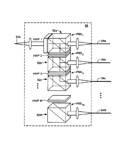
[0040] Referring now to Fig. 3 in which like elements of Figs. 1 and 2 are
provided
having like reference designations, a switch 50 is provided from a plurality
of, here M,
switch stages 52a 52M, generally denoted 52. Switch 50 has an input 53a and a
plurality
of outputs 54a-54M and thus switch 50 is provided as a 1 X M switch.
[0041} In this exemplary embodiment, each switch stage 52 is comprised of a 1
x 2
switch element 10 (also sometimes referred to herein as elementary building
blocks 10 or
more simply building blocks 10). Thus, switch 50 is provided from a plurality
of, here M.
1 x 2 switch elements 10 which may be the same as or similar to switch
elements 10
described above in conjunction with Figs. 1 and 2.
[0042] It should be noted that switch elements 10 are coupled to provide the 1
X M
switch 50. Switch 50 is capable of routing an optical signal provided to input
500 to any
of output ports 54a ¨ 54M (i.e. M different output ports). It Should be
appreciated that in
the exemplary embodiment of Fig. 3, an example of switching between high-power
optical
fibers is Shown, however, it should be understood that switch 50 is also
capable of
switching free space beams.
[0043) Operation of switch 50 can be explained as follows. Assume p polarized
light is
provided from a laser (not shown in Fig. 3) to switch input 53a and coupled to
switch a
first switch stage 52a. When ITWP1 of stage 52a is son' its retardance is zero
and the light
remains p polarized and passes straight through PI351 to a first output port
54a. When
IMP! is 'off its retardance is 180'? and the polarization is transformed to s
upon passage
through HWPj, and the beam is consequently reflected downward from PBSI and
into the
second switching stage 52b.
[00441 If HWP2in switch stage 52b is off, the light remains s polarized and
reflects from
PBS, and exits port 54b. If IIWP2 is 'on' the light is transformed to p
polarization and
passes through P1352 into the third switching stage 52c, and so on. In this
way M
7
CA 02874615 2014-11-20
WO 2013/177511 PCT/US2013/042641
switching stages allow the light to be routed to any of M ports. Such a IxM
switch is
required if it is desired to route a centrally located high-Nwer laser to
multiple apertures
distributed about the periphery of an aircraft. Som embodiments include an
optional
TrFORA located upstream of the input near HWP1 or downstream of the outputs
(just
upstream of the focussing lens), as described above in conjunction with Fig.
2. Thus, it
should be appreciated that embodiments may include a single TTFOPA, upstream
of the
HWP while other embodiments may include two Fl FOP.As, either both upstream,
both
downstream, or one each.
[0045] in view of the above and as will become further apparent from the
description
herein below, it should now be appreciated that a variety of optical
components, such as
cross-connect switches for example, can also be constructed from multiple
units of the
basic building block of Fig. I.
100461 Referring now to Fig. 4, a cross connect switch is described. It should
be noted
that to promote clarity in the drawings and text a 2 x 2 cross connect 60 is
described, but
those of ordinary skill in the art will, after reading the description
provided herein,
appreciate that the same concepts may be applied to provide all NXN cross
connect switch.
Turning now to Fig. 4, the 2 x 2 cross connect 60 is provided if the input of
a first i x2
switch 50', which may be the same as or similar to the type shown in Fig. S.
is connected
to port 1' and a. second I xM switch 50" of the same type is connected to port
2', a 2xM
switch results. Such a switch can be used to implement redundancy.
[00471 in operation, port' can be connected to either port 1' or port 2', and
port 2 can
likewise be connected to either of ports 1' and 2'. With H\IVPi on and HWP3
both 'on', a
p-polarized beam at port I is transmitted straight through to port. 1'. With
11W131 and
IIWP2 both 'on' and H WP4 'off', a p-polarized beam at port 1 is transmitted
to port. 2' via
two reflections and a transmission through PBS cubes I, 2, and 4. Switching
from port 2
is accomplished similarly.
[0048] In one exemplary use, a primary high-power laser connected. to port I
can be
routed to any of the M ports of the lxM switch 50'. Should the primary laser
fail, a.
backup high-power laser connected to port 2 of switch 50" can then be pouted
to any of the
8
CA 02874615 2014-11-20
WO 2013/177511
PCIYUS2013/042641
same M ports of the 1xM swath. This is a so-calle41 blocking switch: one can
switch
either port 1 or port 2 to port 1' or port 2', but not both simultaneously.
00491 Referring now to Fig. 5, a switch 70 having a so-called. "non-blocking"
switching
architecture includes a first PBS 72, a HWP 74 and a second PBS 76 disposed in
an
optical path. PBSs 72, 76 and HWP 74 may be the same as or similar to PBS's
and HWPs
discussed above in conjunction with Figs. 1-4. Switch 70 allows simultaneous
switching
of port I and port. 2,
[0050] In operation, port I can be connected to either port.' or port 2', and
port 2 can
likewise be connected to either of ports 1 ' and 2'. In particular, with MVP
74 off', a p-
polarimi beam at port I is transmitted straight through to port 1' and
likewise an s-
polarized beam at port 2 is reflected twice and transmitted thereby to port
2'. With IMP
74 'on' a pi-polarized beam at port I is transmitted through PBS 72 and MVP 74
and
reflected to port 2' as an s polarized beam via PBS 76. Likewise, the s
polarized, input at
Port 2 is changed to p polarization and is transmitted to port P. Accordingly,
a first input
laser beam having a p polarization and designated with reference numeral 77 in
Fig. 5 can
be coupled to either of switch port P or switch port 2' through switch 70 by
properly
biasing HWP 74 to its on or off states.
[0051] Switching from port 2 is accomplished similarly. That is, with IMP 74
off, an
s-polarized beam at port 2 is first reflected via PBS 72 through HWP 74 to PBS
76. PBS
76 which reflects the s polarized beam to port 2'. With HWP 74 'on' an s-
polarized beam
at port 2 is reflected through PBS 72 to HWP 74 and is transmitted straight
through PBS
76 to port V. Accordingly, a second input laser beam having a s polarization
and
designated with reference numeral 78 in Fig. 5 can be coupled to either of
switch port l'
or switch port 2' through switch 70 by properly biasing I-INWP 74 to its on or
off states.
[0052] It should be appreciated that the switches discussed above assume a
polarized
input beam. Not all beams, however, are polarized. Thus, switches tbr non-
polarized light
are described,
9
CA 02874615 2014-11-20
WO 2013/177511 PCT/US2013/042641
(00531 One important example of switches for non-polarized light is that of
laser pump
diodes. One system architecture which utilizes centralized lasers and
distributed apertures
is centralized pump diodes distributed to multiple apertures, each with an
associated gain
medium, 'Thus, there is considerable interest in being able to mute laser
diode pump
beams, which are generally not polarized,
[0054j Figs. 6,A. and 6B illustrate a 1x2 switch 80 capable of operation with
=polarized
[0055] Referring now to Fig. 6A, an =polarized input beam is split into s and
p
components at an. input port 82a of a PBS cube 82. With the FIWPs 84, 86
"off," both
signal components (i.e. both the s and p components) are routed to a first
output port 82b
(designated as "Aperture .1, Array 1" in Fig. 6A), and recombined.
[00561 Fig. 613 shows the case of both MVPs "on," in which case both of the s
and p
components are routed to a second output port 82c (designated as "Aperture J,
Array 2" in
Fig. 613) where they are recombined.
[0057] Fig. 6C shows an alternate embodiment in which when both HWPs are
"off," in
which case both of the s and p components are rooted to the second output port
82c
(designated as "Aperture 2, Array 2" in Fig. 6C) Where they are recombined.
00581 Referring now to Fig. 7, an Nx2 switch 90 for switching =polarized diode
pumps
(which are intended to he representative of any =polarized laser source) is
provided from
a plurality of switch stages 92 (hem N switch stages) each of which may be the
same as or
similar to a cascade of switches 70 described above in conjunction with the
figure which
replaces 6..
[0059] In this exemplary embodiment, a plurality of laser sources, here shown
as N
diode pumps 92, are switehed to one of first and second phased arrays 94, 96,
With no
loss of generality, in this exemplary embodiment switch 90 is arranged such
that diode
pump N is routed to the Nth aperture of either of first or second arrays, 94,
96. Those of
CA 02874615 2016-04-01
,
ordinary skill in the art will appreciate, of course, that other switch
arrangements (e.g. to
route diode pump N to other apertures) may be used
[0060] In this switch, P and S polarizations traverse different paths and
experience
different losses. Typical losses for each switch interface are listed for both
S and P
components. The largest loss involves re-coupling the light back into a fiber.
In this
example, a large-core fiber is assumed, as is usually the case for the
transport of
unpolarized, incoherent pump lasers. Coupling losses would be higher, perhaps
twice as
high, for coupling into a single mode fiber. These coupling losses are not
relevant for the
free-space version of the switch.
[0061] It should be appreciated that the polarizing beam splitters appropriate
for use as
described herein are available as high-power options of COTS components.
[0062] Referring now to Fig. 8, a polarizing beam splitter (PBS) 100 capable
of
operation as a polarizer is described. An incident beam 102 comprises
components of
both p (parallel to the plane of incidence, depicted with arrows generally
denoted 104) and
s (perpendicular to the plane of incidence, depicted with dots generally
denoted 106)
polarization. A diagonal interface 108 between the two right-angle prisms 110,
112 is
provided with a thin-film dielectric coating that allows p polarization to
pass and s
polarization to be reflected.
[0063] The types of thin-film coatings typically used limit the useful
wavelength range to
about 10% about the center design wavelength. Consequently, switches are
intended for
use at or about standard laser wavelengths. Transmission through such a PBS is
typically
> 95% for p polarization and reflection is > 99% for s polarization. Note that
the switch is
arranged such that switching to port M requires M (low loss) s reflections but
only a single
(higher loss) p transmission.
[0064] The entrance and exit faces are typically provided with high-quality
antireflection
coatings. Commercially available PBS' comprised of thin-film coated fused
silica glass
prisms, as an example, have laser damage thresholds typically of the order of
5 MW/cm2
11
CA 02874615 2016-04-01
(cw) and 10 Pcm2 (10 ns), which is more than adequate for the 1 to 50 kW (cw)
power
levels contemplated for this switch.
[0065] Alternatively, thin-film polarization plates can be used in place of
the
polarization beam splitting cubes. These have similar damage thresholds, but
offer
somewhat higher transmissions, especially for p polarization, where T> 97% is
routinely
offered for high-power versions. The use of polarization plates instead of
prisms can
reduce the amount of glass in the optical path, which is beneficial for
preservation of high
beam quality, which is needed for efficient coupling into a single-mode fiber.
[0066] The variable HWP retarder as described herein is based upon liquid
crystal (LC)
technology, and is used primarily as a two-state switch.
[0067] Referring now to Fig. 9, a phase retarder 120 comprises two transparent
substrates, each provided with transparent, conducting thin-film electrodes
and appropriate
antireflection coatings, and a liquid crystal layer of appropriate thickness
sandwiched
between the substrates. The upper portion 122 illustrating the liquid crystals
oriented such
that an incident wave 123 sees an ordinary refractive index no (the voltage
'on' state); the
lower portion 124 illustrates the liquid crystals oriented such that an
incident wave sees
the extraordinary refractive index ne (the voltage 'off' state).
[0068] The phase retardance 5 is given by ö = 2ndAna, where d is the cell
thickness, A =
ne-no is the LC birefringence, and X the wavelength.
[0069] A HWP is constructed with sufficient LC thickness to provide a minimum
of
180 retardance with zero applied voltage at a chosen wavelength. As the
applied voltage
is increased, the LC retardance decreases, and with sufficient voltage the
retardance can be
reduced effectively to zero. For HWPs fabricated using nematic liquid crystals
the
necessary 'on' voltage is typically less than 10 V. For HWPs fabricated using
much faster
switching polymer network liquid crystals, the 'on' voltage may be on the
order of 100V.
A typical LC thickness for a HWP varies from a few microns to ten microns or
so,
depending upon the LC used. The so-called "fast axis" of the HWP is oriented
at 45 to
12
CA 02874615 2014-11-20
WO 2013/177511
PCT/US2013/042641
the polarization direction of the input beam, such that the RWP acts as a 900
polarization
rotator 'Mien the retardance is 180" (the voltage 'off' state). With
sufficient applied
voltage to reduce the retardance to zero (the voltage 'on' state) the device
passes arbitrary
polarization without change.
[0070] Phase retarders suitable for high-power operation have only recently
been
developed and demonstrated and in an Adaptive Photonie Phase Locked Element
(APPLE),
[0071] It has been found that while typical LC retarders can only handle a few
watts
before heating to destruction or inducing unsatisfactory levels of
aberrations, the high-
power retarders as described herein are novel components, and it is their
unique properties
that enable the present switch.
[0072] High power operation in such phase retarders is achieved by: (I)
reducing
absorption losses of the transparent conducting thin-film electrodes; and (2)
enabling
efficient removal of thermal energy through the use of high thermal
conductivity
substrates such as sapphire substrates with an epitaxially grown gallium
nitride (ClaN)
high electron mobility transistor (HEMT) layer that acts as a very efficient
transparent
conducting thin film. The combination of sapphire substrates and GaN HEMT
layers has
enabled the fabrication of wave plates having total absorption as low as 0.3%.
These
devices have been tested with 1 kW laser input and have been shown to be
capable of
operation as phase retarders at the high energy levels, but also of crucial
import, the
transmitted wave front remains diffraction limited. Furthermore, modeling
predicts
operation at power levels as high as 50 kW may be practical with proper
cooling.
[0073: An alternate substrate/thin-film system comprises indium oxide on
either
sapphire or spina Although the absorption loss is somewhat larger (about 1%
per
retarder), fabrication is simplified.
[0074] In practical systems, it is recognized such phase retarders will
exhibit neither
exactly Zero phase retard.ance when fully 'on', nor exactly 1800 phase shift
when 'off'.
Consequently, even if the input polarization is pure p polarized, the
polarization of the
13
CA 02874615 2014-11-20
WO 2013/177511 PCT/US2013/042641
beam as input to the PBS is not purely p or purely s, but instead contains a
small amounts
of the cross polarization. As a result the switch suffers from cross-port
leakage.
[0075) For the low-power switching fabrics used. in telecommunications such
cross-port
leakage causes channel cross talk and often must be kept very small, typically
-50 db or
even less. However mall amounts of power leakage are not usually an issue for
the high
power applications supported by such switches, and fabrication tolerances are
consequently not particularly stringent; it is not usually necessary that the
switching states
exhibit exactly zero or 180" phase retardance or that the input beam be
perfectly polarized.
However, where necessary, such leakage can be mlucal or in some cases even
minimized
by constructing the wave plates to have retardations slightly greater than
180" and then
tuning them for optimal performance by application of a small voltage,
determined by
prior calibration, or monitoring of the ports.
[0076] it is the nature of this switch that there will be fairly high levels
of cross-port
power exchanges during switching transients. For instance, as the switch of
Fig. 3 is
reprogrammed to transfer energy from port 1 to port 3, considerable energy can
be
transferred to port 2 during the finite switching times of the FIWPs when the
polarization
state is neither completely s nor completely p. For applications where this is
not
acceptable, the input laser (with the term "input laser" used herein to mean
any suitable
Fight source) can be blanked for the duration of the switching transients.
[0077] Polarizing beam splitting cubes are often used to -fabricate low-power
optical
switches. The physical position of the output 'beam depends upon the
polarization state of
the input beam. By switching the polarization state, typically using a
polarization rotator,
a beam can be switched from one place to another. Until now there have been no
high
power polarization rotators. However, as discussed above, it has in accordance
with the
concepts, systems, circuits and techniques described herein, a high power
phase retarder
can be used as a high power polarization rotator, which in turn enables a wide
variety of
high power switches.
14
CA 02874615 2014-11-20
WO 2013/177511 PCT/US2013/042641
[0078] As also discussed above, the high power polarization rotator (switch)
coupled
with a high power polarizing beam splitter comprises a basic building block
for optical
switches (e.g. as shown and described in conjunction with Fig. 1),
[0079] Described herein are systems, circuits and techniques to replace low-
power
components of well-known switching architectures with novel high power
versions. The
result is non-mechanical switches that not only handle high power, but are
significantly
less vibration sensitive (no moving parts), maintain alignment in harsh
environments, have
high throughput, and switch very fast (microseconds instead of milliseconds).
The new
switches also scale to large port numbers. These switches appear to have all
the properties
needed for our intended applications on aircraft as well as other venues,
[0080] The family of architectures of the switches to be claimed is well known
for the
low power regime. The novelty of at least some of the concepts described
herein lies not
necessarily in the switch architecture, but rather the in the means by which
such well-
known architectures can be emulated with novel high-power components (Le. a
high
power wave plate and a polarizing beam splitter) which can be combined to
enable high-
power switches. In particular one innovation of the concepts, systems and
techniques
described herein entails the application of a high power phase retarder,
implemented as a
polarization rotator, to enable operation of these same low-power switch
architectures at
power levels at least two to three orders of magnitude higher than has been
previously
possible.
[0081] What is claimed is: