Note: Descriptions are shown in the official language in which they were submitted.
CA 02874847 2014-11-26
WO 2013/188116
PCT/US2013/043253
- 1 -
IN-LINE PSEUDOELLIPTIC TE01(15) MODE DIELECTRIC RESONATOR FILTERS
FIELD OF THE INVENTION
The present invention relates, in general, to microwave filters. More
specifically, the present invention relates to dielectric resonator filters
that are
cascaded in-line, along an evanescent mode waveguide.
BACKGROUND OF THE INVENTION
Dielectric resonators are widely employed in modern microwave
communication systems, because of their compactness and superior performance
in
terms of Q-factor and temperature stability. Most common dielectric-loaded
cavity
io filters employ high permittivity cylindrical disks (or pucks) suspended
within a metallic
enclosure and operating in their fundamental TE015 mode, or in a higher order
HEns
mode. Conventionally, the pucks are axially located along the metallic
enclosure, or
mounted in a planar configuration, as shown in FIGS. 1A and 1B.
The HE116 dual-mode resonators allow for compact in-line structures, and
is are extensively used for satellite applications, in which the number of
physical cavities
used in a filter structure can be reduced. Pseudoelliptic responses can be
obtained by
achieving cross-coupling among the modes of adjacent resonators. In
particular, the
various modes are usually coupled, in order to obtain quadruplets of
resonators, thus
yielding symmetric responses.
20 The TE01.5
single-mode cross-coupled filters with planar layouts enable
extended design flexibility for achieving both symmetric and asymmetric
pseudoelliptic
responses; they also provide higher spurious performance over dual-mode
filters at the
expense of size and mass. For these reasons, as well as design simplicity, the
TEois
single-mode cross-coupled filters are among the most common dielectric
resonator
25 filters, especially for terrestrial applications. Although the in-line
topology is convenient
for mechanical and size considerations, TE016 single-mode filters with in-line
structure
are not used for applications requiring minimum volume or resonator count, for
critical
specifications, due to their inability to yield pseudoelliptic responses.
The present invention addresses new configurations of TE015 single-mode
30 filters that implement pseudoelliptic responses, within an in-line
structure. As will be
explained, the present invention uses single-mode TE015 dielectric resonators
with
different orientations, that are cascaded along an evanescent mode waveguide.
Dielectric resonators operating in the higher order TEn(ns) modes (i.e. nth
order
harmonic resonances) can be used as well.
35 BRIEF DESCRIPTION OF THE FIGURES
The invention may be understood from the following detailed description
when read in connection with the accompanying figures:
CA 02874847 2014-11-26
WO 2013/188116
PCT/US2013/043253
- 2 -
FIG. 1A is a perspective view of an HE1.16 in-line, dual-mode filter.
FIG. 1B is a perspective view of a TEolo single-mode filter.
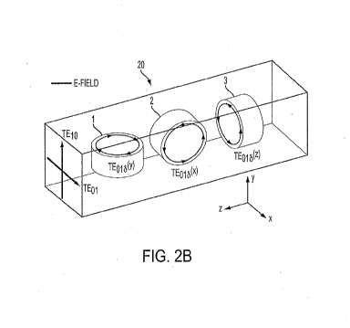
FIG. 2A is a perspective view of an evanescent waveguide with two orthogonally
oriented dielectric resonators, in accordance with an embodiment of the
present
invention.
FIG, 2B is a perspective view of an evanescent waveguide with three
orthogonally oriented dielectric resonators, in accordance with an embodiment
of the
present invention.
FIG. 3A is a perspective view of a triple resonator configuration in an
evanescent
io waveguide with two parallel metallic rods oriented at 45 degrees with
respect to a
horizontal plane of the waveguide, thereby providing negative coupling between
the
first and third resonator, in accordance with an embodiment of the present
invention.
FIG. 3B is a perspective view of the same triple resonator shown in FIG. 3A,
except that the two metallic rods are inverted, as they are oriented at +45
degrees and
at -45 degrees with respect to the horizontal plane of the waveguide, thereby
providing ,
positive coupling between the first and third resonator, in accordance with an
embodiment of the present invention.
FIG. 3C is a schematic diagram showing the electromagnetic coupling among
the various elements in the triple resonator configuration of FIG. 3A, in
accordance with
an embodiment of the present invention.
FIG. 4A is a plot of S parameters versus frequency for the triple resonator
configuration shown in FIG. 3A, in accordance with an embodiment of the
present
invention.
FIG. 4B is a plot of S parameters versus frequency for the triple resonator
configuration shown in FIG. 3B, in accordance with an embodiment of the
present
invention.
FIG. 5A is a perspective view of two-triple resonator configurations that are
cascaded in-line, thereby providing a 6th order filter, in accordance with an
embodiment
of the present invention.
FIG. 5B is a schematic diagram showing cascading of the various elements in
the 6th order filter shown in FIG. 5A, in accordance with an embodiment of the
present
invention.
FIG. 6 is a plot of S parameters versus frequency for the two-triple resonator
configurations shown in FIG. 5, including experimental results and simulated
results, in
accordance with an embodiment of the present invention.
FIGS. 7, 8 and 9 describe one form of electromagnetic coupling control for the
triple resonator configurations of FIGS. 3A and 3B, in which the overall
distance
CA 02874847 2014-11-26
WO 2013/188116 PCT/US2013/043253
- 3 -
between resonators, d, is varied, in accordance with an embodiment of the
present
invention.
FIGS. 10 and 11 describe another form of electromagnetic coupling control for
the triple resonator configurations of FIGS. 3A and 3B, in which the
penetration
distance, p, of a rod is varied, in accordance with an embodiment of the
present
invention.
FIG. 12A is a perspective view of a quadruple resonator configuration in an
evanescent waveguide with two waveguide steps realized at a corner of the
waveguide
(at the same side-wall), thereby providing positive coupling between the first
and
io fourth resonator, in accordance with an embodiment of the present
invention.
FIG. 12B is a perspective view of the same triple resonator shown in FIG. 12A,
except that the two waveguide steps are inverted, as they are realized at
different
corners of the two opposite side-walls, thereby providing negative coupling
between
the first and fourth resonator, in accordance with an embodiment of the
present
IS invention.
FIG. 12C is a schematic diagram showing the electromagnetic coupling among
the various elements in the quadruple resonator configuration of FIGS. 12A and
12B, in
accordance with an embodiment of the present invention.
FIG. 13A is a perspective view of a quadruple resonator configuration in an
20 evanescent waveguide with two waveguide steps realized at the top
surface of the
waveguide, thereby providing positive coupling between the first and fourth
resonator,
in accordance with an embodiment of the present invention.
FIG. 13B is a perspective view of the same quadruple resonator shown in FIG,
13A, except that the two waveguide steps are inverted, as they are realized
25 respectively at the bottom and top of the waveguide, thereby providing
negative
coupling between the first and fourth resonator, in accordance with an
embodiment of
the present invention.
FIG. 13C is a schematic diagram showing the electromagnetic coupling among
the various elements in the quadruple resonator configurations of FIGS. 13A
and 135,
30 in accordance with an embodiment of the present invention.
FIG. 14A is a plot of S parameters versus frequency for the quadruple
resonator
configurations shown in FIGS, 12A and 13A, in accordance with an embodiment of
the
present invention.
FIG. 14B is a plot of S parameters versus frequency for the quadruple
resonator
35 configurations shown in FIGS. 12B and 13B, in accordance with an
embodiment of the
present invention.
CA 02874847 2014-11-26
WO 2013/188116 PCT/US2013/043253
- 4 -
FIG. 15 is a perspective view of two-quadruple resonator configurations that
are
cascaded in-line, thereby providing an 8th order filter, in accordance with an
embodiment of the present invention.
FIG. 16 is a plot of S parameters versus frequency for the two-quadruple
resonator configurations shown in FIG. 15, including experimental results and
simulated results, in accordance with an embodiment of the present invention.
FIG. 17A is a perspective view of a quintuple resonator configuration in an
evanescent waveguide with two waveguide steps realized at opposite sidewalls
of the
waveguide, thereby providing negative coupling between the second and fourth
resonators, and a positive coupling between the first and fifth resonators, in
accordance
with an embodiment of the present invention.
FIG. 17B is a perspective view of the same quintuple resonator configuration -
shown in FIG. 17A, except that the two waveguide steps are realized at the
same
sidewall of the waveguide, thereby providing positive coupling between the
second and
fourth resonator, and negative coupling between the first and fifth resonator,
in
accordance with an embodiment of the present invention.
FIG. 17C is a schematic diagram showing the electromagnetic coupling among
the various elements in the quintuple resonator configurations of FIGS. 17A
and 17B, in
accordance with an embodiment of the present invention.
FIG. 18A is a plot of S parameters versus frequency for the quintuple
resonator
configuration shown in FIG. 17A, including experimental results and simulated
results,
in accordance with an embodiment of the present invention.
FIG. 18B is a plot of S parameters versus frequency for the quintuple
resonator
configuration shown in FIG. 17B, including experimental results and simulated
results,
in accordance with an embodiment of the present invention.
SUMMARY OF THE INVENTION
To meet this and other needs, and in view of its purposes, the present
invention provides a filter comprising an evanescent mode waveguide formed
along a
straight line and configured to receive at least two waveguide modes. A first
dielectric
resonator is disposed in the waveguide, and configured to be excited by one of
the two
waveguide modes, where the first dielectric resonator has an excited field
oriented in a
first plane that intersects with the straight line. A second dielectric
resonator is
disposed in the waveguide, and configured to be excited by the other one of
the two
waveguide modes, where the second dielectric resonator has an excited field
oriented
in a second plane that intersects with the straight line. The first and second
planes
intersect the straight line at different angles. A third dielectric resonator
is disposed in
the waveguide and configured to be substantially excited by the same waveguide
mode
CA 02874847 2014-11-26
WO 2013/188116 PCT11TS2013/0-13253
- 5 -
as the first dielectric resonator, where the third dielectric resonator has an
excited field
oriented in a third plane that intersects with the straight line The first and
third planes
are substantially parallel to each other.
The second dielectric resonator is disposed between the first and third
dielectric resonators. The second dielectric resonator is electromagnetically
coupled to
the first and third dielectric resonators. In addition, the first and third
dielectric
resonators are electromagnetically coupled to each other.
The filter may include a first perturbation element extending from an
external surface of the waveguide into the waveguide, where the first
perturbation
io element is disposed between the first and second dielectric resonators.
A second
perturbation element may extend from the external surface of the waveguide
into the
waveguide, where the second perturbation element is disposed between the
second
and third dielectric resonators. The first and second perturbation elements
may be
configured to excite the second dielectric resonator in a mode that is the
other of the
is mode that excites the first and third dielectric resonators.
The first perturbation element may be a first metallic rod oriented at a
positive or negative angle with respect to the first dielectric resonator. The
second
perturbation element may be a second metallic rod oriented at a positive or
negative
angle with respect to the third dielectric resonator. The first and second
metallic rods
20 may be substantially oriented at a positive or a negative 45 degree
angle with respect
to the first and third dielectric resonators, respectively. A penetration
distance, p, of
the first and second metallic rods into the waveguide is effective in
controlling an
amount of electromagnetic coupling between the first and second dielectric
resonators,
and between the second and third dielectric resonators, respectively. The
longer is the
25 penetration distance p, the greater is the amount of electromagnetic
coupling.
A distance, d, between a center of the first dielectric resonator and a
center of the third dielectric resonator is effective in controlling an amount
of
electromagnetic coupling between the first and third dielectric resonators.
The shorter
is the distance d, the greater is the amount of electromagnetic coupling.
30 Another embodiment of the present invention is a dielectric resonator
filter
comprising: first, second, third and fourth dielectric resonators cascaded
along a
straight line, and disposed in an evanescent mode waveguide. The first and
fourth
dielectric resonators are substantially parallel to each other, the second and
third
dielectric resonators are substantially parallel to each other. The first and
second
35 dielectric resonators are oriented at different angles along the
straight line. At least a
pair of non-adjacent dielectric resonators are electromagnetically coupled to
each
other.
CA 02874847 2014-11-26
WO 2013/188116 PCT/US2013/043253
- 6 -
A first perturbation element may extend from an external surface of the
waveguide into the waveguide, where the first perturbation element is disposed
between the first and second resonators. A second perturbation element may
extend
from the external surface of the waveguide into the waveguide, where the
second
perturbation element is disposed between the third and fourth resonators. The
first
and fourth dielectric resonators are electromagnetically coupled to each
other, and the
second and third dielectric resonators are electromagnetically coupled to the
first and
fourth dielectric resonators, respectively.
Yet another embodiment of the present invention is a dielectric resonator
filter
io comprising: (a) first, second, third, fourth and fifth dielectric
resonators cascaded along
a straight line, and (b) the dielectric resonators disposed in an evanescent
mode
waveguide. The first and fifth resonators are substantially parallel to each
other. The
second and fourth resonators are substantially parallel to each other. The
first and
second resonators are oriented at different angles along the straight line.
The third
is resonator is oriented at an angle that is different from either the
first and second
resonators. A first perturbation element may extend from an external surface
of the
waveguide into the waveguide, where the first perturbation element is disposed
between the first and second resonators. A second perturbation element may
extend
from the external surface of the waveguide into the waveguide, where the
second
zo perturbation element is disposed between the second and third
resonators. A third
perturbation element may extend from the external surface of the waveguide
into the
waveguide, where the third perturbation element is disposed between the third
and
fourth resonators. A fourth perturbation element may extend from the external
surface
of the waveguide into the waveguide, where the fourth perturbation element is
25 disposed between the fourth and fifth resonators. At least a pair of non-
adjacent
dielectric resonators may be electromagnetically coupled to each other.
It is understood that the foregoing general description and the following
detailed description are exemplary, but are not restrictive, of the invention.
DETAILED DESCRIPTION OF THE INVENTION
30 The present invention includes using single-mode TE01.6 dielectric
resonators (or TE01(1,o) mode, with arbitrary n) with different orientations
that are
cascaded along an evanescent mode waveguide. By using a pair of orthogonal
waveguide evanescent modes, namely TEN and TEN., which can excite or by-pass
the
resonators, cross-coupling between non-adjacent pucks is established and
properly
35 controlled. Compared to HEns and TEols mode filters, the present
invention maintains
a convenient in-line structure of the former, while having the flexibility and
spurious
performance of the latter.
CA 02874847 2014-11-26
WO 2013/188116 PCT/US2013/043253
- 7 -
The present invention may be understood by considering the structures
illustrated in FIGS. 2A and 2B. FIG. 2A shows two dielectric resonators having
different
orientations cascaded along an evanescent mode square waveguide 10. FIG. 2B=
shows
three dielectric resonators with different orientations, also cascaded along
an
evanescent mode square waveguide 20.
Referring first to FIG. 2A, the E-field of the TEDio mode in the first
dielectric resonator (labelled 1) lies on the xz plane. Such a field is
parallel to that of
the TE01 mode of the waveguide, while being orthogonal with respect to the
field of the
TEio mode. As a result, the TE01 mode can excite the resonator, while the TEio
mode
io cannot. The latter can only by-pass the resonant mode of the first
dielectric resonator,
which is seen as a simple dielectric obstacle. Analogous considerations are
applied to
the second dielectric resonator (labelled 2), where the resonant TE015 mode is
excited
by the TEio mode and is by-passed by the TE01 mode.
In this condition, the two dielectric resonators are, therefore, isolated
Is from each other. By introducing proper waveguide discontinuities, such
as field
perturbations, coupling mechanisms may be established. Direct-coupling and
cross-
coupling may be properly realized due to the by-pass coupling of the two
waveguide
evanescent modes.
Referring next to FIG. 2B, there is shown three dielectric resonators with
20 three different orthogonal orientations cascaded along an evanescent
mode waveguide
with square cross-section. The resonant modes of the dielectric resonators, as
well as
the evanescent modes of the waveguide, are indicated in the figure by their E-
fields.
In the following explanation, the coupling relationships between resonant and
waveguide modes are described by considering the orientation and the symmetry
of
25 the E-fields of the various modes. This is an arbitrary choice, as the
same conclusions
can be derived by considering the H-fields as well.
The E-field of the mode resonating in the first resonator (labelled 1 in
FIG. 2B), referred to as TE01' ) to indicate the y-axis orientation, lies on
the xz plane.
Such a field is parallel to that of the TE01 mode of the waveguide, while
being
30 orthogonal with respect to the field of the TE0 mode. As a result, the
TED' mode can
excite the resonator, while the TEio mode cannot. The latter can only by-pass
the
resonant mode of the first dielectric resonator, which is seen as a simple
dielectric
obstacle. Opposite considerations may be applied to the second dielectric
resonator
(labelled 2 in FIG. 2B), which is oriented along the x-axis. The resonant mode
TE016(x)
35 of the second resonator can be excited by the TEio mode, and by-passed
by the TE01
mode.
CA 02874847 2014-11-26
WO 2013/188116 PCT/US2013/043253
- 8 -
In contrast with the previous cases, neither TE10 nor TE01 modes can
excite the resonant mode TE016(z) of the third dielectric resonator (labelled
3 in FIG.
2B), which is located at the center of the waveguide cross-section. Although
the E-
fields of the resonant mode TE010(z) and of the evanescent modes TE10 and TE01
all lie
on the xy plane, due to symmetry reasons no coupling occurs among these modes.
Specifically, the resonant mode TE015(z) has odd symmetry with respect to both
x and y
axis, while the modes TED,. and TE10 have even symmetry with respect to the x
and y
axis, respectively. These two evanescent modes will by-pass the third
dielectric
resonator, while other TE modes with odd symmetry, such as TEN and TE02, can
excite
io the resonator.
It will be appreciated that the three dielectric resonators are isolated
from each other, because they are substantially orthogonal to each other and,
consequently, none of the evanescent modes can excite more than one resonator
at
the same time. Under these conditions, the three dielectric resonators are
isolated
from each other. By introducing proper waveguide discontinuities, such as
field
perturbations, or by changing the position of the dielectric resonators
(proper rotation
and/or offset) coupling mechanisms may be established. It will be further
appreciated
that coupling mechanisms may be established by orienting the dielectric
resonators to
lie in planes that are not orthogonal to each other. Either (or both) direct-
coupling and
.. cross-coupling may be properly realized by proper orientations of the
dielectric
resonators.
Moreover, although only the TE10, TE01, TE20, and TE02 modes have been
considered (lower order modes providing most of the contribution), the above
considerations hold true for all of the higher order modes of the waveguide.
Among the various embodiments that may be implemented by the
present invention, two structures are shown in FIGS. 3A and 3B, as examples of
basic
building blocks for pseudoelliptic filter design. Each waveguide structure 30,
35
includes three dielectric resonators, designated in sequence as R1, R2 and R3,
in which
the inner resonator R2 has an orthogonal orientation with respect to the outer
resonators R1 and R3. The outer resonators R1 and 1-t3 are oriented along the
same
axis. In the examples of FIGS. 3A and 3B, the outer resonators are oriented
along the
y-axis and the inner resonator R2 is oriented along the x-axis. Metallic rods
31 and 32
are oriented at the same 45 degree angle (also referred to as parallel rods)
in FIG. 3A,
while metallic rods 36 and 37 are oriented at opposite 45 degree angles with
respect to
a center line extended along a width dimension of structure 35 (also referred
to as
inverted rods) in FIG. 3B. Input and output probes 38 and 39, respectively,
are also
CA 02874847 2014-11-26
WO 2013/188116 PCT/US2013/043253
- 9 -
shown in FIGS. 3A and 3B. It will be understood that other orientations, such
as z-axis
for the inner or the outer resonators, are also possible and lead to the same
results.
The mode operation within waveguide structures 30, 35 is illustrated by
the block diagram in FIG. 3C. The input and output probes excite the resonant
mode in
the first (R1) and last (R3) resonators, respectively. The first and last
resonators are
coupled by the evanescent TE01 mode, which by-passes the second resonator
(R2).
Metallic rods with 45 degree orientation are used to generate a coupling
between the
TE01 and the TE10 modes of the waveguide. In this way, part of the energy is
transferred to the second resonator R2, which is excited by the TEio mode, as
shown in
FIG. 3C.
The resulting topology, shown in FIGS. 3A, 3B and 3C, may be referred
to as a triplet configuration, which generates 3rd order filtering functions
with a
transmission zero that can be located either below, or above the passband,
depending
on the sign (positive or negative) of the by-pass coupling, as explained
below.
Both positive and negative signs can be obtained by inverting the phase
of the excited field at the outer resonators in the direct-path with respect
to the phase
of the by-passing mode. In practice, this may be accomplished by moving the
second
45 degree rod from the bottom to the top wall of the waveguide, as shown in
FIG. 3B
by rod 37. The latter configuration is referred to herein as inverted rods, as
compared
to the configuration of parallel rods shown in FIG. 3A.
FIGS. 4A and 4B depict HFSS simulations (lossless) of the two filter
configurations (shown in FIGS. 3A and 3B, respectively) having a transmission
zero in
the lower and upper stopband, respectively. It will be appreciated that these
figures
represent transfer characteristics (or S-parameters) that show the frequency
response
of the two filters constructed in accordance with the present invention.
Transfer
characteristics, such as those shown in FIGS. 4A and 4B, are typically
generated using
equipment such as a network analyzer. The output signal from the network
analyzer is
generally coupled into an input port. As the network analyzer generates the
output
signal, it measures a signal at another port (e.g., the output port). The
network
analyzer then computes a ratio of the output signal at each frequency. Two
typical
measurements performed by the network analyzer are S21 (insertion loss), which
is a
ratio of a signal output from port 2 (e.g., the output port) to a signal input
to port 1
(e.g., the input port); and S11 (return loss), which is a ratio of a signal
output form port
1 (e.g., the input port) to a signal input to port 1 (e.g., the input port).
Accordingly, FIG. 4A shows the simulated S-parameters of the
configuration shown in FIG. 3A (the triple-resonator configuration with
parallel rods).
CA 02874847 2014-11-26
WO 2013/188116
PCT/US2013/043253
- 10 -
FIG. 45 shows the simulated S-parameters of the configuration shown in FIG. 36
(the
triple-resonator configuration with inverted rods).
The size of each 45 degree rod, in FIGS. 3A and 3B, adjusts the direct-
coupling between one resonator and its adjacent resonator, namely, the more
penetration, the stronger the coupling. The distance between the resonators
impacts
the by-pass coupling without significantly affecting the direct-coupling. As a
result, the
position of the transmission zero may be adjusted, while maintaining a
consistent
passband.
In another embodiment of the present invention, FIGS. 5A and 56 show
lo a 6th order filter that uses two triplet configurations, designated as
structures 50 and
52. The filter structure cascades triplet structure 50 and triplet structure
52, as shown
in FIG 56.
An HFSS simulation (lossless) and an experimental result for the two
triplet configurations of FIG. 5A are depicted in FIG.6. The filter structure
includes low-
permittivity dielectric supports and tuning elements. The filter has 0.55%
fractional
bandwidth at 2.170 GHz and provides high selectivity at the lower stopband,
due to a
pair of transmission zeros. High permittivity dielectric pucks with 5000 Q-
factor are
included. The measured insertion loss is 1.35 dB at the filter center
frequency.
The coupling coefficients of the waveguide structure can be controlled by
adjusting the distances between the resonators, as well as the dimensions of
the
oblique rods.
With reference to FIGS. 7, 8 and 9, once the waveguide cross-sectional
dimensions are set, the distance d between the outer resonators is the main
parameter
to control the by-pass coupling 1(13. Observe that the by-pass coupling
primarily occurs
through the TEoi mode of the waveguide.
FIG. 9 shows the magnitude of the by-pass coupling coefficient k13
versus the distance d for a fixed cross-sectional size. As d increases, the
coupling k13
decreases due to the decay of the evanescent TED,. mode. Observe that no
sequential
coupling k12 and 1<23 are present in the structure of FIG. 7.
The sequential coupling coefficients Ku and k23 depicted in FIG. 10 are
generated by inserting oblique metallic rods among the resonators. FIG. 3A
shows a
pair of oblique metallic rods (45 ) inserted between resonators. The
penetration p of
the rod controls the coupling coefficient. FIG. 11 shows the magnitude of the
coupling
k12 versus the penetration p for a fixed cross-sectional size. The more the
penetration
the stronger the coupling, as a stronger interaction between the TE01 and TEio
modes is
generated through the oblique rod.
CA 02874847 2014-11-26
WO 2013/188116 PCT/US2013/043253
- 11 -
As previously described, the transmission zero can be moved to the other
side of the passband by simply inverting the position of one of oblique rods
as is shown
in the structure of FIG. 35. In this condition, the magnitude of the coupling
coefficients
remains basically unchanged, while the by-pass coupling sign is inverted.
Other embodiments that may be implemented by the present invention
are shown in FIGS. 12A, 12B, 13A and 13B. These embodiments are additional
basic
building blocks for pseudoelliptic filters that are referred to herein as
quadruple-
resonator configurations. Each waveguide structure includes a cascade of four
dielectric resonators, where the inner resonator pair is orthogonally oriented
with
lo respect to the outer resonator pair. The input port is designated as 125
and the output
port is designated as 126.
It will be noted that ring-shaped resonators 121, 122, 123 and 124
(disk-shaped with a hole in the center) are used in the waveguide structures
designated as 120 and 130 in FIGS. 12A and 125, respectively. On the other
hand,
is disk-shaped resonators 141, 142, 144 and 145 are used in the waveguide
structures
designated as 140 and 150 in FIGS. 13A and 135, respectively. The resonators
may
also employ modes supported by other shapes with resonant eigen-mode
solutions,
such as rectangular parallopipeds, spheres, elliptical shapes, etc.
It will be appreciated that the waveguide structures need not be of
20 rectangular cross-section, and may employ modes common to round or
elliptical
waveguides, with appropriate evanescent modes selected for coupling or
bypassing the
dielectric resonators contained within the respective waveguide structure.
The mode operation occurring within the waveguide structures of FIGS.
12A and 12B is illustrated by the block diagram in FIG. 12C. The first and
last
25 resonators are coupled by the evanescent TE01 mode, which by-passes the
second and
third resonators. Stepped corners 127 and 128 formed on the same side-wall of
waveguide structure 120 in FIG. 12A and stepped corners 131 and 132 formed on
opposite side-walls of waveguide structure 130 in FIG. 125 are used in these
embodiments to generate a coupling between the TEci and the TEio modes of the
30 waveguide, as best shown in FIG. 12C. In this manner, a portion of the
energy is
transferred from the outer resonator pair to the inner resonator pair.
It will be noted that the stepped corners are similar to the oblique rods
used in the triplet configurations of FIGS. 3A and 35. The oblique rods may
also be
used instead of the stepped corners in FIGS. 12A and 12B. Thus, rods or
stepped
35 corners, or any other type of waveguide discontinuity may be used by the
present
invention to generate coupling mechanisms between orthogonal modes. It will
also be
appreciated that an additional waveguide discontinuity, such as an iris, may
be used
CA 02874847 2014-11-26
WO 2013/188116 PCT/US2013/043253
- 12 -
between the second and third resonators (which have the same orientation) to
modulate the coupling occurring between them.
The mode operation occurring within the waveguide structures of FIGS.
13A and 13B are illustrated by the block diagram in FIG. 13C. The first and
last
resonators are coupled by the evanescent TEoi mode, which by-passes the second
and
third resonators. Asymmetric steps realized within the waveguide structure are
used to
generate a coupling between the TE01 and the TE02 modes of the waveguide. As
shown, asymmetric steps 146 and 147 are formed on the same top surface of
waveguide structure 140, while asymmetric steps 151 and 152 are formed on
opposite
io top and bottom surfaces of waveguide structure 150. In this manner, a
portion of the
energy is transferred from the outer resonator pair to the inner resonator
pair (rods
may be also used for the same purpose).
The resulting topology shown in FIGS. 12A, 125, 12C, 13A, 135 and 13C
(also referred to as a quadruplet configuration) generates 4rd order filtering
functions
is with two zeros that may be located either on the imaginary axis of a
complex plane
(finite frequency transmission zeros), or on the real axis of the complex
plane (group
delay equalization), 'depending on the sign (negative or positive) of the by-
pass
coupling, as explained below.
Both positive and negative signs may be obtained by inverting the phase
20 of the excited field at the outer resonators in the direct-path with
respect to the phase
of the by-passing mode. In practice, this may be accomplished by moving one of
the
stepped corners to the opposite waveguide side-wall, as shown in FIG.12B, or
by
moving one of the asymmetric steps from the top to the bottom of the
waveguide, as
shown in FIG. 135. The latter two configurations are also referred to herein
as inverted
25 steps, as compared to the parallel steps shown in FIG. 12A and FIG. 13A.
FIGS. 14A and 145 depict HFSS simulations (lossless) of the quadruple-
resonator configurations. FIG. 14A shows the simulated S-parameters of the
configurations depicted in FIGS. 12A and 13A (the quadruple-resonator
configurations
with parallel steps). FIG. 14B shows the simulated S-parameters of the
configurations
30 depicted in FIGS. 12B and 13B (the quadruple-resonator configurations
with inverted
steps).
The size of each step in FIGS. 12A, 125, 13A and 13B adjusts the direct-
coupling between two adjacent orthogonal resonators, namely, the larger the
size of
the step, the stronger the coupling. The distance between the resonators
impacts the
35 by-pass coupling without significantly affecting the direct-coupling. As
a result, the
position of the transmission zero may be adjusted while maintaining a
consistent
passband.
CA 02874847 2014-11-26
WO 2013/188116 PCT/US2013/043253
- 13 -
In yet another embodiment of the present invention, FIG. 15 shows an
81h order filter that uses two quadruplet configurations, designated as 150
and 151.
The filter structure includes tuning elements, generally designated as 152
that may be
inserted within each center hole of a respective disk shaped resonator (not
labeled).
An HFSS simulation (lossless) and an experimental result are shown in
FIG. 16 for the 8th order filter of FIG. 15. As an example, the filter has
0.457%
fractional bandwidth at 4.810 GHz and provides high selectivity at both sides
of the
passband, due to two pairs of transmission zeros. High permittivity dielectric
pucks
with 15000 Q-factor may be included. As an example, the measured insertion
loss is
I() 1.40 dB at the filter center frequency (7000 cavity Q-factor).
Still more embodiments of the present invention are shown in FIGS. 17A
and 17B. These embodiments are additional basic building blocks for
pseudoelliptic
filters that are referred to herein as quintuple-resonator configurations
designated,
respectively, as 170 and 180. Each structure includes a cascade of five
dielectric
is resonators, namely 171, 172, 173, 174 and 175, where the inner most
resonator 173 is
orthogonally oriented with respect to the other resonators, and where the
second and
fourth resonators 172, 174 are orthogonally oriented with respect to the first
and fifth
resonators 171, 175.
The mode operation occurring within the waveguide structures of FIGS.
20 17A and 17B is illustrated by a block diagram in FIG. 17C. As shown, the
first and last
resonators are coupled by the evanescent TEoi mode, which by-passes the
second,
third and fourth resonators. The second and fourth resonators are coupled one
to the
other by the evanescent TEio mode which by-passes the third resonator. First
and
second resonators (as well as fourth and fifth resonators) are coupled to each
other by
25 oblique metallic rods 176, which generate an interaction between the
TE01 and the TEio
modes. The third resonator is coupled to the second and fourth resonators by
asymmetric steps 181, which generate an interaction between the TE10 and the
TE20
modes.
The resulting topology depicted in FIGS. 17A, 17B and 17C, which may
30 be referred to as a quintuplet configuration, generates 5th order
filtering functions with
three finite frequency transmission zeros.
The relative position of the asymmetric steps with respect to each other,
determines the signs of the by-pass coupling coefficients. The structure 170
in FIG.
17A, in which steps 181 are realized on opposite waveguide sidewalls (inverted
steps),
35 yields a negative sign for the by-pass coupling between the second and
fourth
resonator, while giving a positive sign for the by-pass coupling between the
first and
the fifth resonator. On the other hand, structure 180 in FIG. 17B, in which
the two
CA 02874847 2014-11-26
WO 2013/188116 PCT/US2013/043253
- 14 -
asymmetric steps, are realized on the same waveguide sidewall (parallel
steps), yields a
positive sign for the by-pass coupling between the second and fourth resonator
while
giving a negative sign for the by-pass coupling between the first and the
fifth
resonator.
As previously described for the triple and quadruple configurations, the
size of each step 181 and each oblique rod 176 in FIGS. 17A and 17B adjusts
the
direct-coupling between two adjacent orthogonal resonators, while the
distances
between the resonators impacts the by-pass coupling coefficients.
FIGS. 18A depicts the HFSS simulation (lossless) and measurements of
lo the quintuple-resonator configuration in FIG. 17A (configuration with
inverted steps).
FIGS. 18B depicts the HFSS simulation (lossless) and measurements of the
quintuple-
resonator structure configuration of FIG. 17B (configuration with parallel
steps).
It will be understood that the waveguides may be circular, rather than
square. In the embodiments described, the waveguides were shown as square or
is rectangular. In addition, although in the embodiments two modes were
generally
described, nevertheless, there may be an infinite number of modes that
contribute to
the excitation of the resonators. It is more accurate to state that the
resonator may be
excited substantially by a particular mode, but may include additional modes.
Furthermore, the resonators do not need to be 100% orthogonal to each
20 other. In general, the resonators may be differently oriented from each
other. When
the resonators are 100% orthogonal along one of the three axes, the properties
of the
structure are optimized from certain perspectives, but the present invention
still works
when the resonators are only partially orthogonal to each other.
Moreover, the resonators are electromagnetically uncoupled from each
25 other only if the resonators are 100% orthogonal and if no perturbations
are introduced
in the waveguide. This condition typically would not occur, as there needs to
be an
electromagnetic coupling between the resonators. The perturbations allow the
generation of an interaction between the waveguide modes which excite each of
the
resonators. Thus, the resonators are coupled to each other and the purpose of
the
30 .. perturbations is to control the amount of coupling between them.
Although the invention is illustrated and described herein with reference
to specific embodiments, the invention is not intended to be limited to the
details
shown. Rather, various modifications may be made in the details within the
scope and
range of equivalents of the claims and without departing from the invention.