Note: Descriptions are shown in the official language in which they were submitted.
CA 02874992 2014-12-16
1
TITLE OF THE INVENTION
SEMICONDUCTOR LASER LIGHT SOURCE
BACKGROUND OF THE INVENTION
Field of the Invention
The present invention relates to high-output semiconductor laser light sources
including a high-output semiconductor laser and a sub-mount which are bonded
to each
other and, more particularly, relates to structures capable of efficiently
dissipating heat
generated from a semiconductor laser through a sub-mount for improving output
characteristics and reliability of a semiconductor laser light source.
Description of the Background Art
Semiconductor lasers output laser light and also generate heat during
operations.
In general, semiconductor lasers exhibit improved output characteristics and
improved
reliability at lower temperatures and, therefore, it is important to dissipate
heat therefrom.
As heat sinks for heat dissipation, there have been utilized members made of
high-heat-radiation metal materials (for example, Cu). However, such heat
sinks made
of Cu and the like have linear expansion coefficients larger titan
semiconductor lasers,
which makes it harder to directly bond them to each other. Therefore, in
general, a
semiconductor laser is bonded to a sub-mount made of a material having a
linear
expansion coefficient with a value between those of a heat sink and the
semiconductor
laser, and the sub-mount is bonded to the heat sink.
In such cases, for bonding a semiconductor laser to a sub-mount, there have
been structures which place an Au layer on the bonding surface of the
semiconductor
laser and, further, place an Au/Pt/AuSn solder layer on the sub-mount, for
bonding them
CA 02874992 2014-12-16
2
to each other.
For example, Japanese Patent Application Laid-Open No. 5-190973 (1993)
discloses a structure having a semiconductor laser and a sub-mount which are
bonded to
each other, wherein the sub-mount includes a sub-mount substrate, a Ti layer,
a Pt layer
and an Au layer which are placed on the sub-mount substrate, and a Pt layer
and an AuSn
solder layer which have the same length as that of the semiconductor laser and
are placed
on the upper surface of the Au layer.
For example, Japanese Patent Application Laid-Open No. 2002-359425
discloses a structure having a semiconductor laser and a sub-mount which are
bonded to
each other, wherein the sub-mount includes a sub-mount substrate, a Ti/Pt
layer and an
Au layer which are placed on the sub-mount substrate, a barrier layer which
has a length
smaller than that of the semiconductor laser and is placed on the upper
surface of the Au
layer, and a solder layer formed to cover the barrier layer.
SUMMARY OF THE INVENTION
In the structure described in Japanese Patent Application Laid-Open No.
5-190973 (1993), the Pt layer and the AuSn solder layer, which have the same
length as
that of the semiconductor laser, are placed on the sub-mount substrate, which
causes the
AuSn solder to spread with wetness toward the Au layer placed over the entire
surface of
the sub-mount substrate, during the bonding. In this case, there may be
induced
variations in the members, such as variations in the surface roughness of the
sub-mount
substrate, and the thickness and the composition ratio of the AuSn solder
layer and, also,
there may be induced variations in the bonding conditions such as the
temperature and the
load applied thereto during the bonding.
When there are induced such variations in the members or such variations in
the
bonding conditions, the amount of the solder on the lower surface of the
semiconductor
CA 02874992 2014-12-16
3
laser is not stabilized, which causes voids on the lower surface of the
semiconductor laser.
This has induced the problem of degradation of the output characteristics and
the
reliability of the semiconductor laser light source.
Further, in the structure described in Japanese Patent Application Laid-Open
No.
2002-359425, there is placed, on the sub-mount substrate, the solder layer
formed to
cover the barrier layer (a Pt layer, for example) having a length smaller than
that of the
semiconductor laser, which causes the AuSn solder to spread with wetness
toward the Au
layer placed over the entire surface of the sub-mount substrate, during the
bonding. This
has induced the same problem as that of Japanese Patent Application Laid-Open
No.
5-190973 (1993).
It is an object of the present invention to provide a semiconductor laser
light
source capable of exhibiting improved output characteristics and improved
reliability,
even when there are variations in members and variations in bonding
conditions.
A semiconductor laser light source according to the present invention includes
a
semiconductor laser having an output end for outputting laser light, and a sub-
mount to
which the semiconductor laser is bonded. The sub-mount includes a sub-mount
substrate, an Au layer placed above the sub-mount substrate, a barrier layer
which is
placed on the Au layer and has a wall portion at least in a portion of its
outer peripheral
portion which is other than a portion corresponding to a side of the output
end of the
semiconductor laser, and a solder layer placed on the barrier layer in an area
surrounded
by the wall portion. The semiconductor laser is bonded to the sub-mount
through the
solder layer, in a state where the semiconductor laser is spaced apart by a
predetermined
interval from an inner surface of the wall portion, and further, the output
end protrudes, in
a direction of output of the laser light, from an end of the solder layer
which corresponds
to the side of the output end of the semiconductor laser.
CA 02874992 2014-12-16
4
The sub-mount includes the barrier layer which is placed on the Au layer and
has the wall portion at least in the portion of its outer peripheral portion
which is other
than the portion corresponding to a side of the output end of the
semiconductor laser, and
the solder layer placed on the barrier layer in the area surrounded by the
wall portion.
The semiconductor laser is bonded to the sub-mount through the solder layer,
in the state
where the semiconductor laser is spaced apart by the predetermined interval
from the
inner surface of the wall portion, and further, the output end protrudes, in
the direction of
output of the laser light, from the end of the solder layer which corresponds
to the side of
the output end of the semiconductor laser.
Accordingly, when the semiconductor laser is bonded to the sub-mount, a
portion of the redundant solder in the solder layer is gathered between the
outer peripheral
portion of the semiconductor laser and the wall portion in the barrier layer,
while a
remaining portion of the redundant solder is spread with wetness, toward the
portion
beneath the output end of the semiconductor laser, which protrudes in the
direction of
laser-light output. The redundant solder in the solder layer does not spread
with wetness
up to the side surfaces of the semiconductor laser which are other than the
output end,
which can stabilize the amount of the solder on the lower surface of the
semiconductor
laser, even in the event of occurrences of variations in the members or
variations in the
bonding conditions. This enables dissipating heat from the entire
semiconductor laser
with higher efficiency, thereby improving the output characteristics and the
reliability of
the semiconductor laser light source.
These and other objects, features, aspects and advantages of the present
invention will become more apparent from the following detailed description of
the
present invention when taken in conjunction with the accompanying drawings.
BRIEF DESCRIPTION OF THE DRAWINGS
CA 02874992 2014-12-16
FIG. 1 is a cross-sectional view illustrating a semiconductor laser light
source
according to a first preferred embodiment in a state where a semiconductor
laser has not
been bonded to a sub-mount;
FIG. 2 is a plan view of the semiconductor laser light source according to the
5 first preferred embodiment;
FIG. 3 is a cross-sectional view taken along the line A-A in FIG. 2;
FIG. 4 is a cross-sectional view taken along the line B-B in Fig. 2;
FIG. 5 is a view of an example of modification of the first preferred
embodiment, which corresponds to FIG. 3;
FIG. 6 is a cross-sectional view illustrating a semiconductor laser light
source
according to a second preferred embodiment in a state where a semiconductor
laser has
not been bonded to a sub-mount;
FIG. 7 is a cross-sectional view of the semiconductor laser light source
according to the second preferred embodiment;
FIG. 8 is a cross-sectional view illustrating a semiconductor laser light
source
according to a third preferred embodiment in a state where a semiconductor
laser has not
been bonded to a sub-mount;
FIG. 9 is a plan view of the semiconductor laser light source according to the
third preferred embodiment; and
FIG. 10 is a cross-sectional view taken along the line C-C in FIG. 9.
DESCRIPTION OF THE PREFERRED EMBODIMENTS
(First Preferred Embodiment)
Hereinafter, a first preferred embodiment of the present invention will be
described, with reference to the drawings. Fig. 1 is a cross-sectional view
illustrating a
semiconductor laser light source according to the first preferred embodiment
in a state
CA 02874992 2014-12-16
6
where a semiconductor laser 1 has not been bonded to a sub-mount 2. Fig. 2 is
a plan
view of the semiconductor laser light source according to the first preferred
embodiment.
Fig. 3 is a cross-sectional view taken along the line A-A in Fig. 2, and Fig.
4 is a
cross-sectional view taken along the line B-B in Fig. 2.
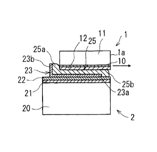
As illustrated in Fig. 1, the semiconductor laser light source includes the
semiconductor laser 1 and the sub-mount 2. The semiconductor laser 1 has a
multi-emitter structure having plural light emission points, for example.
The
semiconductor laser 1 includes a semiconductor laser substrate 11, an active
layer 10, and
an Au layer 12.
The active layer 10 is placed on the lower surface, in Fig. 1, of the
semiconductor laser substrate 11. By maintaining the active layer 10 at a
lower
temperature, it is possible to improve the output characteristics and the
reliability of the
semiconductor laser light source. Therefore, it is desirable that the
semiconductor laser
1 is bonded, in the side of the active layer 10, to the sub-mount 2. The Au
layer 12 is
placed, for bonding through soldering, on the lower surface of the active
layer 10 in the
semiconductor laser 1.
The sub-mount 2 includes a sub-mount substrate 20, an intermediate layer 21,
an Au layer 22, a barrier layer 23, and a solder layer 25. The sub-mount
substrate 20 is
desirably formed from a material having a linear expansion coefficient between
those of
the semiconductor laser 1 and a heat sink (not illustrated). In this case, the
heat sink is
formed from a high-heat-radiation metal material (for example, Cu).
'Therefore, the
sub-mount substrate 20 is formed from AIN or SiC which is a material having a
linear
expansion coefficient between those of the semiconductor laser 1 and the heat
sink.
The intermediate layer 21 can be either formed to be a Ti-layer/Pt-layer or
formed to have a multi-layer structure for the sake of further reduction of
the stress
CA 02874992 2014-12-16
7
exerted on the semiconductor laser 1 ill the event of linear expansion. For
example, the
sub-mount substrate 20 is formed from SiC, and the intermediate layer 21 is
formed to be
a Ti-layer/Cu-layer/Ni-layer such that the Ti layer exists next to the sub-
mount substrate
20. Thus, by adjusting the thicknesses of the respective layers in the
intermediate layer
21, it is possible to reduce the stress exerted on the semiconductor laser 1,
after the
bonding.
The Au layer 22 is placed on the upper surface of the intermediate layer 21.
The barrier layer 23 is placed on the upper surface of the Au layer 22, in the
area other
than the outer peripheral portion. The barrier layer 23 includes a horizontal
portion 23a
and a barrier portion 23b (a wall portion).
The horizontal portion 23a is formed to have a rectangular shape in a plan
view
and, further, is placed on the Au layer 22 in the area other than the outer
peripheral
portion thereof. The barrier portion 23b is provided on the outer peripheral
portion of
the horizontal portion 23a, at least in the portion thereof other than the
portion
corresponding to a side of an output end 1 a of the semiconductor laser 1. In
this case,
the output end la is the portion for outputting laser light, in the
semiconductor laser 1.
More specifically, the barrier portion 23b is formed, on the rectangular-
shaped
horizontal portion 23a, to have a wall shape protruding upwardly from the
outer
peripheral portion of the horizontal portion 23a which corresponds to its
three sides other
than the side coincident with the output end la of the semiconductor laser I.
In this case,
the barrier layer 23 (namely, the horizontal portion 23a and the barrier
portion 23b) can
be also formed from Pt. Further, the barrier portion 23b can be also formed by
performing vapor deposition of Pt inside a mask formed on the outer peripheral
portion of
the horizontal portion 23a and, thereafter, applying resist to the mask. The
solder layer
25 is placed on the barrier layer 23, in the area surrounded by the barrier
portion 23b.
CA 02874992 2014-12-16
8
The solder layer 25 is formed from AuSn.
As illustrated in Figs. 2 and 3, the semiconductor laser 1 is bonded to the
sub-mount 2 through the solder layer 25, in a state where the semiconductor
laser 1 is
spaced apart by a predetermined interval from the inner surface of the barrier
portion 23b,
and further, the output end la protrudes, in the direction of laser-light
output (in the
direction of an arrow in Fig. 3), from the end of the solder layer 25 which
coincides with
the output end la of the semiconductor laser 1.
The semiconductor laser 1, the barrier layer 23 and the solder layer 25 will
be
described, regarding their widths and lengths. As illustrated in Fig. 2, there
is the
following relationship between the width W1 of the semiconductor laser 1, the
width W2
of the solder layer 25, and the width W3 between the opposite ends of the
barrier portion
23b.
W1 < W2 < W3
Further, in the semiconductor laser 1, there is the following relationship
between the length LI to the rear end surface of the semiconductor laser 1
from the end of
the barrier portion 23b which is closer to the output end la, the length L2
therefrom to the
barrier portion including the barrier layer 23, and the length L3 of the
solder layer 25
before the bonding.
L1 < L2 < L3
The bonding of the semiconductor laser 1 to the sub-mount 2 is performed, by
raising the temperature of the sub-mount 2 to a temperature equal to or higher
than the
temperature which melts the solder layer 25 and, further, by applying a load
to the
semiconductor laser 1. Therefore, as illustrated in Figs. 3 and 4, after the
bonding, the
solder layer 25 has a thickness reduced from that of the solder layer 25
before the bonding,
which causes a partial solder 25a out of the redundant solder in the solder
layer 25 to
CA 02874992 2014-12-16
9
gather between the outer peripheral portion of the semiconductor laser 1 and
the barrier
portion 23b in the barrier layer 23. In this case, the barrier portion 23b
prevents the
redundant solder 25a from flowing to the outside of the barrier portion 23b.
For example, in cases where the bonding is performed at a higher temperature,
the solder tends to spread widely with wetness, but the barrier portion 23b
maintains the
amount of the solder on the lower surface of the semiconductor laser 1
constant. Further,
when the sub-mount substrate 20 and the intermediate layer 21 have higher
surface
roughness, the volume of the solder before the bonding may be different from a
targeted
volume, or the amount of the solder required for filling the concavity and
convexity in the
surfaces of the sub-mount substrate 20 and the intermediate layer 21 may be
varied.
Even in these cases, the amount of the solder on the lower surface of the
semiconductor
laser 1 is maintained constant, through the increase and decrease of the
redundant solder
25a.
Further, as described above, the semiconductor laser 1 is bonded to the
sub-mount 2 through the solder layer 25, in the state where the output end la
for
outputting laser in the semiconductor laser 1 protrudes, in the direction of
laser-light
output, from the end of the solder layer 25 which corresponds to the side of
the output end
la. By bonding them at this position, the active layer 10 is not obstructed
by the solder
layer 25. As an example of the length of the protrusion of the output end la
of the
semiconductor laser 1 from the end of the solder layer 25, the length of the
protrusion
may be about 20 micrometers. Since the barrier portion 23b does not exist in
the side
closer to the output end la of the semiconductor laser 1, a solder 25b which
is a
remaining portion of the redundant solder is spread with wetness, toward the
portion
beneath the output end la of the semiconductor laser 1 due to the bonding.
Thus, the
semiconductor laser 1 is bonded thereto through the solder over its
substantially-entire
CA 02874992 2014-12-16
lower surface, which can further improve the output characteristics and the
reliability of
the semiconductor laser light source.
As described above, in the semiconductor laser light source according to the
first preferred embodiment, the sub-mount 2 includes the barrier layer 23
which is placed
5 on the Au layer and has the barrier portion 23b at least in the portion
of its outer
peripheral portion which is other than the portion corresponding to a side of
the output
end la of the semiconductor laser 1, and the solder layer 25 placed on the
barrier layer 23
in the area surrounded by the barrier portion 23b, wherein the semiconductor
laser 1 is
bonded to the sub-mount 2 through the solder layer 25, in the state where the
10 semiconductor laser 1 is spaced apart by a predetermined interval from
the inner surface
of the barrier portion 23b, and further, the output end la protrudes, in the
direction of
laser-light output, from the end of the solder layer 25 which corresponds to
the side of the
output end la of the semiconductor laser I.
Accordingly, when the semiconductor laser 1 is bonded to the sub-mount 2, the
partial solder 25a, out of the redundant solder in the solder layer 25, is
gathered between
the outer peripheral portion of the semiconductor laser 1 and the barrier
portion 23b in the
barrier layer 23. The solder 25b which is a remaining portion of the redundant
solder is
spread with wetness, toward the portion beneath the output end 1 a of the
semiconductor
laser 1, which protrudes in the direction of laser-light output. The redundant
solder in
the solder layer 25 does not spread with wetness up to the side surfaces of
the
semiconductor laser 1 which are other than the output end I a, which can
stabilize the
amount of the solder on the lower surface of the semiconductor laser 1, even
in the event
of occurrences of variations in the members or variations in the bonding
conditions.
This enables dissipating heat from the entire semiconductor laser 1 with
higher efficiency,
thereby improving the output characteristics and the reliability of the
semiconductor laser
CA 02874992 2014-12-16
light source.
Due to the improvement of the output characteristics of the semiconductor
laser
light source, it is possible to reduce the amount of energy consumption in the
semiconductor laser light source. Further, due to the improvement of the
reliability of
the semiconductor laser light source, it is possible to use the semiconductor
laser light
source for a longer time period. Further, since the amount of the solder on
the lower
surface of the semiconductor laser 1 is stabilized, it is possible to increase
the yield of the
semiconductor laser light source.
Further, as described above, when the sub-mount substrate 20 is formed from
SiC, and there is provided the intermediate layer 21 which is placed between
the
sub-mount substrate 20 and the Au layer 22 and is formed from a
Ti-layer/Cu-layer/Ni-layer, it is possible to reduce stress strains during the
bonding,
which are caused by the linear expansion difference between the semiconductor
laser 1
and the sub-mount substrate 20. This can realize the seiniconductor laser
light source
with higher reliability which is capable of reducing the stress exerted on the
semiconductor laser 1 after the bonding.
Next, an example of modification of the first preferred embodiment will be
described. As illustrated in Fig. 5, another intermediate layer 21 can be also
placed on
the lower surface of the sub-mount substrate 20. Fig. 5 is a view of the
example of
modification of the first preferred embodiment, which corresponds to Fig. 3.
As
described above, another intermediate layer 21 is also placed on the lower
surface of the
sub-mount substrate 20, namely the upper and lower intermediate layers 21 are
placed
with the sub-mount substrate 20 sandwiched therebetween, which enables fine
adjustments of the linear expansion coefficient through the bimetal effect,
thereby further
reducing the stress exerted on the semiconductor laser 1 after the bonding.
Since the
CA 02874992 2014-12-16
12
stress exerted on the semiconductor laser I can be reduced, it is possible to
improve the
reliability of the semiconductor laser light source.
(Second Preferred Embodiment)
Next, a semiconductor laser light source according to a second preferred
embodiment will be described. Fig. 6 is a cross-sectional view illustrating
the
semiconductor laser light source according to the second preferred embodiment
in a state
where a semiconductor laser 1 has not been bonded to a sub-mount 32. Fig. 7 is
a
cross-sectional view of the semiconductor laser light source according to the
second
preferred embodiment. Further, in the second preferred embodiment, the same
components as those described in the first preferred embodiment are designated
by the
same reference characters and will not be described herein.
As illustrated in Figs. 6 and 7, in the second preferred embodiment, an Au
film
31 is placed on the side surface of the sub-mount 32 which coincides with an
output end
1 a of the semiconductor laser 1. Further, the other structures of the sub-
mount 32 are
the same as those in the structure of the sub-mount 2.
As described above, in the semiconductor laser light source according to the
second preferred embodiment, the Au film 31 is placed on the side surface of
the
sub-mount 32 which corresponds to the side of the output end I a of the
semiconductor
laser 1, which causes a redundant solder 25c after the bonding to spread with
wetness
along the Au film 31 on the side surface of the sub-mount 32. Even when there
is an
excessive amount of solder in a solder layer 25, it is possible to prevent an
active layer 10
corresponding to the side of the output end 1 a of the semiconductor laser 1
from being
obstructed in the redundant solder 25c. This reduces the rate of occurrences
of failures
in semiconductor laser light sources, thereby increasing the yield.
(Third Preferred Embodiment)
CA 02874992 2014-12-16
13
Next, a semiconductor laser light source according to a third preferred
embodiment will be described. Fig. 8 is a
cross-sectional view illustrating the
semiconductor laser light source according to the third preferred embodiment
in a state
where a semiconductor laser 1 has not been bonded to a sub-mount 42. Fig. 9 is
a plan
view of the semiconductor laser light source according to the third preferred
embodiment.
Fig. 10 is a cross-sectional view taken along the line C-C in Fig. 9. Further,
in the third
preferred embodiment, the same components as those described in the first and
second
preferred embodiments are designated by the same reference characters and will
not be
described herein.
As illustrated in Figs. 8 to 10, in the third preferred embodiment, the sub-
mount
42 includes a barrier layer 23 having a different structure from those
according to the first
and second preferred embodiments. The barrier layer 23 has a barrier portion
23b
formed over the entire periphery of the outer peripheral portion of a
horizontal portion
23a. Namely, the barrier portion 23b is formed over the outer peripheral
portion of the
horizontal portion 23a with a rectangular shape which corresponds to the four
sides
thereof. Further, the other structures of the sub-mount 42 are the same as
those in the
structure of the sub-mount 2.
The semiconductor laser 1 is bonded to the sub-mount 42, in a state where the
output end la of the semiconductor laser 1 protrudes, in the direction of
laser-light output,
from the end of the barrier portion 23b which corresponds to the side of the
output end la
of the semiconductor laser 1 the output end la. The bonding of the
semiconductor laser
1 to the sub-mount 42 is performed, by raising the temperature of the sub-
mount 42 to a
temperature equal to or higher than the temperature which melts the solder
layer 25 and,
further, by applying a load to the semiconductor laser 1. Therefore, after the
bonding,
the portion of the barrier portion 23b which coincides with the output end 1 a
of the
CA 02874992 2014-12-16
14
semiconductor laser 1 has a height smaller than that of the other portion.
As described above, in the semiconductor laser light source according to the
third preferred embodiment, the barrier portion 23b is formed over the entire
periphery of
the outer peripheral portion of the barrier layer 23, which causes a redundant
solder 25a in
the solder layer 25 to gather between the outer peripheral portion of the
semiconductor
laser 1 and the barrier portion 23b in the barrier layer 23, during the
bonding of the
semiconductor laser 1 to the sub-mount 42. This prevents the redundant solder
25a from
spreading with wetness toward the output end la of the seiniconductor laser I,
thereby
further reducing failures due to the redundant solder 25a.
Therefore, even when the amount of the protrusion of the output end la of the
seiniconductor laser I is reduced, it is possible to prevent the occurrence of
failures due to
the redundant solder 25a. Since the semiconductor laser I is bonded to the sub-
mount
42 over substantially the entire lower surface thereof, through the solder
layer 25, it is
possible to further improve the output characteristics and the reliability of
the
semiconductor laser light source.
While the invention has been shown and described in detail, the foregoing
description is in all aspects illustrative and not restrictive. It is
therefore understood that
numerous modifications and variations can be devised without departing from
the scope
of the invention.