Note: Descriptions are shown in the official language in which they were submitted.
CA 02875179 2014-11-28
WO 2013/179284
PCT/1L2013/050456
- 1 -
WIRELESS CHARGING DEVICE
TECHNOLOGICAL FIELD
The present invention relates to wireless charging techniques and devices for
charging various types (typically handheld) of devices.
BACKGROUND
There are many devices that use electricity as their energy source, but due to
their mobility needs use batteries as their energy supply. Such energy
consumers vary
and may include without limitation medical devices/appliances (e.g. hearing
aid
devices), computer peripheral devices (e.g., mouse, keyboard, and the like),
remote
controllers (e.g., for televisions, set-top boxes, air conditioning devices,
and suchlike),
shaving devices, and the like. Such consumer devices typically need
replacement/recharging of their batteries from time to time.
Regular batteries are not reusable, their improper disposal is a source of
pollution, and their replacement may be tiresome. Therefore many of the
consumer
devices nowadays employ rechargeable batteries, where recharging is
implemented by
connecting a battery to a specific charging device, which typically has a
design
dedicated for connecting and charging a specific battery/device or a specific
type of
battery/device. Although this approach reduces the use of regular non-reusable
batteries,
it led to a situation where each rechargeable consumer device requires a
specific
dedicated charger for charging its batteries.
One possible approach to preclude the need for a plurality of dedicated
chargers
for the various rechargeable consumer devices is based on wireless charging
techniques.
For example, RF radiation energy available in surroundings of an electric
device to be
charged (e.g., RF from cellular networks and phones, as well as from other
sources),
may generally be utilized for recharging a small battery of an electric
device. Such RF
wireless charging techniques are known as RF energy harvesting. Typically,
with
ambient RF energy harvesting, there is no enough energy available to
effectively
recharge the batteries for their continuous uninterrupted use.
CA 02875179 2014-11-28
WO 2013/179284
PCT/1L2013/050456
- 2 -
Another known approach is described for example in the following publications:
US 6,967,462 describes charging of devices by microwave power beaming. This
technique is aimed at providing wireless, charging power and/or primary power
to
electronic/electrical devices whereby microwave energy is employed. Microwave
energy is focused by a power transmitter comprising one or more adaptively-
phased
microwave array emitters onto a device to be charged. Rectennas within the
device to be
charged receive and rectify the microwave energy and use it for battery
charging and/or
for primary power. A locator signal generated by the device to be charged is
analyzed
by the system to determine the location of the device to be charged relative
to the
to microwave array emitters, permitting the microwave energy to be directly
specifically
towards the device to be charged. Backscatter detectors respond to backscatter
energy
reflected off of any obstacle between the device to be charged and the
microwave array
emitters. Power to any obstructed microwave array emitter is reduced until the
obstruction is removed. Optionally, data can be modulated onto microwave
energy
beams produced by the array emitters and demodulated by the device, thereby
providing
means of data communication from the power transmitter to the device.
Similarly, data
can be modulated onto the locator signal and demodulated in the power
transmitter,
thereby providing means of data communication from the device to the power
transmitter.
US 6,127,799 describes a method and apparatus for wireless powering and
recharging. According to this technique, an arrangement is provided for
charging a
charge storage device by placing the charge storage device in an RF or
microwave
radiation field. One or more antennas which receive the radiated RF
electromagnetic
field are placed on the charge storage device. Rectifiers connected to the
antennas
rectify the received RF electromagnetic field and produce a DC output current
which is
used to charge the charge storage device. The charge storage device may be a
battery or
a capacitor and may form an integral part of an electronic device. The same RF
field
that charges the charge storage device can also be employed to communicate
data to
transponders which may be associated with computing devices.
CA 02875179 2014-11-28
WO 2013/179284
PCT/1L2013/050456
- 3 -
GENERAL DESCRIPTION
There is a need in the art for wireless charging techniques enabling efficient
and
fast charging of different chargeable devices of the type capable of
harvesting energy
from surroundings.
The present invention provides a novel charging device configured for charging
electric devices having various designs and utilizing various types of
batteries, as well
as for simultaneously charging of multiple devices, by efficiently
transferring
electromagnetic radiation into a charging zone (e.g., substantially planar or
curved).
The term "charging zone" used herein refers to a volume/space inside a closed
housing
to in which a charging process is to occur and in which a device to be charged
is to be
located. The transfer of the electromagnetic radiation from a radiation
emitter
arrangement located in the housing is configured to create a maximal radiation
volume,
at times referred hereinbelow as maximal energy volume (MEV), at a certain
location
inside the housing, i.e., a volume in which the electromagnetic radiation is
of
substantially maximal intensity. The charging device of the invention is
configured and
operable so as to provide at least partial overlap between the MEV and the
charging
zone, that may be defined by a location/site inside the cavity, e.g. a support
surface, for
locating device(s) to be charged, to thereby achieve efficient and fast
charging of one or
more devices while located in the charging zone.
The inventors of the present invention have found that efficiency and safety
of a
wireless charging process may be substantially improved by carrying out the
charging
process inside a closed structure/housing (e.g., electrostatically shielded
enclosure such
as a Faraday cage) which has inner surfaces defining a cavity configured to
direct and
concentrate the charging electromagnetic radiation, generated inside the
closed housing,
to a charging zone in said cavity where device(s) being charged is/are placed.
In
particular, the inventors have found that the intensity of the electromagnetic
radiation
can be maximized, and also uniformly distributed, within the defined charging
zone by
proper selection of materials and geometry (dimensions and possibly also
shape) of the
inner surfaces of the substantially hollow housing defining said cavity, and
one or more
parameters (at least frequency) of the electromagnetic radiation generated
thereinside
and used for charging. For example, the parameters of the inner surface of the
housing
defining the parameters of the cavity (width, height, etc.) are selected in
accordance
CA 02875179 2014-11-28
WO 2013/179284 PCT/1L2013/050456
- 4 -
with the frequency band intended to be used, and further the frequency of the
radiation
might be tuned to further adjust the volume of the substantially maximal
intensity of
radiation to at least partially overlap with the charging zone. The present
application
aims to provide a device and method for creating a maximal energy volume
(density) in
a desired location inside a charging device (charging zone) created by the
transmitted
electromagnetic waves so as to provide charging of various devices with
different
shapes and sizes in the same universal charging device with maximal efficiency
of the
charging process.
The above is achieved by proper selection of geometry (dimensions and possibly
to also shape) and material composition of the inner surfaces of the housing
to thereby
define a general propagation path for predetermined electromagnetic radiation
generated
inside the housing through the cavity towards the charging zone. According to
the
invention, the housing operates as a waveguide for directionally guiding the
predetermined electromagnetic radiation to the charging zone. The system of
the
invention is further configured to adjust the position of the maximal energy
volume
(MEV) inside the housing in the vicinity of the charging zone, to maximize the
delivery
of electromagnetic energy to the devices being charged, by changing the
altitude of the
MEV, and/or shifting/rotating it in a transversal plane of the housing, by
proper
selection (e.g., controlling and adjusting) one or more parameters of the
generated
radiation.
The charging device provided herein allows for efficient charging of electric
device(s) in any orientation of the electric device being charged, as long as
said electric
device is located within the MEV. The charging of the electric device located
inside the
MEV, is optimal, while charging process is independent of the orientation of
the electric
device within the charging device (i.e., inside a cavity defined by the
housing of the
charging device).
In some embodiments, the location of the MEV inside the housing is passively
(e.g., using reflectors, diffusers and/or absorbers) and/or actively (e.g., by
adjusting
various parameters of the emitted radiation) adjusted so as to partially or
fully overlap,
the charging zone defined inside the housing where the devices to be charged
are to be
placed. It should be noted that when the MEV is focused / energy concentrated,
it might
be smaller in size than the charging zone, and will thus only partially
overlap/cover the
CA 02875179 2014-11-28
WO 2013/179284
PCT/1L2013/050456
- 5 -
charging zone. Accordingly, the active adjustment (displacement) of the
position of the
MEV may be used. Thus, the techniques and arrangements described herein
guarantee
that the energy transfer is maximized within the charging zone.
The present application is also directed to a novel sensor unit usable for
providing indications associated with the charging process that is being
carried out. For
example, in some embodiments, the sensor unit is used for indicating the
efficiency of
the charging process. The inventors of the present invention also found out
that the
sensor unit may be also used to communicate between the device that is being
charged
and a control unit of the charging device.
In one aspect of the invention, there is provided a charging device for
wirelessly
charging at least one chargeable device (e.g., electric device) inside a
housing
containing an antenna arrangement. The housing is configured to define a
cavity for
electromagnetic radiation propagation from the antenna arrangement towards a
charging
zone inside the housing. The housing may comprise a supporting surface for
supporting
the at least one electric device inside the cavity (e.g., at the charging
zone) during the
charging process.
Further provided is a removable seal (i.e., closing lid) configured to allow
placement of the chargeable device inside the housing e.g., on the support
surface. In
some embodiments the seal is provided as an integral part of the housing
configured to
permit access to the inner cavity of the housing through an opening provided
in the
housing for placement of a chargeable device thereinside, and to seal the
opening to
prevent/minimize leakage of electromagnetic radiation from the housing to the
environment external to the housing and to further allow the charging
functionality of
the charging device.
The housing comprises an inner surface configured to define the cavity.
Geometry (dimensions and shape) and material composition (e.g., electrically
conducting materials, such as but not limited to, copper and aluminum) of the
inner
surface of the housing are selected in accordance with the predetermined
electromagnetic radiation (frequency band of said radiation) emitted from the
antenna
arrangement, such that the inner cavity operates as a waveguide for
directionally
guiding the predetermined electromagnetic radiation to the charging zone and
enabling
CA 02875179 2014-11-28
WO 2013/179284
PCT/1L2013/050456
- 6 -
to create a volume of substantially maximal intensity of the electromagnetic
radiation
within at least a part of the charging zone, while substantially preventing
the radiation
from escaping the housing to the environment external to the housing. The
geometry
and configuration of the inner surface of the housing may also provide
substantially
uniform distribution of the electromagnetic radiation within the charging
zone.
The housing is preferably electromagnetically and/or electrostatically
shielded.
For example, the housing may be implemented in form of a Faraday cage.
In some embodiments the inner surface of the housing is substantially
reflective
with respect to the predetermined electromagnetic radiation. The inner surface
of the
to housing may be configured to define a substantially cylindrical or
rectangular geometry
of the inner cavity (e.g., by defining a structure having a substantially
circular or
polygonal cross-section). Alternatively, the inner surface of the housing may
be
configured to define a substantially tapering cavity structure (e.g., defining
a conical or
multiple-sided pyramid-like geometry).
In some embodiments, the inner surface of the housing while defining
substantially circular, conical or polygonal cavity further comprises at least
one
radiation directing element inwardly projecting therefrom (towards the
radiation
propagation path). The at least one radiation directing element may be
configured to
directionally reflect (or deflect) the electromagnetic radiation towards the
charging zone
and/or to scatter the electromagnetic radiation to cause further multiple
reflection of the
radiation from the inner surface towards the charging zone.
In some embodiments the inner surface of the housing has a surface relief for
defining the geometry of a volumetric charging zone.
The seal of the housing may be configured as a reflector, diffuser or absorber
with respect to the predetermined radiation emitted inside the housing.
The antenna arrangement comprises at least one radiating antenna or an array
of
such antennas, configured to emit electromagnetic radiation towards the
charging zone.
For example, the antenna arrangement may comprise an array of radiating
antennas
arranged in a spaced apart relationship along a substantially linear or closed
loop path.
In some applications, the antenna arrangement comprises at least two dipole
antennas.
CA 02875179 2014-11-28
WO 2013/179284
PCT/1L2013/050456
- 7 -
The housing (its inner surface) and the antenna arrangement may be configured
and operable to create a predetermined interference pattern of the propagating
radiation
to thereby provide the substantially maximal intensity within the charging
zone.
Additionally or alternatively, the antenna arrangement comprises phase shifted
antennas
configured to provide the substantially maximal intensity within the charging
zone. In
some embodiments, the antenna arrangement is operable to create a
predetermined
phase pattern of the radiation emitted by the antennas to provide the
substantially
maximal intensity within the charging zone.
In some embodiments, the antennas are associated with (connectable to) a
to switching unit configured to operate the antennas according to a
predetermined time
pattern to thereby provide a predetermined phase pattern of the radiation
emitted by the
antennas, aimed at providing the substantially maximal intensity within the
charging
zone. For example, the phase pattern may be set such that phases of the
radiation
emitted by the antennas vary along at least one axis in a plane substantially
perpendicular to the general radiation propagation path. In addition, the
antenna
arrangement may be associated with a frequency controller enabling
controllable
variation of a frequency of the electromagnetic radiation within the charging
zone.
In some embodiments, the housing contains a sensor unit configured and
operable for measuring radiation intensity in the vicinity of the sensor unit,
thereby
enabling controlling intensity distribution of the radiation within the
charging zone. The
sensor unit may comprise at least one sensing antenna located at a known
distance from
the charging zone, to thereby enable controlling the intensity distribution of
the
radiation within the charging zone. The sensor may be also configured and
operable to
detect a change in one or more parameters of the radiation in the vicinity
thereof to
thereby identify a signal from the chargeable device and generate data
indicative
thereof.
In some embodiments, the sensor unit is configured for communication with a
control utility to thereby enable operation of the antenna arrangement to
carry out at
least one of the following: (a) selective deactivation of at least one antenna
of the
antenna arrangement, (b) controllable variation of a frequency of the
radiation, (c)
controllable variation of a phase shift between waves radiated from antennas
of the
antenna arrangement.
CA 02875179 2014-11-28
WO 2013/179284
PCT/1L2013/050456
- 8 -
The charging device may comprise a controller located outside the housing,
being connectable to one or more elements inside the housing, and configured
and
operable to carry out at least one of the following: (1) provide a phase shift
between the
antennas; (2) controllably vary a frequency of said radiation to provide an
optimal
frequency of the radiation in the charging zone; (3) selectively deactivate at
least one
antenna of the antenna arrangement.
In another aspect of the invention, there is provided a method for use in
wireless
charging of at least one chargeable device using a charging device configured
according
to any one of embodiments described hereinabove and hereinbelow. The method
may
to comprise operating the antenna arrangement to generate the electromagnetic
radiation
having frequency and phase selected in accordance with at least the location
of the
charging zone to thereby create the volume of the maximal intensity of said
radiation
within at least a part of the charging zone, and monitoring the radiation in
the vicinity of
the charging zone, to thereby carry out at least one of the following: (1)
provide a phase
shift between antennas of the antenna arrangement; (2) controllably vary a
frequency of
the radiation to provide an optimal frequency of the radiation in the charging
zone; (3)
selectively deactivate at least one antenna of the antenna arrangement.
In yet another aspect of the invention, there is provided a method of
configuring
a charging device for closed-space RF charging of one or more electric
devices. The
method may comprise selecting geometry and material composition of inner
surfaces of
a closed hollow housing and selecting a location and configuration of an
antenna
arrangement to be located inside a cavity, said cavity being defined by said
selected
geometry and material composition of the inner surfaces in accordance with
certain
electromagnetic radiation emitted by the antenna arrangement, such as to
provide a
general propagation path for predetermined electromagnetic radiation from the
antenna
arrangement towards a charging zone inside the cavity. The geometry and
material
composition of the inner surfaces are selected in accordance with the
radiation emitted
by the antenna arrangement to provide substantially maximal intensity of a
predetermined electromagnetic radiation within at least a part of the charging
zone,
thereby permitting efficient charging of the electric device independent of
its orientation
relative to the housing.
CA 02875179 2014-11-28
WO 2013/179284
PCT/1L2013/050456
- 9 -
In another aspect there in provided a charging device for wireless charging at
least one electric device, the charging device comprising a housing containing
an
antenna arrangement, wherein said housing is substantially hollow defining an
inner
cavity for propagation of predetermined electromagnetic radiation from the
antenna
arrangement, the housing comprises an inner surface thereof configured to
define the
inner cavity, geometry and material composition of the inner surface being
selected to
define a general propagation path for the predetermined electromagnetic
radiation from
the antenna arrangement towards a charging zone inside the cavity, such that
the inner
cavity operates as a waveguide directionally guiding the predetermined
electromagnetic
to radiation to the charging zone and creating a volume of substantially
maximal and
uniformly distributing intensity of the electromagnetic radiation within at
least a part of
the charging zone, to thereby enable efficient charging of the electric device
located in
the charging zone, the efficient charging being independent of the electric
device
orientation relative to the housing.
BRIEF DESCRIPTION OF THE DRAWINGS
In order to better understand the subject matter that is disclosed herein and
to
exemplify how it may be carried out in practice, embodiments will now be
described,
by way of non-limiting example only, with reference to the accompanying
drawings.
Dimensions of components and features shown in the figures are generally
chosen for
convenience and clarity of presentation and are not necessarily shown to
scale. The
figures presented are in the form of schematic illustrations and, as such,
certain
elements may be drawn greatly simplified or not-to-scale, for illustrative
clarity. The
figures are not intended to be production drawings.
In the figures (Figs.) listed below, the same numeral references are used to
designate identical or similar elements, and in which:
Figs. 1A and 1B schematically illustrate a charging device based on RF energy
harvesting according to some possible embodiments, wherein Fig. 1A exemplifies
possible structure and internal arrangement of the charging device, and Fig.
1B shows
the same with a chargeable device located in place for charging;
Figs. 2A to 2D schematically illustrate a charging device according to some
other possible embodiments, wherein Fig. 2A demonstrates standard distribution
of the
CA 02875179 2014-11-28
WO 2013/179284
PCT/1L2013/050456
- 10 -
RF radiation transmitted from an antenna arrangement positioned inside the
housing of
the charging device, Figs. 2B-2C demonstrate an example of a mechanical
element that
can be used inside the housing to assist in the directional transmission of
the emitted
radiation to centralize a maximal energy volume (density) of the transmitted
RF
radiation in a predetermined shape and location inside the charging device,
and Fig. 2D
demonstrates the housing with the element of Figs. 2B-2C used in the charging
device
for obtaining a defined maximal energy volume (density) positioned in a
predetermined
location inside the charging device;
Figs. 3A to 3E schematically illustrate various embodiments of a charging
to device configured to allow positioning of a maximal energy volume (density)
in a
desired location within the housing, wherein Fig. 3A exemplifies use of
antenna
switching techniques for positioning the MEV at a desired location relative to
a
transverse plane inside the housing, Fig. 3B exemplifies a frequency
sweep/scan
technique for positioning the MEV at a desired altitude inside the housing,
Fig. 3C
exemplifies combining the frequency scan and antenna switching techniques for
positioning the MEV at a desired location inside the volume of the housing,
Fig. 3D
exemplifies use of phase shift adjustment technique for positioning the MEV at
a
desired location in a transverse plane inside the housing, and Fig. 3E
exemplifies
combining the frequency scan and phase shift adjustment techniques for
positioning the
MEV at a desired location inside the volume of the housing;
Figs. 4A and 4B schematically illustrate a charging device according to some
embodiments, wherein Fig. 4A demonstrates use of a sensor unit inside the
charging
device and Fig. 4B demonstrates a harvesting configuration usable for
communicating
control signals with the device being charged;
Fig. 5 is a flowchart demonstrating a charging session according to some
possible embodiments;
Figs. 6A and 6B show a simulation carried out for a substantially cylindrical
configuration of the inner cavity of the housing, wherein Fig. 6A
schematically
illustrates the simulation setup and Fig. 6B is a plot showing the simulation
results
obtained for this setup;
CA 02875179 2014-11-28
WO 2013/179284
PCT/1L2013/050456
- 11 -
Figs. 7A and 7B show a simulation carried out for a substantially conical
configuration of the inner cavity of the housing, wherein Fig. 7A
schematically
illustrates the simulation setup and Fig. 7B is a plot showing the simulation
results
obtained for this setup; and
Figs. 8A and 8B show a simulation carried out for a substantially rectangular
configuration of the inner cavity of the housing, wherein Fig. 8A
schematically
illustrates the simulation setup and Fig. 8B is a plot showing the simulation
results
obtained for this setup.
DETAILED DESCRIPTION OF EMBODIMENTS
to As indicated
above, there is a need for suitable solutions for accelerating
charging sessions of a battery of an electric device based on RF energy
harvesting
techniques, preferably during off usage time periods (i.e., when the device is
not in use).
Since such off usage time periods are typically limited, there is a need to
radiate the
harvesting unit of the chargeable device with intense radiation during the
charging
session. The level of such radiation often exceeds the regulatory limitation
of radiation.
Therefore there is a need for a confined charging device design configured to
minimize/prevent leakage of radiation to the external environment.
The present disclosure provides a novel charging device configured to allow
wireless charging of a chargeable device (e.g., operating with rechargeable
batteries)
based on RF energy harvesting techniques. The charging device comprises a
closed
housing and an antenna arrangement positioned thereinside. The housing is
configured
to define an inner cavity for radiation propagation and a charging zone inside
the
housing in which the intensity of RF radiation emitted from the antenna
arrangement is
maximal and substantially uniform. The invention is thus particularly for use
as a
wireless universal charging device for RF harvesting based chargeable devices.
Generally speaking, the inside of the substantially hollow housing defines a
cavity for
radiation propagation between the antenna arrangement and the charging zone
such that
the housing operates as a waveguide for directionally guiding the emitted
radiation
towards the charging zone and providing the maximal radiation at the charging
zone.
The housing may be designed as an electrostatic shielded housing (e.g., metal
envelope) configured to guarantee minimal leakage of RF radiation from the
housing to
CA 02875179 2014-11-28
WO 2013/179284
PCT/1L2013/050456
- 12 -
the environment external to the housing (e.g., by implementing a Faraday
cage), and for
concentrating the radiated RF energy in a predefined area (the charging zone),
using
resonance and reflection phenomena. Further, the housing defines a support
surface
(planar or curved) for supporting device(s) being charged. This support
surface is
located within or in the closest vicinity to the charging zone. The RF
radiation source
(antenna arrangement) is configured and operable to emit RF radiation in
preconfigured
frequencies and intensities suitable for RF harvesting by device(s) being
charged;
The following are some specific but not limiting examples of the charging
device of the invention. It should be noted that although in these examples a
housing of
to the charging device is shown as having a generally cylindrically shaped
inner cavity,
that the invention is not limited to this specific example, and according to
the principles
of the invention the housing, being implemented as a closed- chamber RF
radiation
waveguide, may have different shapes and dimensions of the inner cavity
thereof (e.g.,
having a conical shape, polygonal cross section shape, and/or 3, 4, 5, 6, or
more, sided
pyramid shape, such as trigonal, tetragonal, hexagonal, and suchlike), which
are all
within the scope of the present invention.
It should also be understood, although not specifically shown that the device
of
the present invention is configured for effective charging of different
devices with
different shapes and sizes and battery types within the same housing.
The examples described below with reference to the figures refer to charging
devices utilizing a closed electrostatically shielded housing configuration
for carrying
out wireless RF charging processes. It should be however clear that the
present
invention is not limited to such configurations and that it is applicable to
other forms of
closed space structures (e.g., hollow waveguide structures such as antenna
waveguides).
Accordingly, the terms housing, chamber, and "closed space" may be
interchangeably
used in the following description.
Figs. 1A and 1B schematically illustrate a charging device 101 comprising a
housing 100 configured to provide an accelerated RF wireless harvesting
charging
process, of a chargeable device (190 in Fig. 1B), in accordance with some
possible
embodiments. The device 101 comprises an antenna arrangement 120 (associated
with
RF source/transmitter 110), located inside the housing 100 and configured and
operable
CA 02875179 2014-11-28
WO 2013/179284
PCT/1L2013/050456
- 13 -
to emit RF radiation inside the housing 100. The transmitter 110 is configured
and
operable to convert electric energy, received from an electrical power source
(not
shown), to RF radiation that is emitted inside the housing 100 through the
antenna
arrangement 120.
The antenna arrangement may generally be formed by a single antenna unit. In
this specific but not limiting example, the antenna arrangement 120 includes
an array of
antennas (three such antenna being seen in the figure) and possibly also an
additional
antenna unit 140 as will be described further below.
The housing 100 is configured to define an inner cavity 102 for propagation of
to the emitted radiation towards a charging zone 133 inside the housing, where
a
supporting surface 134 is provided for placing therein one or more devices to
be
charged. The supporting surface may be planar, or may be curved defining a
volumetric
holder of the device(s) being charged. The geometry (e.g. dimensions) of the
cavity 102
is defined by that of inner surface 136 of the housing. In this specific not
limiting
example, the inner surface of the housing defines a generally
cylindrical/tubular shape
of the radiation cavity 102. Further provided is a seal 170 (e.g., metal
cover), which
may be either entirely removable or include a displaceable part thereof, to
provide
access to the inside of the housing 100. The seal 170, as well as the other
parts of the
housing, is made of metallic material(s) or from any other suitable
material(s),
substantially preventing RF transmission therethrough, e.g., to form an
electrostatic
shield (e.g., Faraday cage) for minimizing the RF energy that is radiated to
the
environment external to the housing 100, for safety requirements.
In this example, the antenna arrangement 120 is located at a bottom part of
the
housing 100, and the charging zone 133 is defined at an upper part of the
housing. The
majority of the RF radiation that is emitted from the antenna arrangement 120
propagates upwardly along a general radiation propagation path through the
inner
cavity 102 of the housing 100 towards the charging zone 133 due to the
waveguide
configuration (shape/dimensions/material of the inner surface 136 of the
housing 100.
For example, the inner shape/dimensions of the housing 100 may be configured
to form a cylindrical, or polygonal, cross-sectional shape. Optionally, the
geometry of
the inner surface of the housing 100 (e.g. the geometry of the cavity 102) may
be
CA 02875179 2014-11-28
WO 2013/179284
PCT/1L2013/050456
- 14 -
selected to provide a tapering configuration, wherein the cross-sectional area
of the
inner space 102 of the housing 100 gradually decreases towards the upper
portion of the
housing, wherein the charging zone 133 is located.
Waveguide configuration of the cavity 102 provided by the reflective property
of the inner surface 136 and geometry (dimensions/shape) of the inner surface
136 of
the housing 100 selected in accordance with the frequency of the RF radiation
emitted
by the antenna, provides that maximal amount of energy from the emitting
antenna
arrangement 120 reaches the charging zone and thus a device 190 being charged.
The
location of the maximal energy volume (MEV), is defined by the emitted
radiation
to (frequency and phase) and the configuration of the waveguide inner
cavity 102 and it is
designed to cover, either fully (overlap) or partially, the charging zone 133.
In some embodiments, the position of the device 190 located on the supporting
surface 134 inside the housing 100 may be properly adjusted by a
registration/positioning mechanism, for example including a guiding element
135 (e.g.,
comprising at least one slide guiding element) which directs/slides the device
190 to a
desired location on the surface 134, so as to guarantee optimal positioning of
the device
to be charged in relation to the MEV 133.
As indicated above, in some embodiments, the antenna arrangement, in addition
to emitting antenna arrangement 120, also includes a receiving antenna unit
(one or
more antenna units 140 (e.g., built-in the housing 100 of the device) that may
be used to
amplify the efficiency of the harvesting which usually employs only an
internal
receiving antenna (harvesting antenna) of the device being charged. The
receiving
antenna arrangement 140 may become particularly useful in situations, wherein
the
device being charged comprises a small sized harvesting antenna (e.g., due to
design
restrictions, such as in case of some medical devices, e.g. hearing aid
devices). For this
purpose a contact element 150 may be provided in the charging zone 133 (on the
support surface 134) for coupling the receiving antenna arrangement 140 with
the
internal harvesting receiving antenna of the device 190 being charged. The
contact
element 150 may be designed to establish fast connection with a respective
connection
provided in the device to be charged. For example, contact element 150 may be
shaped
in a form of a disk or a line or any other suitable form.
CA 02875179 2014-11-28
WO 2013/179284
PCT/1L2013/050456
- 15 -
In some embodiments, the insertion of a specific chargeable device into the
housing 100 activates an identification sensor (not shown) configured and
operable to
identify the inserted chargeable device and generate data indicative thereof.
The data
generated by the identification sensor may be received and used by a control
unit (540
in Fig. 4A) of the charging device 101 to determine parameters needed for the
charging
session (e.g., possible charging rates, charging powers, time durations of
charging
sessions, and suchlike).
In some embodiments the transmitter 110 supplies the RF power to antenna
arrangement 120 according to preset parameters provided to the transmitter 110
from
to the control unit (540) of the charging device. For example, the parameters
defined by
the control unit for operating the transmitter 110 may be determined according
to the
information received from the identity sensor. Transmission parameters, such
as
frequency and intensity, which may be different for different chargeable
devices, may
be selectively adjusted according to identification data of the device to be
charged
obtained by the identification sensor. Optionally, in some embodiments, the
frequency
and intensity of the RF power generated by the transmitter 110 to the antenna
arrangement 120 may be fixed and predetermined.
In some embodiments, the device being charged is configured to communicate
data with the charging device 101 and provide it with information about its
charging
characteristics (e.g., energy level), and thereby enable the device to be
charged to
dictate the time duration (and other parameters) of the charging session, as
may be
required to adequately charge the device. Alternatively, in possible
embodiments the
time duration of the charging session may be fixed and preset regardless of
the type and
characteristics of the device that is being charged.
In some possible embodiments, the transmitter 110 may simultaneously feed the
antenna arrangement 120 with several frequencies to increase harvesting
efficiency and
to decrease the time duration of the charging session.
In an exemplary embodiment, the device being charged may be configured to
generate indications (via its internal antenna and/or via the contact element
150) to
inform the charging device 101 that the charging session is completed. The
charging
device may comprise a corresponding indicator (not shown) external to the
housing 100,
CA 02875179 2014-11-28
WO 2013/179284 PCT/1L2013/050456
- 16 -
configured and operable to generate audible/visual indications responsive to
the
indications generated by the device that is being charged.
The housing 100 may be enclosed by a metallic seal 160 having an opening 171
and a movable seal 170, configured to provide access to the inside of the
housing 100
via the opening 171. The movable seal 170 may be fabricated from a metallic
material
or from any other suitable material having a metallic seal such as metallic
seal 160 of
the housing 100.
The metallic seal 160 and the movable seal 170 are configured to serves as an
electrostatic shield (e.g., Faraday cage) for minimizing the RF energy that is
radiated to
to the environment external to the housing 100, for safety requirements. A
safety sensor
177 may be provided inside, or on the external surface of, the housing 100 for
indicating
proper closure of the opening 171 by the movable seal 170. The safety sensor
177 may
be configured and operable to determine/measure closure of the opening 171,
and
generate data indicative thereof. The data generated by the safety sensor may
be used to
prevent activation of the transmitter 110 while the opening 171 is not
hermetically
closed and thereby avoid undesired situations of transmitting RF radiation to
the
environment external to the housing 100. For example, the data generated by
the safety
sensor 177 may be used by the control unit (540) for determining proper
closure of the
opening 171 and enabling the RF transmission only when the opening 171 is
properly
closed. In possible implementations a visual and/or vocal alarm may be
generated to
indicate that the housing 100 is open, or not properly closed.
In some possible embodiments, a radiation directing/guiding element 180 may
be situated in the vicinity of the charging zone 133 to direct the RF
radiation to the
charging zone 133 and thereby maximize the RF energy received by the internal
receiving antenna of the device that is being charged. For example, the
radiation
directing element 180 may be a type of dielectric material configured to
concentrate the
RF energy to the desired charging zone 133.
The housing 100 may be manufactured form an electrically conducting material
including, for example and without limitation, copper or any other suitable
metal. The
height of the housing 100 and its diameter may be determined according to the
frequency of the RF radiation emitted inside the housing. The seal 160
provided over
CA 02875179 2014-11-28
WO 2013/179284
PCT/1L2013/050456
- 17 -
the housing 100 may be made from the same materials as the inner surface of
the
housing. The antenna array 120 may comprise one or more directional and/or
omnidirectional antennas, or an array of such antennas, configured and
operable to
transmit the RF signals produced by the transmitter 110 towards the charging
zone 133.
Fig. 1B schematically illustrates the charging device 101 shown in Fig. 1A
with
a chargeable device 190 inserted into the housing 100, in accordance with
possible
embodiments.
Fig. 2A demonstrates standard distribution of RF radiation waves 211
transmitted from an antenna arrangement 210 positioned inside the housing 100
of a
to charging device 20, according to some possible embodiments. Fig. 2A further
demonstrates creation of a MEV 231 inside the housing 100. The geometry, exact
positioning, and energy density of the MEV 231 in such configuration are
fixedly (not
being adjustable) determined by the geometry and material composition of the
inner
surface of the housing, and thus, although charging might occur, the charging
process
will be hard to control and most probably will not be optimal. Consequently, a
charging
zone might not be well defined.
Figs. 2B and 2C schematically illustrate a mechanical element 200 in front
(Fig.
2B) and rear (Fig. 2C) views configured to assist in the directional
transmission of the
emitted radiation. Mechanical element 200 is configured and operable to route
RF
radiation waves (shown in Fig. 2C) when it is positioned inside the housing
100 of the
charging device 20 in order to allow the creation of a MEV in a desired shape
and in a
desired location inside the housing 100. The number of mechanical elements 200
and
the positioning of each element inside the housing 100 may vary, and the
position and
shape of the MEV is also accordingly changed as more mechanical elements 200
are
positioned inside the housing. In addition, the size and shape of each
mechanical
element 200 may also vary and affect the shape and size of the created MEV.
The bulk of the created MEV changes according to various parameters related to
the mechanical elements 200, such as their amount, their form, and their
location inside
the housing. For example, the size of the MEV will decrease as the number of
mechanical elements 200 for routing the waves in a housing of a specific
charging
device will increase. The mechanical elements 200 may be manufactured from a
type of
CA 02875179 2014-11-28
WO 2013/179284
PCT/1L2013/050456
- 18 -
metallic or dielectric material allowing reflection of the energy to create a
defined and
concentrated MEV. The mechanical element 200 may be configured in a form of a
shelf
designed to be mounted on the inner wall of housing and radially protrude a
certain
width W towards a central axis 212 of the housing 100. The height and shape of
the
mechanical elements inside the housing 100 relative to the antenna arrangement
120
may generally be proportional to the transmitting frequency, transmitting
antenna
location, and to the desired charging zone location in the housing 100.
In some embodiments the mechanical element 200 may be made of any material
having a dielectric coefficient.
Reference is now made to Fig. 2D schematically illustrating a novel charging
device 20 according to some possible embodiments, comprising two units of the
mechanical elements 200 shown in Figs. 2B and 2C. As seen, the mechanical
elements
200 are used in this example to direct the RF radiation waves 211 transmitted
from the
antenna arrangement 210 towards a charging zone 133 defined in the upper
portion of
the housing 100 and shape the MEV 232 to cover/overlap a volume at a
predetermined
location (the charging zone) inside the housing of charging device 20.
Upon transmission of antenna arrangement 210, transmitted waves 211 are
striking the walls of the housing and the mechanical elements 200 mounted on
the inner
side of the walls of the housing. The structure/geometry and dimensions of the
mechanical elements 200 and their position inside the housing are adjusted to
provide a
desired interference pattern of the radiation propagating through the cavity
defining the
MEV 232 in a desired shape and position inside the housing 100.
Within the MEV 232 (at the charging zone 133), the charging process of a
chargeable device is the most efficient, compared to other locations inside
the housing
100 of the charging device 20. Thus, any electric device positioned within the
MEV
region 232 will be charged in a maximal efficiency process regardless of the
orientation
of the electric device. In addition, inside the created MEV region 232 the
energy
"uptake" by the device being charged is omnidirectional and does not depend on
the
positioning/orientation of the device being charged thereinside.
The width W of the mechanical element 200 may be determined according to
various parameters, such as, for example, parameters of the RF radiation
(e.g.,
CA 02875179 2014-11-28
WO 2013/179284
PCT/1L2013/050456
- 19 -
wavelength) transmitted inside the housing 100, the geometry/dimensions of the
housing, and the distance between the mechanical element 200 and the antenna
arrangement 210, and the distance between the mechanical element 200 and the
charging zone 133. Fig. 3A schematically illustrates a charging device 28
according to
some possible embodiments configured for closed space RF harvesting. The
charging
device 28 in this example is configured to allow positioning of the MEV 131 in
a
desired location in a transversal plane (i.e., in the X-Y plane) inside the
housing 100 of
the charging device 28 using an antenna switching unit 21. In some embodiments
the
charging device 28 comprises at least the following components: a housing 100,
an
,
to antenna arrangement 120 comprising antennas 121 and 122 positioned in a 90
angle
one relative to the other (e.g., on an horizontal plane of the housing 100),
and the
antenna switching unit 21.
The housing 100 of the charging device 28 shown in Fig. 3A is of a cylindrical
(or rectangular) shape. It is however noted that other geometrical shapes of
the housing
100 of the charging device 28 are also applicable, and are within the scope of
the
present invention. In some embodiments, the antenna arrangement 120 used
comprises
two antennas 121, 122 having substantially the same polarization and being
positioned
in a 90 angle one relative to the other (e.g., on X-Y plane inside the
housing 100). Each
antenna, preferably but not necessarily, is a dipole antenna that creates a
MEV (131i
and 131q) according to its position and orientation. Coverage of the X-Y plane
(of the
cross-section area of the housing 100) may be obtained by the combination of
the two
antennas by configuring the antenna switching unit 21 to properly select one
antenna
out of the two to operate and transmit RF radiation so as to provide the MEV
131 at a
desired location in the X-Y plane for a specific charging process.
Accordingly, unit 21
may be configured to select the antenna that provides better charging
conditions i.e., the
antenna that provides better charging efficiency with respect to a specific
device
inserted to the charging device 28. Thus, once the system chooses the better
antenna the
switching unit 21 is deactivated as long as no further adjustments are needed
during the
charging session.
In some embodiments the antenna arrangement 120 may comprise additional
antenna units that may be positioned in various directions and angular
orientations
relative to each other and to the other antenna elements in the antenna
arrangement. As
CA 02875179 2014-11-28
WO 2013/179284 PCT/1L2013/050456
- 20 -
more antenna elements are being added to the antenna arrangement the surface
of MEV
131, created by the transmission of the antenna elements, expands360 around
the
central axis 212 (i.e., in the X-Y plane).
As exemplified in Fig. 3A, the antenna array 120 is functionally connected to
the antenna switching unit 21 that is configured and operable to switch on/off
the
antennas 121 and 122 in the antenna arrangement 120 (e.g., by
connecting/disconnecting the antennas to a transmitter unit, such as
transmitter 110
shown in Fig. 1). In this way the charging device 20 may be configured to
transmit
predetermined, or adaptively determined, radiation patterns from the antenna
arrangement 120 for positioning the MEV 131 in a desired location in the X-Y
plane
inside the housing 100.
Fig. 3B schematically illustrates a charging device 22 according to some
possible embodiments, configured and operable for RF radiation harvesting in a
closed
space of housing 100. The charging device 22 in this example is configured to
allow
positioning a generated MEV 131 in a desired location on the Z axis (i.e., at
a desired
altitude) within the housing 100 using a frequency controller 25 (also
referred to as
frequency sweep unit).
As in the charging device 28 shown in Fig. 3A, the charging device 22
comprises an antenna array 120 containing two antennas 121, 122 positioned at
90
angle one relative to the another (e.g., on a horizontal plane within the
housing 100).
As exemplified in Fig. 3B, the frequency controller 25 of the charging device
22 is
configured and operable to adjust the frequency of the RF radiation
transmitted inside
the housing 100 by the antenna arrangement 120 and thereby controllably
position the
MEV 131 at a desired altitude about the central axis 212 of the housing 100
(i.e., the Z
axis). Fig. 3B further exemplifies tuning the location of the MEV 131 to a
desired
altitude at 131' along the Z axis, by using the frequency controller 25 to
adjust the
frequency of the transmitted RF radiation.
The frequency controller 25 enables to controllably adjust the position of the
MEV 131 (along the Z axis) created by the RF radiation transmitted by the
antenna
arrangement 120, i.e., it allows determining the altitude of the MEV 131
within the
housing 100 (or any other relevant closed chamber/space used for implementing
the
CA 02875179 2014-11-28
WO 2013/179284
PCT/1L2013/050456
- 21 -
charging device 22). In some possible embodiments, the frequency controller 25
is
configured and operable to modify the transmission frequency, and
consequently, the
distance of the MEV 131 from the transmitting antenna arrangement 120.
Reference is now made to Fig. 3C schematically illustrating a charging device
23, according to some possible embodiments, configured for RF radiation
harvesting in
a closed space of housing 100. The charging device 23 is configured and
operable for
positioning the MEV 131 in a desired location inside the internal volume of
the housing
100 (i.e., in X-Y-Z three dimensional space). In this example the location of
the MEV
131 in three dimensional space is set using an antenna switching and frequency
control
to unit 26. The antenna switching functionality of the unit 26 is used to
transversely set the
location of the MEV 131 at a desired position (i.e., relative to the X-Y
plane) in the
housing, and the frequency control functionality of unit 26 is used to set the
altitude of
the MEV 131 inside the housing 100 relative to the Z axis. The operation of
the antenna
switching and frequency control unit 26 is substantially similar to the
operation of the
antenna switching unit 21 described hereinabove with reference to Fig. 3A, and
the
frequency controller described hereinabove with reference to Fig. 3B, and thus
will not
be described in details for the sake of brevity.
As seen, charging device 23 comprises a housing 100, an antenna array 120
comprising antennas 121 and 122, and the antenna switching and frequency
control unit
26. Fig. 3C also exemplifies using the antenna switching and frequency control
unit 26
to shift location of the MEV 131 up and down along the Z axis, rotate the MEV
131
about the Z axis, and transversely shifting it i.e., sideways (to the right or
to the left)
and/or back or forth, in the X-Y plane, into a new location at 133, within the
housing
100.
Reference is now made to Fig. 3D schematically illustrating a charging device
24, according to some possible embodiments, for RF radiation harvesting in a
closed
space of the housing 100. The charging device 24 is configured for positioning
the
MEV 131 created by transmission of the antenna arrangement 120, at a desired
location
in the X-Y plane within the housing 100 of charging device 24 using a phase
shift
control unit 27.
CA 02875179 2014-11-28
WO 2013/179284
PCT/1L2013/050456
- 22 -
The antenna arrangement 120 contains antennas 121 and 122, positioned in 90
angle one relative to the other (e.g., on a horizontal plane of the housing
100). In some
embodiments, both antennas 121 and 122 in the arrangement 120 transmit RF
signals in
the same frequency, but with a phase shift between the transmitted signals.
The phase
shift between the RF signals is set by the phase shift control unit 27.
Setting the phase
shift between the signals transmitted from the antennas in the antenna
arrangement 120
allows changing the position of the MEV 131 inside the housing 100, and to
shift it to
the right and to the left and to turn/rotate it clockwise and counterclockwise
about the Z
axis, as may be needed.
The embodiment illustrated in Fig. 3D may be used as a variant solution to the
technique exemplified in Fig. 3A for changing the position of a MEV in the X-Y
plane
inside the housing.
In some embodiments the phase shift control unit 27 is configured to rotate
the
RF radiation emitted by the antenna arrangement 120 by changing the phase
shift
between the signals transmitted from the different antenna elements, thereby
causing
clockwise or counter clockwise rotation of the MEV 131 e.g., rotating the MEV
131
about the central axis 212 (the Z axis) of the housing 100 from one angular
state at 131s
into another angular state at 131r, and in any other intermediate position in
between
131s to 131r.
Fig. 3E schematically illustrates a charging device 29, according to some
possible embodiments, configured and operable for RF radiation harvesting. The
charging device 29 comprises a housing 100, antenna arrangement 120 comprising
a
pair of antenna elements, 121 and 122, perpendicularly positioned one relative
to the
other, as described hereinabove with reference to Figs. 3A to 3C, and a
frequency and
phase control unit 36. Using the frequency and phase control unit 36 the
charging
device 29 is capable to set the altitude of the MEV 131 at a desired position
along the Z
axis, by adjusting the frequency of the signals transmitted from the antennas
of the
antennas arrangement 120, and set the location of the MEV 131 in the X-Y plane
inside
the housing 100, by changing the phase difference between the signals
transmitted from
the antennas, and thereby cause rotation of the MEV 131 inside the housing 100
about
the Z axis.
CA 02875179 2014-11-28
WO 2013/179284
PCT/1L2013/050456
- 23 -
For example, by properly adjusting the frequency of the signals transmitted
from
the antennas, and the phase shift between the transmitted signals, the
altitude and
angular position of the MEV at 131 may be both changed into a new state 137 in
which
the MEV is rotated about the Z axis a predetermined angle and shifted along
the Z axis
a predetermined distance.
Reference is now made to Figs. 4A-4B. Fig. 4A schematically illustrates a
charging device 500, according to some possible embodiments, comprising a
housing
100, a sensor unit 520, a transmitting antenna arrangement 120, a device 190
placed
inside the housing 100 for charging, and a control unit 540. For the sake of
simplicity of
to the description, none of the elements described hereinabove and illustrated
with
reference to Figs. 2A-2D and 3A-3E, that enables, shaping the MEV, positioning
the
MEV in a desired location along the Z axis and/or transversely shifting it in
the X-Y
plane of the housing 100, and/or rotating it inside the housing 100 about the
Z axis, are
illustrated, although it should be clear that any of these elements may be
used in the
charging device 500 shown in Fig. 4A.
As explained hereinabove, RF transmission through the antenna arrangement
120 creates a MEV (not shown) and energy is being transmitted to the device
being
charged 190. Sensor unit 520 positioned inside the housing 100 may be
configured and
operable to sequentially/periodically sample the RF radiation and generate
data
indicative of the energy level inside the housing 100 at a predetermined
location where
the sensor unit 520 is placed. The data generated by the sensor unit 520 is
transferred to
the control unit 540 which process and analyze the received data and based
thereon
reach various determinations about the charging session carried out for the
charging of
the device 190.
The control unit 540 may be a type of programmable controller (e.g., using
ASIC or FPGA design) having a data storage and data processing capabilities.
For
example, the control 540 unit may comprise a memory 540m for storing data,
program
code/modules and any other information that may be needed for the operation of
the
charging device 500, and a processor (CPU) 540p configured and operable to
execute
programs stored in the memory 540m, process data received from the memory 540m
and/or the sensor unit 520, and store the data received or computed in the
memory
540m. The control unit 540 may further comprise a data transfer interface
(I/F) 540i
CA 02875179 2014-11-28
WO 2013/179284
PCT/1L2013/050456
- 24 -
configured and operable to exchange (e.g., wirelessly ¨ Bluetooth, infrared,
ZigBee,
and/or over serial/parallel data wires/bus ¨ UART, USB, and suchlike) data
with other
devices e.g., receive data from the sensor unit 520.
In some possible embodiments the control unit 540 is configured and operable
to
increase/decrease the intensity of the transmission from the antenna
arrangement 120, as
well as adjusting other transmission parameters of the antennas. The control
unit 540
may be further configure and operable to modify the positioning of the MEV
created
inside the housing 100 according to the transmission level and the positioning
of device
190 inside the housing 100 of the charging device 500. Accordingly, the
position of the
to device 190 being charged may be a fixedly predetermined position inside the
housing
100, and data indicative thereof may be stored in the memory 540m.
In some possible embodiments the control unit 540 is configured and operable
to
determine the location of the device being charged 190 inside the housing 100
based on
parameters of the RF radiation for which most efficient delivery of RF energy
is
obtained. For example and without being limiting, the location of the device
190 inside
the housing 100 may be calculated upon determining a frequency of the
radiation RF
for which most efficient RF energy is delivered for charging the device 190.
During the charging session, the data indicative of the intensity of the RF
radiation near, or at, the charging zone 133 is obtained from the sensor unit
520 and
processed by the control unit 540. In general, the control unit 540 is not
required to
perform any actions associated with the charging session as long as the data
received
from the sensor unit 520 indicates the device being charged 190 receives
maximal
charging energy.
For example, in possible embodiments the sensor unit 520 may be located above
the charging zone 133 (e.g., such that the charging zone 133 is located
between the
sensor unit 520 and the antenna arrangement 120), and if the data received
from the
sensor unit 520 is associated with a predetermined minimal radiation intensity
value the
control unit determines that the device being charged 190 receives maximal
charging
energy (i.e., indicating the transmitted RF energy is substantially consumed
by the
charging load of the device 190). In the event that the data obtained from the
sensor unit
520 is indicative of radiation intensity levels that are above the minimal
predefined
CA 02875179 2014-11-28
WO 2013/179284
PCT/1L2013/050456
- 25 -
value (i.e., indicating the RF energy is not efficiently consumed), then it is
determined
by the control unit 540 that the device being charged 190 does not receive
maximal
charging energy, and responsively, the control unit 540 carry out actions for
modifying
the transmission parameters and/or positioning the MEV inside the housing 100
to
improve the transfer of RF energy from the antenna arrangement 120 to the
harvesting
system of the device 190. The control unit 540 may be configured to carry out
any one
(or a combination) of the actions described hereinabove with reference to
Figs. 3A to
3E to move/rotate the MEV 131 inside the housing 100 into a new position to
maximize
the transfer of RF energy from the antenna arrangement 120 the device being
charged.
to In some possible embodiments the sensor unit 520 is used to provide
various
different functionalities, comprising: calibration of the charging system 500;
verification that the maximal intensity of the electromagnetic radiation
arrives/exists in
the vicinity of the device being charged 190; and establishment of
communication
between the device being charged 190 and the control unit 540. A possible
configuration for communicating between the device being charged 190 and the
control
unit 540 via the sensor unit 520 is schematically illustrated in Fig. 4B.
Fig. 4B is a block diagram illustrating a possible configuration comprised
inside
the device being charged 190 for communicating control signals with the
control unit
540, according to some possible embodiments. As seen, in this embodiment a
receiving
(harvesting) antenna 531 is functionally connected to an antenna cutoff switch
circuit
533 that is connected to a harvesting system 535 and to a controller 537 of
device 190.
Delivery of signals between device 190 and the control unit 540 of the
charging device
500 is functionally performed via antenna cutoff switch circuit 533 that is
configured
and operable to selectively disconnect the receiving antenna 531
intermittently
whenever control signals are to be communicated with the control unit 540.
Consequently, responsive to the disconnections of the receiving antenna 531,
the
signals obtained by sensor unit 520 vary/ change according to the frequency
and the
time durations of the cutoffs of the harvesting antenna 531, as each time the
antenna
cutoff switch circuit 533 detaches the receiving antenna 531, the transmitted
energy is
not being "caught" by device 190 (as the charging load is disconnected) and
consequently maximal radiation intensity values are obtained by the sensor
unit 520 that
receives most of the transmitted energy.
CA 02875179 2014-11-28
WO 2013/179284
PCT/1L2013/050456
- 26 -
The changes in the intensity of the radiation inside the housing 100 perceived
by
the sensor unit 520 are reflected in the data transmitted to the control unit
540 from the
sensor unit 520. The control unit 540 processes and analyzes the data received
from the
sensor 520 to determine the existence of patterns in the changes in the
radiation
intensity used by the controller 537 of the device 190 to encode control
signals.
Responsive to determination that control signals are being encoded in by the
controller
537 in the measured changes in radiation intensity, the control unit 540 carry
out any
needed actions based on the encoded control signals. For example, the control
unit 540
may adapt the charging process according to the data received from the sensor
unit to
to improve the efficiency of the charging session.
In some possible embodiments the number and pattern of cutoffs applied by the
controller 537 of the device 190 is predefined (e.g., based on data in the
firmware or the
software of the controller of the charging device 500 and the device 190). For
example,
one cutoff of the antenna once in every some predetermined time period may
indicate
that the charging process is performed in an optimal manner (i.e., maximal
charging
energy is received by the harvesting unit 535 of the device 190); four
sequential cutoffs
of the receiving antenna 531 within such predetermined time period may
indicate that
the device 190 is fully charged; eight sequential cutoffs of the receiving
antenna 531
within such predetermined time period may indicate that there is a need to
increase the
transmission level. Accordingly, for example, the control unit 540 may
receives from
sensor unit 520 different energy level reads, and according to the number of
cutoffs
determines the status of the charging session of device 190 and the actions to
be
performed responsively.
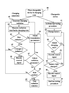
Fig. 5 is a block diagram illustrating a possible charging session according
to
some embodiments. The charging session is initiated in step 50 by placing a
chargeable
device inside the housing of a charging device of this application, as
described
hereinabove. Typically, the chargeable device is placed in a predefined
charging zone
inside the housing, or slid thereto by guiding means provided in the housing,
as
described hereinabove. Next, in step 61, the charging device is activated and
RF
radiation is transmitted from its antenna arrangement towards the charging
zone. The
device to be charged detects the RF radiation generated by the charging device
and in
CA 02875179 2014-11-28
WO 2013/179284
PCT/1L2013/050456
- 27 -
step 51 the device activates its harvesting system to charge its battery and
in step 52
starts the charging process.
In step 62 the charging device measure the RF radiation inside the housing of
the device, and in step 63 it is determined based on the measured RF radiation
if the
MEV is properly positioned inside the housing to efficiently transfer maximal
RF
charging energy to the device. If it is determined in step 63 that the RF
energy is not
efficiently transferred to the device, then in step 64 the transmission
parameters are
adjusted to move and/or rotate the MEV inside the housing to improve the
charging
process and the control is passed back to step 61. The RF radiation
measurement and
to adjustment of steps 61 to 64 may be repeated a number of times until it
is determined in
step in step 63 that the RF radiation energy is efficiently delivered to the
device being
charged and the efficiency of the charging session is improved.
The device being charged may be configured to determine from time to time (or
periodically) the efficiency of the charging process, as indicated by step 53.
If it is
determined in the device that adjustments are needed to improve the charging
process,
then the control is passed to step 54 to encode control signals by inducing
changes in
the RF radiation inside the housing (e.g., using antenna cutoff circuitry
533). Otherwise,
if it is determined in step 53 that the charging process is proper, then the
control is
passed back to step 52 to proceed with the charging process as is. In step 55
it is
determined if the battery of the device being charged is fully charged. If
further
charging is needed then the control is passed back to step 52 to proceed with
the
charging process, otherwise, if it is determined that the battery is
sufficiently charged
then in step 56 a respective control signal is encoded by inducing changes in
the RF
radiation to indicated to the charging device that the charging process is to
be ended, the
control is passed then to step 57 wherein the device stops the operation of
the harvesting
system and terminates the charging.
If it is determined at the charging device in step 63 that the RF radiation
energy
is efficiently transferred to the device being charged the control is passed
to step 65
wherein it is checked if there are variations in the intensity of the RF
radiation inside the
housing that may be induced by the controller of the device being charged. If
such
changes are not detected, the control is passed to step 61 to proceed with the
charging
session. If changes in the RF radiation are detected in step 65, then in step
66 data (e.g.,
CA 02875179 2014-11-28
WO 2013/179284
PCT/1L2013/050456
- 28 -
control signals) decoded by the charging device inducing the changes are
decoded and
analyzed. In step 67 it is determined if control signals decoded in the
detected changes
indicate that adjustments in the RF radiation are needed. If such adjustments
are needed,
then the control is passed to step 64 to carry out any needed adjustments to
improve the
efficiency of the charging process, as described herein above.
In case decoded signals do not indicate that adjustments are needed, then in
step
68 if the decoded signal indicates that the device instructs the device to
terminate the
charging session, then control is passed to step 69, wherein the charging
device stops
the emission of the RF radiation and terminates the charging session.
Otherwise, if no
to actions are to be carried out (e.g., the detected changes in the RF
radiation were used to
transfer data to the charging device, or the decoding failed to recognize
control
signals/data in the induced changes), then the control is passed back to step
61 to
proceed with the charging session.
EXAMPLES
In the following example various configuration of the inner cavity of the
housing of the charging device were tested using computer simulation software
(CST
3D electromagnetic field simulations). The dimensions of the inner cavity in
the
following examples, are as follows:
In Examples 1, 2 and 3: Length: 70 to 100 mm;
Width/diameter: 70 to 90 mm; and
In Examples 3: Height: 10 to 30 mm.
In all Examples, a distance between the antenna arrangement plane and the
MEV / charging zone (depending on the frequency of emitted radiation for a
given
geometry of the cavity) is about 20-50 mm.
Example 1 (cylindrical inner cavity)
This experiment tested the efficiency of RF radiation delivery in a
cylindrically
shaped housing structure 6h. Fig. 6A schematically illustrates the experiment
setup,
wherein transmitting antenna 6-1 and receiving antenna 6-2, positioned inside
the
housing 6h were used to simulate a charging process. RF radiation power of
1Watts
emitted by the transmitting antenna 6-1 is received by the receiving antenna 6-
2
CA 02875179 2014-11-28
WO 2013/179284
PCT/1L2013/050456
- 29 -
configured to measure the intensity of the RF radiation. The results shown in
Fig. 6B
reflect the ratio of the measured RF radiation power and the total RF
transmission
power transmitted by the transmitting antenna 6-1.
As seen in Fig. 6B the power loses in this experiment are between 0 to -0.05
dB
in the 2.37 to 2.43 GHz frequency range (90-100%).
Example 2 (conical housing)
In this experiment a tapering housing (frusto-conical) configuration was
tested.
The experiment setup and the measured results are shown in Figs. 7A and 7B
respectively. As in Example 1, a transmitting antenna 7-1 and a receiving
antenna 7-2,
to were used to simulate a charging process inside the tapered housing
structure 7h. As
seen in Fig. 7B, the power loses in this experiment are between 0 to -0.05 dB
in the 2.44
to 2.47 GHz frequency range.
Example 3 (rectangular housing)
In this experiment a rectangular housing configuration was tested. The
experiment setup and the measured results are shown in Figs. 8A and 8B
respectively.
As in the previous examples, a transmitting antenna 8-1 and a receiving
antenna 8-2,
were used to simulate a charging process inside the rectangular housing
structure 8h.
Fig. 8B shows the simulation results obtained to test the RF energy
transmission
between the transmitting antenna 8-1 and the receiving antenna 8-2
It should be clear that the description of the variations and attached figures
set
forth in this specification serves only for a better understanding of the
invention,
without limiting its scope. It should also be clear that a person skilled in
the art, after
reading the present specification could make adjustments or amendments to the
attached
Figures and above described variations that would still be covered by the
present
invention.
Although various features of the disclosure may be described in the context of
a
single embodiment, the features may also be provided separately or in any
suitable
combination. Conversely, although the disclosure may be described herein in
the
context of separate embodiments for clarity, the disclosure may also be
implemented in
a single embodiment. Furthermore, it should be understood that the disclosure
may be
carried out or practiced in various ways, and that the disclosure may be
implemented in
CA 02875179 2014-11-28
WO 2013/179284 PCT/1L2013/050456
- 30 -
embodiments other than the exemplary ones described herein below. The
descriptions,
examples and materials presented in the description, as well as in the claims,
should not
be construed as limiting, but rather as illustrative.