Note: Descriptions are shown in the official language in which they were submitted.
CA 02876396 2014-12-11
WO 2013/191847 PCT/US2013/042247
1
ULTRASONIC TESTING DEVICE AND METHOD OF ASSEMBLY
TECHNICAL FIELD
[0101] The present disclosure relates generally to ultrasonic devices used for
non-
destructive testing and more particularly to ultrasonic testing devices having
a conical
array of separate transducer elements with gaps therebetween and methods of
assembly
thereof
BACKGROUND OF THE INVENTION
[01021 Non-destructive testing such as ultrasonic testing may be used to
inspect
various types of materials and components. Specifically, ultrasonic testing is
a suitable
method for finding internal flaws and/or material characteristics such as
thickness and the
like in most types of sound conducting materials. Such sound conducting
materials
include most metals and other types of substantially rigid materials.
Generally described,
such flaws or characteristics may be detected based upon changes in the
reflection of
sound waves on a boundary surface of the component with a generally high
degree of
accuracy.
[0103] Ultrasonic testing of, for example, tubes or axles with bores therein
may
require the use of a conical array to test under a certain angle of incidence.
In creating
the conical array, a large number of transducer elements may be positioned
about the
CA 02876396 2014-12-11
WO 2013/191847 PCT/US2013/042247
circumference so as to ensure complete coverage in the direction of rotation.
Moreover,
the ability to phase requires a couple of transducer elements with a width in
range of a
given wavelength. To position the transducer elements, however, may be time
consuming given the need for manually positioning and attaching the elements
thereon.
Moreover, although a substrate material may be used to contact a large number
of
elements in a linear array, such a substrate has not been capable of
accommodating the
configuration of a conical array.
[0104] There is thus a desire for an improved ultrasonic testing device using
a
conical array and a method of assembling the same. Preferably such a conical
array can
accommodate a large number of transducer elements with the use of a flexible
printed
circuit substrate material while avoiding the time and expense required with
manual
assembly.
SUMMARY OF THE INVENTION
[0105] In one exemplary embodiment, an ultrasonic testing device is provided.
The ultrasonic testing device may include a conical backing and an ultrasonic
transducer
assembly positioned on the conical backing. The ultrasonic transducer assembly
may
include a printed circuit substrate with a number of separate transducer
elements.
[0106] In a further exemplary embodiment, a method of assembling an ultrasonic
testing device is provided. The method may include the steps of attaching at
least one
transducer to a printed circuit substrate, arranging a number of separate
transducer
elements on the printed circuit substrate, attaching the printed circuit
substrate to a
2
CA 02876396 2014-12-11
WO 2013/191847 PCT/US2013/042247
backing, and folding the separate transducer elements over the backing into a
conical
array.
[0107] In a further exemplary embodiment, an ultrasonic testing device is
provided. The ultrasonic testing device may include a backing configured as a
conical
array, a printed circuit substrate positioned on the backing, and means for
producing a
plurality of separated ultrasound waves attached to the printed circuit
substrate.
[0108] These and other features and improvements of the present disclosure
will
become apparent to one of ordinary skill in the art upon review of the
following detailed
description when taken in conjunction with the several drawings and the
appended
claims.
BRIEF DESCRIPTION OF THE DRAWINGS
[0109] Fig. 1 is a schematic diagram showing an ultrasonic device configured
as a
conical array.
[0110] Fig. 2 is a side plan view of the ultrasonic device of Fig. 1.
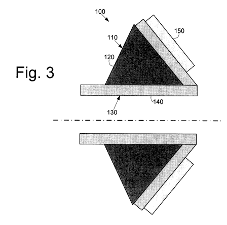
[0111] Fig. 3 is a schematic diagram of an ultrasonic device configured as a
conical array as may be described herein.
[0112] Fig. 4 is a schematic view of an ultrasound transducer assembly as may
be
used with the ultrasonic device of Fig. 3 before the separation cuts.
[0113] Fig. 5 is a schematic view of the ultrasonic transducer assembly as may
be
used with the ultrasonic device of Fig. 3 after the separation cuts.
3
CA 02876396 2014-12-11
WO 2013/191847 PCT/US2013/042247
[0114] Fig. 6 is a schematic plan view of the conical array of Fig. 2 with the
ultrasonic transducer assembly.
[0115] Fig. 7 is a flow chart of the assembly steps herein.
DETAILED DESCRIPTION
[0116] Referring now to the drawings, in which like numerals refer to like
elements throughout the several views, Figs. 1 and 2 show an ultrasonic
testing device
10. The ultrasonic testing device 10 may be configured as a conical array 15.
The
conical array 15 includes a backing 20 with a substantially conical shape. The
ultrasonic
testing device 10 further includes a number of transducers 25. The transducers
25 may be
positioned about the backing 20 of the conical array 15. The transducers 25
are generally
positioned and glued manually to the backing 20. The use of the conical array
15 allows
sound wave propagation by the transducers 25 at a desired angle of incidence.
The
ultrasonic testing device 10 may be inserted within a tube 30 for testing the
walls thereof
in a manner similar to that described above.
[0117] Fig. 3 shows an example of an ultrasonic testing device 100 as
described
herein. The ultrasonic testing device 100 may be configured as a conical array
110. The
conical array 110 may include a backing 120 with a substantially conical
shape. The
conical backing 120 may be made out of any type of material that does not
interfere with
the ultrasonic waves produced herein. The ultrasonic testing device 100 and
the conical
backing 120 may have any size. Other components and other configurations may
be used
herein.
4
CA 02876396 2014-12-11
WO 2013/191847 PCT/US2013/042247
[0118] The ultrasonic testing device 100 also may include an ultrasonic
transducer assembly 130. The ultrasonic transducer assembly 130 may include a
printed
circuit substrate 140 for positioning on the conical backing 120. The
substrate 140 may
be any type of thin film, flexible, printed circuit material such as, by way
of example and
not by limitation, a polyimide film, an electrodeposited copper foil, and the
like. Non-
metallic materials also may be used. A transducer 150 may be attached to the
printed
circuit substrate 140. The transducer 150 may be any type of piezoelectric
element that
converts electrical energy into sound waves. Moreover, a number of individual
transducers 150 may be applied to the printed circuit substrate 140. Other
components
and other configurations may be used herein.
[0119] In order to accommodate the shape of the conical array 110, the
transducer
150 of the ultrasonic transducer assembly 130 may have a number of separation
cuts 160
performed thereon. The separation cuts 160 may be made manually or in an
automated
fashion including laser cutting, die cutting, and other techniques. Once the
separation
cuts 160 are complete, a number of separate transducer elements 170 remain
with a gap
180 therebetween. The separation cuts 160 may continue beyond the transducer
150 and
into the printed circuit substrate 140. The separate transducer elements 170
with the gaps
180 therebetween may be expanded as is shown in Fig. 5. Any number of the
separation
cuts 160 and the separate transducer elements 170 may be used herein. The
separate
transducer elements 170 and the gaps 180 therebetween may have any size,
shape, or
configuration and may vary according to the size, shape, and configuration of
the conical
CA 02876396 2014-12-11
WO 2013/191847 PCT/US2013/042247
backing 120. The separation cuts 160 also may be applied to the printed
circuit substrate
140 with multiple transducers 150 thereon. Other components and other
configurations
may be used.
[0120] Each of the separate transducer elements 170 may be in communication
with a conductor 190. The conductors 190, in turn, may be in communication
with a
connector/soldering terminal 200 and the like. The
conductors 190 and the
connector/soldering terminal may be of conventional design. As is illustrated,
in Fig. 6,
the printed circuit substrate 140 with the separate transducer elements 170 of
the
ultrasonic transducer assembly 130 then may be attached to the backing 120 of
the
conical array 110. The separate transducer elements 170 may be folded to the
outside (or
the inside) of the conical backing 120 to form the conical configuration of
elements. The
ultrasonic transducer assembly 130 thus may accommodate the full circumference
of the
conical array 110. The
connector/soldering terminal 200 may be placed in
communication with a control unit in a conventional fashion.
[0121] Fig. 7 shows a flow chart of the high level steps that may be used to
create
the ultrasonic transducer device 100. The transducer 150 may be attached to
the printed
circuit substrate 140 in a first step 210. The separation cuts 160 may be
applied to the
transducer 150 and arranged to form the separate transducer elements 170 with
the gaps
180 therebetween in a second step 220. Alternatively, a number of individual
transducers
150 may be attached to the printed circuit substrate 140 in an alternative
first step 230.
The separation cuts 160 may be applied to the printed circuit substrate 140
and arranged
6
CA 02876396 2014-12-11
WO 2013/191847 PCT/US2013/042247
to form the separate transducer elements 170 with the gaps 180 therebetween in
an
alternative second step 240. In either example, the conductors 190 may be
coupled to the
separate transducer elements 170 in a third step 250. The printed circuit
substrate 140
may be attached to the backing 120 in a fourth step 260. The separate
transducer
elements 170 may be folded over the backing 120 in a fifth step 270 to
complete the
ultrasonic testing device 100. These steps may be performed in differing
order.
Additional steps may be used herein.
[01221 The ultrasonic testing device 100 thus provides the conical array 110
with
the ultrasonic transducer assembly 130 without having to individually position
and glue
or otherwise attach a number of the transducers 150. Rather, the separation
cuts 160
produce the separate transducer elements 170 with the gaps 180 therebetween so
as to
accommodate the shape of the conical array 110 by folding the separate
transducer
elements 170 about the conical backing 120. Similarly, the separation cuts 160
into the
printed circuit substrate 140 also may accommodate multiple individual
transducers 150.
The ultrasonic testing device 100 thus may be assembled as a phased array in
less time
and with less labor as compared to known ultrasonic devices typically used
with conical
arrays.
101231 It should be apparent that the foregoing relates only to certain
embodiments of the present invention. Numerous changes and modifications may
be
made herein by one of ordinary skill in the art without departing from the
general spirit
7
CA 02876396 2014-12-11
WO 2013/191847 PCT/US2013/042247
and scope of the invention herein as defined by the following claims and the
equivalents
thereof.
8