Note: Descriptions are shown in the official language in which they were submitted.
,
,
CA 02876696 2014-12-15
s
AUDIO INTERFACE SELF-ADAPTION DEVICE
FIELD
The present disclosure relates to an electronic technique field, and more
particularly relates to
an audio interface self-adaption device.
BACKGROUND
An audio interface (such as a headphone jack) of a conventional audio signal
sending device
(such as a mobile communication terminal) or an audio interface of a
conventional audio interface
receiving device (such as a headphone) is generally a four-section interface,
where a pin 1 and a
pin 2 are audio pins, namely a left-channel pin and a right-channel pin. As a
pin 3 and a pin 4 have
different functions in different audio interfaces, however, there are two
types of audio interfaces.
As one type, the pin 3 is a microphone pin (MIC pin) and the pin 4 is a ground
pin (GND pin). As
the other type, the pin 3 is a GND pin, and the pin 4 is a MIC pin.
As audio interfaces have the above different types, when an audio interface of
an audio signal
sending device (such as a mobile communication terminal) mismatches with an
audio interface of
an audio signal receiving device (such as a earphone or a headphone), the
audio signal sending
device and the audio signal receiving device can neither communicate with each
other via the MIC
pin of the audio interface, nor transmit audio signals between each other
normally using the audio
pins (a left-channel pin and a right channel-pin) of the audio interface.
Thus, an audio interface self-adaption device that can adapt to audio signal
send devices (such
as mobile communication terminals) having different audio interfaces is
required.
SUMMARY
The technical problem the present disclosure seeks to solve is to overcome at
least one
disadvantages in the related art, and to provide an audio interface self-
adaption device that can
adapt to audio signal send devices having different audio interfaces.
In order to solve the above problems, an audio interface self-adaption device
according to
embodiments of the present disclosure is provided. The device comprises an
audio interface
comprising a pin 1, a pin 2, a pin 3, and a pin 4; one of the pin 3 and the
pin 4 is a microphone pin
of the audio interface, and the other one of the pin 3 and the pin 4 is a
ground pin of the audio
1
CA 02876696 2014-12-15
interface. The device further comprises a first level comparison module, a
second level comparison
module, a PNP triode Tc, a power output terminal VBAT, a switching module, a
resistor R2a, and a
resistor R2b, where:
the first level comparison module comprises a NPN triode Ta, and the NPN
triode Ta
comprises a base connected to a first pin, an emitter connected to a second
pin, and a collector
connected to a base of the PNP triode Tc via the resistor R2a;
the second level comparison module comprises a NPN triode Tb, and the NPN
triode Tb
comprises a base connected to the second pin, an emitter connected to the
first pin, and a collector
connected to a signal input pin Sel of the switching module and connected to
the base of the PNP
triode Tc via the resistor R2b;
an emitter of the PNP triode Tc is connected to the power output terminal
VBAT, and a
collector of the PNP triode Tc is connected to a power input pin VCC of the
switching module;
the switching module is configured to connect one of the first input pin BOL
and the second
input pin B1H to the output pin of the switching module according to a level
of a signal received
by the signal input pin Sel;
an audio pin being the pin 1 and/or the pin 2 of the audio interface is
connected to a ground
wire; and
the first pin is one of the pin 3 and the pin 4 of the audio interface, and
the second pin is the
other one of the pin 3 and the pin 4 of the audio interface.
In some embodiments, the device further comprises a first unidirectional
conductive
component, a second unidirectional conductive component, and a resistor R4;
the audio pin is
connected to the pin 3 via the first unidirectional conductive component, and
the audio pin is
connected to the pin 4 via the second unidirectional conductive component; a
conducting direction
of the first unidirectional conductive component is from the audio pin to the
pin 3, and a
conducting direction of the second unidirectional conductive component is from
the audio pin to
the pin 4; and the pin 3 and the pin 4 of the audio interface are connected
via the resistor R4.
In some embodiments, the audio pin comprises the pin 1 and the pin 2 of the
audio interface;
the pin 1 is connected to the first unidirectional conductive component via a
first signal processing
module, the first unidirectional conductive component is connected to the pin
3, and the pin 1 is
connected to the pin 4 via the first signal processing module and the second
unidirectional
conductive component; and the pin 2 is connected to the first unidirectional
conductive component
2
. ,
CA 02876696 2014-12-15
..
. ,
via a second signal processing module, the first unidirectional conductive
component is connected
to the pin 3, and the pin 2 is connected to the pin 4 via the second signal
processing module and
the second unidirectional conductive component.
In some embodiments, the first unidirectional conductive component comprises
one selected
from a group consisting of: a diode, a triode, and a MOS; and the second
unidirectional conductive
component comprises one selected from a group consisting of: a diode, a
triode, and a MOS.
In some embodiments, the first signal processing module comprises at least one
selected from
a group consisting of: a resistor, a microphone, a transformer, a resistor,
and a comparator
connected in parallel, and a resistor and an operational amplifier connected
in parallel; and the
second signal processing module comprises at least one selected from a group
consisting of: a
resistor, a microphone, a transformer, a resistor and a comparator connected
in parallel, and a
resistor and an operational amplifier connected in parallel.
In some embodiments, the audio interface is a headphone plug or a headphone
jack.
Embodiments of the present disclosure provide an audio interface self-adaption
device. The
device comprises an audio interface; the audio interface comprises a pin 1, a
pin 2, a pin 3, and a
pin 4; one of the pin 3 and the pin 4 is a microphone pin of the audio
interface, and the other one
of the pin 3 and the pin 4 is a ground pin of the audio interface. The device
further comprises a
first level comparison module, a second level comparison module, a PNP triode
Tc, a power output
terminal VBAT, a switching module, a resistor R2a, and a resistor R2b; where:
the first level comparison module comprises a first reference voltage module
H1 and a
comparator Cl;
a positive electrode of the comparator Cl is connected to a second pin, a
negative electrode of
the first reference voltage module H1 is connected to a first pin, a positive
electrode of the first
reference voltage module H1 is connected to a negative electrode of the
comparator Cl, and an
output pin of the comparator Cl is connected to a base of the PNP triode Tc
via the resistor R2a;
the second level comparison module comprises a second reference voltage module
H2 and a
comparator C2;
a negative electrode of the comparator C2 is connected to the second pin, a
positive electrode
of the second reference voltage module H2 is connected to the first pin, a
negative electrode of the
second reference voltage module H2 is connected to the positive electrode of
the comparator C2,
and an output pin of the comparator C2 is connected to a signal input pin Sel
of the switching
3
. ,
CA 02876696 2014-12-15
module, and the output pin of the comparator C2 is connected to the base of
the PNP triode Tc via
the resistor R2b;
a first input pin BOL of the switching module is connected to the first pin, a
second input pin
B1H of the switching module is connected to the second pin, and an output pin
of the switching
module is connected to the ground;
the switching module is configured to connect one of the first input pin BOL
and the second
input pin B1H to the output pin of the switching module according to a level
of a signal received
by the signal input pin Sel;
an audio pin being the pin 1 and/or the pin 2 of the audio interface is
connected to a ground
wire; and
the first pin is one of the pin 3 and the pin 4 of the audio interface, and
the second pin is the
other one of the pin 3 and the pin 4 of the audio interface.
In some embodiments, the device further comprises a first unidirectional
conductive
component, a second unidirectional conductive component, and a resistor R4;
the audio pin is
connected to the pin 3 via the first unidirectional conductive component, and
the audio pin is
connected to the pin 4 via the second unidirectional conductive component; a
conducting direction
of the first unidirectional conductive component is from the audio pin to the
pin 3, and a
conducting direction of the second unidirectional conductive component is from
the audio pin to
the pin 4; and the pin 3 and the pin 4 of the audio interface are connected
via the resistor R4.
In some embodiments, the audio pin is the pin 1 and the pin 2 of the audio
interface; the pin 1
is connected to the first unidirectional conductive component via a first
signal processing module,
the first unidirectional conductive component is connected to the pin 3, and
the pin 1 is connected
to the pin 4 via the first signal processing module and the second
unidirectional conductive
component; and the pin 2 is connected to the first unidirectional conductive
component via a
second signal processing module, the first unidirectional conductive component
is connected to the
pin 3, and the pin 2 is connected to the pin 4 via the second signal
processing module and the
second unidirectional conductive component.
In some embodiments, the first unidirectional conductive component comprises
one selected
from a group consisting of: a diode, a triode, and a MOS; and the second
unidirectional conductive
component comprises one selected from a group consisting of: a diode, a
triode, and a MOS.
In some embodiments, the first signal processing module comprises at least one
selected from
4
CA 02876696 2014-12-15
. ,
a group consisting of: a resistor, a microphone, a transformer, a resistor and
a comparator
connected in parallel, and a resistor and an operational amplifier connected
in parallel; and the
second signal processing module comprises at least one selected from a group
consisting of: a
resistor, a microphone, a transformer, a resistor and a comparator connected
in parallel, and a
resistor and an operational amplifier connected in parallel.
In some embodiments, the audio interface is a headphone plug or a headphone
jack.
Embodiments of the present disclosure provide an audio interface self-adaption
device. The
device comprises an audio interface; the audio interface comprises a pin 1, a
pin 2, a pin 3, and a
pin 4; one of the pin 3 and the pin 4 is a microphone pin of the audio
interface, and the other one
of the pin 3 and the pin 4 is a ground pin of the audio interface. The device
further comprises a
first level comparison module, a second level comparison module, a PNP triode
Tc, a power output
terminal VBAT, a switching module, a resistor R2a, and a resistor R2b; where:
the first level comparison module comprises a NPN triode Ta;
the NPN triode Ta comprises a base connected to a first pin, an emitter
connected to a second
pin, and a collector connected to a base of the PNP triode Tc via the resistor
R2a;
the second level comparison module comprises a second reference voltage module
H2 and a
comparator C2;
a negative electrode of the comparator C2 is connected to the second pin, a
positive electrode
of the second reference voltage module H2 is connected to the first pin, a
negative electrode of the
second reference voltage module H2 is connected to a positive electrode of the
comparator C2, an
output pin of the comparator C2 is connected to a signal input pin Sel of the
switching module,
and the output pin of the comparator C2 is connected to the base of the PNP
triode Tc via the
resistor R2b;
an emitter of the PNP triode Tc is connected to the power output terminal
VBAT, and a
collector of the PNP triode Tc is connected to a power input pin VCC of the
switching module;
a first input pin BOL of the switching module is connected to the first pin, a
second input pin
B1H of the switching module is connected to the second pin, and an output pin
of the switching
module is connected to the ground;
the switching module is configured to connect one of the first input pin BOL
and the second
input pin B1H to the output pin of the switching module according to a level
of a signal received
by the signal input pin Sel;
5
CA 02876696 2014-12-15
=
an audio pin being the pin 1 and/or the pin 2 of the audio interface is
connected to a ground
wire; and
the first pin is one of the pin 3 and the pin 4 of the audio interface, and
the second pin is the
other one of the pin 3 and the pin 4 of the audio interface.
In some embodiments, the device further comprises a first unidirectional
conductive
component, a second unidirectional conductive component, and a resistor R4;
the audio pin is
connected to the pin 3 via the first unidirectional conductive component, and
the audio pin is
connected to the pin 4 via the second unidirectional conductive component; a
conducting direction
of the first unidirectional conductive component is from the audio pin to the
pin 3, and a
conducting direction of the second unidirectional conductive component is from
the audio pin to
the pin 4; and the pin 3 and the pin 4 of the audio interface are connected
via the resistor R4.
In some embodiments, the audio pin is the pin 1 and the pin 2 of the audio
interface; the pin 1
is connected to the first unidirectional conductive component via a first
signal processing module,
the first unidirectional conductive component is connected to the pin 3, and
the pin 1 is connected
to the pin 4 via the first signal processing module and the second
unidirectional conductive
component; and the pin 2 is connected to the first unidirectional conductive
component via a
second signal processing module, the first unidirectional conductive component
is connected to the
pin 3, and the pin 2 is connected to the pin 4 via the second signal
processing module and the
second unidirectional conductive component.
In some embodiments, the first unidirectional conductive component comprises
one selected
from a group consisting of: a diode, a triode, and a MOS; and the second
unidirectional conductive
component comprises one selected from a group consisting of: a diode, a
triode, and a MOS.
In some embodiments, the first signal processing module comprises at least one
selected from
a group consisting of: a resistor, a microphone, a transformer, a resistor and
a comparator
connected in parallel, and a resistor and an operational amplifier connected
in parallel; and the
second signal processing module comprises at least one selected from a group
consisting of: a
resistor, a microphone, a transformer, a resistor and a comparator connected
in parallel, and a
resistor and an operational amplifier connected in parallel.
In some embodiments, the audio interface is a headphone plug or a headphone
jack.
Embodiments of the present disclosure provide an audio interface self-adaption
device. The
device comprises an audio interface; the audio interface comprises a pin 1, a
pin 2, a pin 3, and a
6
, .
CA 02876696 2014-12-15
. .
pin 4; one of the pin 3 and the pin 4 is a microphone pin of the audio
interface, and the other one
of the pin 3 and the pin 4 is a ground pin of the audio interface. The device
further comprises a
first level comparison module, a second level comparison module, a PNP triode
Tc, a power output
terminal VBAT, a switching module, a resistor R2a, and a resistor R2b, where:
the first level comparison module comprises a first reference voltage module
H1 and a
comparator Cl;
a positive electrode of the comparator Cl is connected to a first pin, a
negative electrode of
the first reference voltage module H1 is connected to a second pin, a positive
electrode of the first
reference voltage module H1 is connected to a negative electrode of the
comparator Cl, and an
output pin of the comparator Cl is connected to a base of the PNP triode Tc
via the resistor R2a;
the second level comparison module comprises a NPN triode Tb;
the NPN triode Tb comprises a base connected to the first pin, an emitter
connected to the
second pin, and a collector connected to a signal input pin Sel of the
switching module and
connected to the base of the PNP triode Tc via the resistor R2b;
an emitter of the PNP triode Tc is connected to the power output terminal
VBAT, and a
collector of the PNP triode Tc is connected to a power input pin VCC of the
switching module;
a first input pin BOL of the switching module is connected to the second pin,
a second input
pin B1H of the switching module is connected to the first pin, and an output
pin of the switching
module is connected to the ground;
the switching module is configured to connect one of the first input pin BOL
and the second
input pin B1H to the output pin of the switching module according to a level
of a signal received
by the signal input pin Sel;
an audio pin being the pin 1 and/or the pin 2 of the audio interface is
connected to a ground
wire; and
the first pin is one of the pin 3 and the pin 4 of the audio interface, and
the second pin is the
other one of the pin 3 and the pin 4 of the audio interface.
In some embodiments, the device further comprises a first unidirectional
conductive
component, a second unidirectional conductive component, and a resistor R4;
the audio pin is
connected to the pin 3 via the first unidirectional conductive component, and
the audio pin is
connected to the pin 4 via the second unidirectional conductive component; a
conducting direction
of the first unidirectional conductive component is from the audio pin to the
pin 3, and a
7
. .
CA 02876696 2014-12-15
,
,
conducting direction of the second unidirectional conductive component is from
the audio pin to
the pin 4; and the pin 3 and the pin 4 of the audio interface are connected
via the resistor R4.
In some embodiments, the audio pin is the pin 1 and the pin 2 of the audio
interface; the pin 1
is connected to the first unidirectional conductive component via a first
signal processing module,
the first unidirectional conductive component is connected to the pin 3, and
the pin 1 is connected
to the pin 4 via the first signal processing module and the second
unidirectional conductive
component; and the pin 2 is connected to the first unidirectional conductive
component via a
second signal processing module, the first unidirectional conductive component
is connected to the
pin 3, and the pin 2 is connected to the pin 4 via the second signal
processing module and the
second unidirectional conductive component.
In some embodiments, the first unidirectional conductive component comprises
one selected
from a group consisting of: a diode, a triode, and a MOS; and the second
unidirectional conductive
component comprises one selected from a group consisting of: a diode, a
triode, and a MOS.
In some embodiments, the first signal processing module comprises at least one
selected from
a group consisting of: a resistor, a microphone, a transformer, a resistor and
a comparator
connected in parallel, and a resistor and an operational amplifier connected
in parallel; and the
second signal processing module comprises at least one selected from a group
consisting of: a
resistor, a microphone, a transformer, a resistor and a comparator connected
in parallel, and a
resistor and an operational amplifier connected in parallel.
In some embodiments, the audio interface is a headphone plug or a headphone
jack.
Embodiments of the present disclosure provide an audio interface self-adaption
device. The
device comprises an audio interface; the audio interface comprises a pin 1, a
pin 2, a pin 3 and a
pin 4; one of the pin 3 and the pin 4 is a microphone pin of the audio
interface, and the other one
of the pin 3 and the pin 4 is a ground pin of the audio interface. The device
further comprises a
first level comparison module, a second level comparison module, a power
output terminal VBAT,
a first switching module, a second switching module, and a resistor R2a, a
resistor R2b, a resistor
R3a, and a resistor R3b; where:
the first level comparison module comprises a NPN triode Ta, and the NPN
triode Ta of the
first level comparison module comprises a base connected to a first pin, an
emitter connected to a
second pin, and a collector connected to the power output terminal VBAT via
the resistor R2a and
the resistor R3a and connected to a signal input pin Sell of the first
switching module;
8
. .
CA 02876696 2014-12-15
=
. .
the second level comparison module comprises a NPN triode Tb, and the NPN
triode Tb of
the second level comparison module comprises a base connected to the second
pin, an emitter
connected to the first pin, and a collector connected to the power output
terminal VBAT via the
resistor R2b and the resistor R3b and connected to a signal input pin Se12 of
the second switching
module;
a first input pin BOL of the first switching module is connected to the first
pin, a first input pin
BOL of the second switching module is connected to the second pin; or, a
second input pin B1H of
the first switching module is connected to the second pin, and a second input
pin B1H of the
second switching module is connected to the first pin; and an output pin of
the first switching
module is connected to the ground, and an output pin of the second switching
module is connected
to the ground;
the first switching module is configured to connect the first input pin BOL of
the first
switching module to the output pin of the first switching module according to
a low level signal
received by the signal input pin Sell; the second switching module is
configured to connect the
first input pin BOL of the second switching module to the output pin of the
second switching
module according to a low level signal received by the signal input pin Se12;
the first switching
module is configured to connect the second input pin B1H of the first
switching module to the
output pin of the first switching module according to a high level signal
received by the signal
input pin Sell; and the second switching module is configured to connect the
second input pin
B1H of the second switching module to the output pin of the second switching
module according
to a high level signal received by the signal input pin Se12;
an audio pin being the pin 1 and/or the pin 2 of the audio interface is
connected to a ground
wire; and
the first pin is one of the pin 3 and the pin 4 of the audio interface, and
the second pin is the
other one of the pin 3 and the pin 4 of the audio interface.
In some embodiments, the device further comprises a first unidirectional
conductive
component, a second unidirectional conductive component, and a resistor R4;
the audio pin is
connected to the pin 3 via the first unidirectional conductive component, and
the audio pin is
connected to the pin 4 via the second unidirectional conductive component; a
conducting direction
of the first unidirectional conductive component is from the audio pin to the
pin 3, and a
conducting direction of the second unidirectional conductive component is from
the audio pin to
9
CA 02876696 2014-12-15
the pin 4; and the pin 3 and the pin 4 of the audio interface are connected
via the resistor R4.
In some embodiments, the audio pin is the pin 1 and the pin 2 of the audio
interface; the pin 1
is connected to the first unidirectional conductive component via a first
signal processing module,
the first unidirectional conductive component is connected to the pin 3, and
the pin 1 is connected
to the pin 4 via the first signal processing module and the second
unidirectional conductive
component; and the pin 2 is connected to the first unidirectional conductive
component via a
second signal processing module, the first unidirectional conductive component
is connected to the
pin 3, and the pin 2 is connected to the pin 4 via the second signal
processing module and the
second unidirectional conductive component.
In some embodiments, the first unidirectional conductive component comprises
one selected
from a group consisting of: a diode, a triode, and a MOS; and the second
unidirectional conductive
component comprises one selected from a group consisting of: a diode, a
triode, and a MOS.
In some embodiments, the first signal processing module comprises at least one
selected from
a group consisting of: a resistor, a microphone, a transformer, a resistor and
a comparator
connected in parallel, and a resistor and an operational amplifier connected
in parallel; and the
second signal processing module comprises at least one selected from a group
consisting of: a
resistor, a microphone, a transformer, a resistor and a comparator connected
in parallel, and a
resistor and an operational amplifier connected in parallel.
In some embodiments, the audio interface is a headphone plug or a headphone
jack.
Embodiments of the present disclosure provide an audio interface self-adaption
device. The
device comprises an audio interface; the audio interface comprises a pin 1, a
pin 2, a pin 3, and a
pin 4; one of the pin 3 and the pin 4 is a microphone pin of the audio
interface, and the other one
of the pin 3 and the pin 4 is a ground pin. The device further comprises a
first level comparison
module, a second level comparison module, a power output terminal VBAT, a
first switching
module, and a second switching module; where:
the first level comparison module comprises a first reference voltage module
H1 and a
comparator Cl;
a positive electrode of the comparator Cl is connected to a second pin; a
negative electrode of
the first reference voltage module H1 is connected to a first pin; a positive
electrode of the first
reference voltage module H1 is connected to a negative electrode of the
comparator C 1 ; and an
output pin of the comparator Cl is connected to a signal input pin Sell of the
first switching
. .
CA 02876696 2014-12-15
=
. .
module;
the second level comparison module comprises a second reference voltage module
H2 and a
comparator C2;
a negative electrode of the comparator C2 is connected to the second pin; a
positive electrode
of the second reference voltage module H2 is connected to the first pin; a
negative electrode of the
second reference voltage module H2 is connected to a positive electrode of the
comparator C2; and
an output pin of the comparator C2 is connected to a signal input pin Se12 of
the second switching
module;
a first input pin BOL of the first switching module is connected to the first
pin, a first input pin
BOL of the second switching module is connected to the second pin; or, a
second input pin B1H of
the first switching module is connected to the second pin, a second input pin
B1H of the second
switching module is connected to the first pin; and an output pin of the first
switching module is
connected to the ground, and an output pin of the second switching module is
connected to the
ground;
the first switching module is configured to connect the first input pin BOL of
the first
switching module to the output pin of the first switching module according to
a low level signal
received by the signal input pin Sell; the second switching module is
configured to connect the
first input pin BOL of the second switching module to the output pin of the
second switching
module according to a low level signal received by the signal input pin Se12;
the first switching
module is configured to connect the second input pin B1H of the first
switching module to the
output pin of the first switching module according to a high level signal
received by the signal
input pin Sell ; the second switching module is configured to connect the
second input pin B1H of
the second switching module to the output pin of the second switching module
according to a high
level signal received by the signal input pin Se12;
an audio pin being the pin 1 and/or the pin 2 of the audio interface is
connected to a ground
wire; and
the first pin is one of the pin 3 and the pin 4 of the audio interface, and
the second pin is the
other one of the pin 3 and the pin 4.
In some embodiments, the device further comprises a first unidirectional
conductive
component, a second unidirectional conductive component, and a resistor R4;
the audio pin is
connected to the pin 3 via the first unidirectional conductive component, and
the audio pin is
11
CA 02876696 2014-12-15
connected to the pin 4 via the second unidirectional conductive component; a
conducting direction
of the first unidirectional conductive component is from the audio pin to the
pin 3, and a
conducting direction of the second unidirectional conductive component is from
the audio pin to
the pin 4; and the pin 3 and the pin 4 of the audio interface are connected
via the resistor R4.
In some embodiments, the audio pin comprises the pin 1 and the pin 2 of the
audio interface;
the pin 1 is connected to the first unidirectional conductive component via a
first signal processing
module, the first unidirectional conductive component is connected to the pin
3, and the pin 1 is
connected to the pin 4 via the first signal processing module and the second
unidirectional
conductive component; and the pin 2 is connected to the first unidirectional
conductive component
via a second signal processing module, the first unidirectional conductive
component is connected
to the pin 3, and the pin 2 is connected to the pin 4 via the second signal
processing module and
the second unidirectional conductive component.
In some embodiments, the first unidirectional conductive component comprises
one selected
from a group consisting of: a diode, a triode, and a MOS; and he second
unidirectional conductive
component comprises one selected from a group consisting of: a diode, a
triode, and a MOS.
In some embodiments, the first signal processing module comprises at least one
selected from
a group consisting of: a resistor, a microphone, a transformer, a resistor and
a comparator
connected in parallel, and a resistor and an operational amplifier connected
in parallel; and the
second signal processing module comprises at least one selected from a group
consisting of: a
resistor, a microphone, a transformer, a resistor and a comparator connected
in parallel, and a
resistor and an operational amplifier connected in parallel.
In some embodiments, the audio interface is a headphone plug or a headphone
jack.
Embodiments of the present disclosure provide an audio interface self-adaption
device. The
device comprises an audio interface; the audio interface comprises a pin 1, a
pin 2, a pin 3, and a
pin 4; one of the pin 3 and the pin 4 is a microphone pin of the audio
interface, and the other one
of the pin 3 and the pin 4 is a ground pin of the audio interface. The device
further comprises a
first level comparison module, a second level comparison module, a power
output terminal VBAT,
a first switching module, a second switching module, a resistor R2a, and a
resistor R3a; where:
the first level comparison module comprises a NPN triode To;
the NPN triode Ta comprises a base connected to a first pin, an emitter
connected to a second
pin, and a collector connected to the power output terminal VBAT via the
resistor R2a and the
12
CA 02876696 2014-12-15
resistor R3a and connected to a signal input pin Sell of the first switching
module via the resistor
R2a;
the second level comparison module comprises a second reference voltage module
H2 and a
comparator C2;
a negative electrode of the comparator C2 is connected to the second pin; a
positive electrode
of the second reference voltage module H2 is connected to the first pin; a
negative electrode of the
second reference voltage module H2 is connected to a positive electrode of the
comparator C2; an
output pin of the comparator C2 is connected to a signal input pin Sel2 of the
second switching
module;
a first input pin BOL of the first switching module is connected to the first
pin, a first input pin
BOL of the second switching module is connected to the second pin; or, a
second input pin B1H of
the first switching module is connected to the second pin, a second input pin
B1H of the second
switching module is connected to the first pin; and an output pin of the first
switching module is
connected to the ground, and an output pin of the second switching module is
connected to the
ground;
the first switching module is configured to connect the first input pin BOL of
the first
switching module to the output pin of the first switching module according to
the a low level
signal received by the signal input pin Sell; the second switching module is
configured to connect
the first input pin BOL of the second switching module to the output pin of
the second switching
module according to a low level signal received by the signal input pin 5e12;
the first switching
module is configured to connect the second input pin B1H of the first
switching module to the
output pin of the first switching module according to a high level signal
received by the signal
input pin Sell; and the second switching module is configured to connect the
second input pin
B1H of the second switching module to the output pin of the second switching
module according
to a high level signal received by the signal input pin Se12;
an audio pin being the pin 1 and/or the pin 2 of the audio interface is
connected to a ground
wire, and
the first pin is one of the pin 3 and the pin 4 of the audio interface, and
the second pin is the
other one of the pin 3 and the pin 4.
In some embodiments, the device further comprises a first unidirectional
conductive
component, a second unidirectional conductive component, and a resistor R4;
the audio pin is
13
CA 02876696 2014-12-15
connected to the pin 3 via the first unidirectional conductive component, and
the audio pin is
connected to the pin 4 via the second unidirectional conductive component; a
conducting direction
of the first unidirectional conductive component is from the audio pin to the
pin 3, and a
conducting direction of the second unidirectional conductive component is from
the audio pin to
the pin 4; and the pin 3 and the pin 4 of the audio interface are connected
via the resistor R4.
In some embodiments, the audio pin is the pin 1 and the pin 2 of the audio
interface; the pin 1
is connected to the first unidirectional conductive component via a first
signal processing module,
the first unidirectional conductive component is connected to the pin 3, and
the pin 1 is connected
to the pin 4 via the first signal processing module and the second
unidirectional conductive
component; and the pin 2 is connected to the first unidirectional conductive
component via a
second signal processing module, the first unidirectional conductive component
is connected to the
pin 3, and the pin 2 is connected to the pin 4 via the second signal
processing module and the
second unidirectional conductive component.
In some embodiments, the first unidirectional conductive component comprises
one selected
from a group consisting of: a diode, a triode, and a MOS; and the second
unidirectional conductive
component comprises one selected from a group consisting of: a diode, a
triode, and a MOS.
In some embodiments, the first signal processing module comprises at least one
selected from
a group consisting of: a resistor, a microphone, a transformer, a resistor and
a comparator
connected in parallel, and a resistor and an operational amplifier connected
in parallel; and the
second signal processing module comprises at least one selected from a group
consisting of: a
resistor, a microphone, a transformer, a resistor and a comparator connected
in parallel, and a
resistor and an operational amplifier connected in parallel.
In some embodiments, the audio interface is a headphone plug or a headphone
jack.
Embodiments of the present disclosure provide an audio interface self-adaption
device. The
device comprises an audio interface; the audio interface comprising a pin 1, a
pin 2, a pin 3, and a
pin 4; one of the pin 3 and the pin 4 is a microphone pin of the audio
interface, and the other one
of the pin 3 and the pin 4 is a ground pin of the audio interface. The device
further comprises a
first level comparison module, a second level comparison module, a power
output terminal VBAT,
a first switching module, a second switching module, a resistor R2b, and a
resistor R3b; where:
the first level comparison module comprises a first reference voltage module
H1 and a
comparator Cl;
14
CA 02876696 2014-12-15
a positive electrode of the comparator C 1 is connected to a first pin; a
negative electrode of
the first reference voltage module H1 is connected to a second pin; a positive
electrode of the first
reference voltage module H1 is connected to a negative electrode of the
comparator Cl; an output
pin of the comparator Cl is connected to a signal input pin Sell of the first
switching module;
the second level comparison module comprises a NPN triode Tb;
the NPN triode Tb comprises a base connected to the first pin, an emitter
connected to the
second pin, and a collector connected to the power output terminal VBAT via
the resistor R2b and
the resistor R3b and connected to a signal input pin Se12 of the second
switching module via the
resistor R2b;
a first input pin BOL of the first switching module is connected to the first
pin, a first input pin
BOL of the second switching module is connected to the second pin; or, a
second input pin B1H of
the first switching module is connected to the second pin, a second input pin
B IH of the second
switching module is connected to the first pin; and an output pin of the first
switching module is
connected to the ground, and an output pin of the second switching module is
connected to the
ground;
the first switching module is configured to connect the first input pin BOL of
the first
switching module to the output pin of the first switching module according to
the a low level
signal received by the signal input pin Sell; the second switching module is
configured to connect
the first input pin BOL of the second switching module to the output pin of
the second switching
module according to a low level signal received by the signal input pin Se12;
the first switching
module is configured to connect the second input pin B1H of the first
switching module to the
output pin of the first switching module according to a high level signal
received by the signal
input pin Sell; the second switching module is configured to connect the
second input pin B1H of
the second switching module to the output pin of the second switching module
according to a high
level signal received by the signal input pin Se12;
an audio pin being the pin 1 and/or the pin 2 of the audio interface is
connected to a ground
wire; and
the first pin is one of the pin 3 and the pin 4 of the audio interface, and
the second pin is the
other one of the pin 3 and the pin 4.
In some embodiments, the device further comprises a first unidirectional
conductive
component, a second unidirectional conductive component, and a resistor R4;
the audio pin is
CA 02876696 2014-12-15
connected to the pin 3 via the first unidirectional conductive component, and
the audio pin is
connected to the pin 4 via the second unidirectional conductive component; a
conducting direction
of the first unidirectional conductive component is from the audio pin to the
pin 3, and a
conducting direction of the second unidirectional conductive component is from
the audio pin to
the pin 4; and the pin 3 and the pin 4 of the audio interface are connected
via the resistor R4.
In some embodiments, the audio pin comprises the pin 1 and the pin 2 of the
audio interface;
the pin 1 is connected to the first unidirectional conductive component via a
first signal processing
module, the first unidirectional conductive component is connected to the pin
3, and the pin 1 is
connected to the pin 4 via the first signal processing module and the second
unidirectional
conductive component; the pin 2 is connected to the first unidirectional
conductive component via
a second signal processing module, the first unidirectional conductive
component is connected to
the pin 3, and the pin 2 is connected to the pin 4 via the second signal
processing module and the
second unidirectional conductive component.
In some embodiments, the first unidirectional conductive component comprises
one selected
from a group consisting of: a diode, a triode, and a MOS; and the second
unidirectional conductive
component comprises one selected from a group consisting of: a diode, a
triode, and a MOS.
In some embodiments, the first signal processing module comprises at least one
selected from
a group consisting of: a resistor, a microphone, a transformer, a resistor and
a comparator
connected in parallel, and a resistor and an operational amplifier connected
in parallel; and the
second signal processing module comprises at least one selected from a group
consisting of: a
resistor, a microphone, a transformer, a resistor and a comparator connected
in parallel, and a
resistor and an operational amplifier connected in parallel.
In some embodiments, the audio interface is a headphone plug or a headphone
jack.
Embodiments of the present disclosure provide an audio interface self-adaption
device. The
device comprises an audio interface; the audio interface comprises a pin 1, a
pin 2, a pin 3, and a
pin 4; one of the pin 3 and the pin 4 is a microphone pin of the audio
interface, and the other one
of the pin 3 and the pin 4 is a ground pin of the audio interface. The device
further comprises a
level comparison module and an earthed switching module; where the level
comparison module is
configured to detect levels of the pin 3 and the pin 4 of the audio interface
and to output a control
instruction for controlling the earthed switching module according to the
detected levels; and the
earthed switching module is configured to connect a GND pin being the pin 3 or
the pin 4 of the
16
CA 02876696 2014-12-15
=
audio interface to the ground according to the control instruction.
In some embodiments, the level comparison module comprises a first level
comparison
module and a second level comparison module.
In some embodiments, the first level comparison module comprises a triode or a
comparator;
and the second level comparison module comprises a triode or a comparator.
In some embodiments, the earthed switching module comprises a switching
module, and the
switching module is configured to receive a control instruction output by the
first level comparison
module or the second level comparison module after the levels of the pin 3 and
the pin 4 of the
audio interface are detected by the first level comparison module or the
second level comparison
module.
In some embodiments, the switching module further comprises a delay switching
module
configured to delay powering on the switching module.
In some embodiments, the earthed switching module comprises a first switching
module
and/or a second switching module; the first switching module is configured to
receive a control
instruction output by the first level comparison module after the levels of
the pin 3 and the pin 4 of
the audio interface are detected by the first level comparison module; and the
second switching
module is configured to receive the control instruction output by the second
level comparison
module after the levels of the pin 3 and the pin 4 of the audio interface are
detected by the second
level comparison module.
In some embodiments, an audio pin being the pin 1 and/or the pin 2 of the
audio interface is
connected to a ground wire; the device further comprises a first
unidirectional conductive
component, a second unidirectional conductive component, and a resistor R4;
the audio pin is
connected to the pin 3 via the first unidirectional conductive component, and
the audio pin is
connected to the pin 4 via the second unidirectional conductive component; a
conducting direction
of the first unidirectional conductive component is from the audio pin to the
pin 3, and a
conducting direction of the second unidirectional conductive component is from
the audio pin to
the pin 4; and the pin 3 and the pin 4 of the audio interface are connected
via the resistor R4.
In some embodiments, the audio pin comprises the pin 1 and the pin 2 of the
audio interface;
the pin 1 is connected to the first unidirectional conductive component via a
first signal processing
module, the first unidirectional conductive component is connected to the pin
3, and the pin 1 is
connected to the pin 4 via the first signal processing module and the second
unidirectional
17
= .
CA 02876696 2014-12-15
. .
conductive component; and the pin 2 is connected to the first unidirectional
conductive component
via a second signal processing module, the first unidirectional conductive
component is connected
to the pin 3, and the pin 2 is connected to the pin 4 via the second signal
processing module and
the second unidirectional conductive component.
In some embodiments, the first unidirectional conductive component comprises
one selected
from a group consisting of: a diode, a triode, and a MOS; and the second
unidirectional conductive
component comprises one selected from a group consisting of: a diode, a
triode, and a MOS.
In some embodiments, the first signal processing module comprises at least one
selected from
a group consisting of: a resistor, a microphone, a transformer, a resistor and
a comparator
connected in parallel, and a resistor and an operational amplifier connected
in parallel; and the
second signal processing module comprises at least one selected from a group
consisting of: a
resistor, a microphone, a transformer, a resistor and a comparator connected
in parallel, and a
resistor and an operational amplifier connected in parallel.
In some embodiments, the audio interface is a headphone plug or a headphone
jack.
The audio interface self-adaption device according to embodiments of the
present disclosure
may adapt to audio signal sending devices having different audio interfaces
automatically at a
lower cost, and successfully pass a detection conducted by the audio signal
sending device when
an audio device connected to the audio interface self-adaption device is
detecting a MIC pin of the
audio interface (i.e. supplying an offset voltage to the MIC pin).
BRIEF DESCRIPTION OF THE DRAWINGS
Fig. 1 is a schematic view of an audio interface self-adaption device
according to a first
embodiment of the present disclosure;
Fig. 2 is a schematic view of an audio interface self-adaption device
according to a second
embodiment of the present disclosure;
Fig. 3 is a schematic view of an audio interface self-adaption device
according to a third
embodiment of the present disclosure;
Fig. 4 is a schematic view of an audio interface self-adaption device
according to a fourth
embodiment of the present disclosure;
Fig. 5 is a schematic view of an audio interface self-adaption device
according to a fifth
embodiment of the present disclosure;
18
CA 02876696 2014-12-15
Fig. 6 is a schematic view of an audio interface self-adaption device
according to a sixth
embodiment of the present disclosure;
Fig. 7 is a schematic view of an audio interface self-adaption device
according to a seventh
embodiment of the present disclosure;
Fig. 8 is a schematic view of an audio interface self-adaption device
according to an eighth
embodiment of the present disclosure;
Fig. 9 is a schematic view of an audio interface self-adaption device
according to a ninth
embodiment of the present disclosure;
Fig. 10 is a schematic view of an audio interface self-adaption device
according to a tenth
embodiment of the present disclosure;
Fig. 11 is a schematic view of an audio interface self-adaption device
according to an
eleventh embodiment of the present disclosure;
Fig. 12 is a schematic view of an audio interface self-adaption device
according to a twelfth
embodiment of the present disclosure;
Fig. 13 is a schematic view of an audio interface self-adaption device
according to a
thirteenth embodiment of the present disclosure;
Fig. 14 is a schematic view of an audio interface self-adaption device
according to a
fourteenth embodiment of the present disclosure;
Fig. 15 is a schematic view of an audio interface self-adaption device
according to a fifteenth
embodiment of the present disclosure;
Fig. 16 is a schematic view of an audio interface self-adaption device
according to a sixteenth
embodiment of the present disclosure;
Fig. 17 is a schematic view of an audio interface self-adaption device
according to a
seventeenth embodiment of the present disclosure; and
Fig. 18 is a schematic view of an audio interface self-adaption device
according to an
eighteenth embodiment of the present disclosure.
DETAILED DESCRIPTION
In the following, the present disclosure is described in detail with reference
to embodiments
in connection with the drawings.
An audio interface self-adaption device according to embodiments of the
present disclosure
19
4
=
CA 02876696 2014-12-15
,.
4 .
comprises an audio pin (such as a pin 1, a pin 2), a pin 3, and a pin 4. The
pin 1 and the pin 2 are
audio pins which may be a left-channel pin and a right-channel pin
respectively. According to
different audio interface standards, the pin 3 may be a MIC pin, and the pin 4
may be a GND pin;
or the pin 3 may be a GND pin, and the pin 4 may be a MIC pin.
The audio interface of the audio interface self-adaption device according to
embodiments of
the present disclosure can be any four-section headphone plug or four-section
headphone jack,
such as a headphone plug with a diameter of 3.5mm or 2.5mm or a headphone jack
with a
diameter of 3.5mm or 2.5mm.
If the audio interface of the audio interface self-adaption device according
to embodiments of
the present disclosure is a headphone plug, the audio interface of the audio
interface self-adaption
device according to embodiments of the present disclosure can be inserted into
a headphone jack
of an audio signal sending device (such as a smart phone) directly. If the
audio interface of the
audio interface self-adaption device of the audio interface self-adaption
device according to
embodiments of the present disclosure is a headphone jack, the audio interface
self-adaption
device can be connected to a headphone jack of a smart phone via a tieline
having two terminals
configured as headphone jacks.
Of course, the switching module of the audio interface self-adaption device
according to
embodiments of the present disclosure may be a switch such as a NX3L2267
switch, a
STG3682QTR switch, or an A0Z6184 switch.
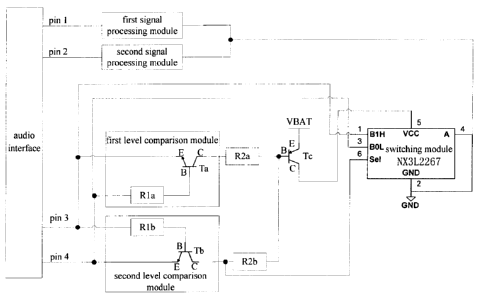
EMBODIMENT 1
Fig. 1 is a schematic view of an audio interface self-adaption device
according to a first
embodiment of the present disclosure. As shown in Fig.1, the audio interface
self-adaption device
of the embodiment comprises: an audio interface, a first level comparison
module, a second level
comparison module, a triode Tc, a power output terminal VBAT, a switching
module, a resistor
R2a, a resistor R2b, and so on.
The first level comparison module comprises a triode Ta, and the second level
comparison
module comprises a triode Tb.
The triode Ta is a NPN triode, the triode Tb is a NPN triode, and the triode
Tc is a PNP triode.
A base (B) of the triode Ta is connected to the pin 4, an emitter (E) of the
triode Ta is
connected to the pin 3, and a collector (C) of the triode Ta is connected to a
base (B) of the triode
=
CA 02876696 2014-12-15
..
. .
Tc via the resistor R2a.
Furthermore, the base (B) of the triode Ta may be connected to the pin 4 via a
resistor Rla.
A base (B) of the triode Tb is connected to the pin 3, an emitter (E) of the
triode Tb is
connected to the pin 4, and a collector (C) of the triode Tb is connected to a
signal input pin (Set)
of the switching module, and the collector (C) of the triode Tb is connected
to the base (B) of the
triode Tc via the resistor R2b.
Moreover, the base (B) of the triode Tb and the pin 3 may be connected via a
resistor Rib.
Each of the resistor R 1 a, the resistor R2a, the resistor Rib, and the
resistor R2b has a
resistance from 11(S2 to 1Ma
An emitter (E) of the triode Tc is connected to the power output terminal
VBAT, and a
collector (C) of the triode Tc is connected to a power input pin (VCC) of the
switching module.
If an ordinary battery is used as the power, a voltage output by the power is
generally from
2.7V to 4.2V.
A BOL pin (may be called a first input pin) of the switching module is
connected to the pin 4
of the audio interface, a Bill pin (may be called a second input pin) of the
switching module is
connected to the pin 3 of the audio interface, a ground pin (GND pin) of the
switching module is
connected to the ground, and a pin A (may be called an output pin) of the
switching module is
connected to the ground and to the pin 1 and the pin 2 of the audio interface.
Furthermore, the pin 1 of the audio interface may be connected to a ground
wire via a first
signal processing module, and the pin 2 of the audio interface may be
connected to the ground
wire via a second signal processing module.
Each of the first signal processing module and the second signal processing
module may
comprise at least one selected from a group consisting of: a resistor, a
louder speaker, a
transformer, and a signal processing module comprising a resistor and a
comparator connected in
parallel.
In the embodiment, when a level V3 of the pin 3 is greater than a sum of a
level V4 of the pin
4 and a predetermined threshold Vg (i.e. V3> V4 Vg), the triode Ta is in an
OFF state, the triode
Tb is in an ON state, and the triode Tc is in an ON state. The VBAT supplies
power to the
switching module via the VCC and a low level signal is received by the Set pin
of the switching
module, which indicates the pin 3 is the MIC pin and the pin 4 is the GND pin.
When the level V4 of the pin 4 is greater than the sum of the level V3 of the
pin 3 and the
21
CA 02876696 2014-12-15
predetermined threshold Vg (i.e. V4> V3 Vg), the triode Ta is in an ON state,
the triode Tb is in an
OFF state, and the triode Tc is in an ON state. The VBAT supplies power to the
switching module
via the VCC and a high level signal is received by the Sel pin of the
switching module, which
indicates the pin 4 is the MIC pin and the pin 3 is the GND pin.
The predetermined threshold Vg is greater than or equal to 0. In the
embodiment, the
threshold Vg may be a breakover voltage of the triode Ta, such as 0.3V or
0.7V.
The "high level signal" refers to a signal whose level is higher than the
level of the above
"low level signal". Generally, the "low level signal" is a signal whose
voltage is lower than 0.7V,
while the "high level signal" is a signal whose voltage is higher than seventy
percent of a voltage
of the power, the definitions of which may also be applied to descriptions
hereinafter.
The switching module connects the B1H pin or the BOL pin to the pin A
according to a signal
received by the Sel pin, such that the pin 3 or the pin 4 of the audio
interface is connected to the
ground.
When a low level signal is received by the Sel pin of the switching module,
the switching
module connects the BOL pin to the pin A, i.e. the BOL pin/ the pin 4 of the
audio interface is
connected to the ground.
When a high level signal is received by the Sel pin of the switching module,
the switching
module connects the B1H pin to the pin A, i.e. the B1H pin/ the pin 3 of the
audio interface is
connected to the ground.
According to a basic principle of the present invention, various variations
may be made to the
embodiment described above, for example:
1) changing the connection between the pin 3 of the audio interface and other
components, and the
connection between the pin 4 of the audio interface and other components;
2) connecting the signal input pin (Sc!) of the switching module between the
resistor R2a and the
collector (C) of the triode Ta.
EMBODIMENT 2
Fig. 2 is a schematic view of an audio interface self-adaption device
according to a second
embodiment of the present disclosure. As shown in Fig.2, the differences
between the present
embodiment and the Embodiment 1 are as follows.
(1) The pin 1 is connected to the pin 3 of the audio interface via a device
having
22
CA 02876696 2014-12-15
,
. .
unidirectional conductivity (may be called a unidirectional conductive
component, such as a diode,
a triode, a MOS, and so on), the pin 1 is connected to the pin 4 of the audio
interface via a device
having unidirectional conductivity (may be called a unidirectional conductive
component, such as
a diode, a triode, a MOS, and so on), the pin 2 of the audio interface is
connected to the pin 3 of
the audio interface via a device having unidirectional conductivity (may be
called a unidirectional
conductive component such as a diode, a triode, a MOS, and so on), and the pin
2 of the audio
interface is connected to the pin 4 of the audio interface via a device having
unidirectional
conductivity (may be called a unidirectional conductive component such as a
diode, a triode, a
MOS, and so on).
For example, as shown in Fig. 2, the pin 1 is connected to the pin 3 of the
audio interface via
a first signal processing module (such as a transformer U1) and a diode D1,
and the pin 2 of the
audio interface is connected to the pin 3 of the audio interface via a second
signal processing
module (such as a resistor R3) and the diode Dl. The pin 1 is connected to the
pin 4 of the audio
interface via the first signal processing module (such as the transformer U1)
and a diode D2, and
the pin 2 is connected to the pin 4 of the audio interface via the second
signal processing module
(such as the resistor R3) and the diode D2.
(2) The pin 3 and the pin 4 of the audio interface are connected via a
resistor R4.
A resistance of the resistor R4 is greater than 1Ka and the resistance of the
resistor R4 in the
embodiment may be from 11(0 to 20Ka
In the embodiment with the above additional technical features, the audio
interface
self-adaption device can be connected to an audio signal sending device with
any type of audio
interface, and pass a detection conducted by the audio signal sending device
successfully.
EMBODIMENT 3
Fig. 3 is a schematic view of an audio interface self-adaption device
according to a third
embodiment of the present disclosure. As shown in Fig.3, the audio interface
self-adaption device
of the embodiment comprises: an audio interface, a first level comparison
module, a second level
comparison module, a triode Tc, a power output terminal VBAT, a switching
module, a resistor
R2a, a resistor R2b, and so on.
The first level comparison module comprises a first reference voltage module
H1 and a
comparator Cl.
23
CA 02876696 2014-12-15
The pin 3 is connected to a positive electrode of the comparator Cl. The pin 4
is connected to
a negative electrode of the comparator Cl via the first reference voltage
module H1, i.e. the pin 4
is connected to a negative electrode of the first reference voltage module H1,
and a positive
electrode of the first reference voltage module H1 is connected to the
negative electrode of the
comparator Cl.
In the embodiment, the first reference voltage module H1 may be a power, and
the power has
a positive electrode being the positive electrode of the first reference
voltage module H1 and a
negative electrode being the negative electrode of the first reference voltage
module Hi. The
voltage provided by the first reference voltage module H1 is a predetermined
threshold Vg.
In other embodiments of the present disclosure, the first reference voltage
module H1 may be
a component which can supply a reference voltage (the threshold voltage) such
as a diode
connected to the power.
An output pin of the comparator Cl is connected to the base (B) of the triode
Tc via the
resistor R2a.
The second level comparison module comprises a second reference voltage module
H2 and a
comparator C2.
The pin 3 is connected to a negative electrode of the comparator C2. The pin 4
is connected to
a positive electrode of the comparator C2 via the second reference voltage
module H2, i.e. the pin
4 is connected to a positive electrode of the second reference voltage module
H2, and a negative
electrode of the second reference voltage module H2 is connected to the
positive electrode of the
comparator C2.
In the embodiment, the second reference voltage module H2 may be a power, and
the power
has a positive electrode being the positive electrode of the second reference
voltage module 112
and a negative electrode being the negative electrode of the second reference
voltage module H2.
The voltage provided by the second reference voltage module H2 is the
predetermined threshold
Vg.
In other embodiments of the present disclosure, the second reference voltage
module H2 may
be a component which can supply a reference voltage (the threshold voltage)
such as a diode
connected to the power.
An output pin of the comparator C2 is connected to a signal input pin (Sel) of
the switching
module, and the output pin of the comparator C2 is connected to the base (B)
of the triode Tc via
24
CA 02876696 2014-12-15
=
the resistor R2b.
Each of the resistor R2a and the resistor R2b has a resistance from 11(S2 to
1M1.
A B1H pin of the switching module is connected to the pin 3 of the audio
interface, a BOL pin
of the switching module is connected to the pin 4 of the audio interface, a
ground pin (GND pin)
of the switching module is connected to the ground (GND pin), and a pin A of
the switching
module is connected to the ground, and the pin A is connected to the pin 1 and
the pin 2 of the
audio interface.
Furthermore, the pin 1 of the audio interface may be connected to a ground
wire via a first
signal processing module, and the pin 2 of the audio interface may be
connected to the ground
wire via a second signal processing module.
Each of the first signal processing module and the second signal processing
module may
comprise at least one selected from a group consisting of: a resistor, a
louder speaker, a
transformer, and a signal processing module comprising a resistor and a
comparator connected in
parallel.
In the embodiment, when a level V3 of the pin 3 is greater than a sum of the
level V4 of the
pin 4 and a predetermined threshold Vg (i.e. V3> V4+Vg), a high level signal
is output by the
comparator Cl of the first level comparison module, a low level signal is
output by the comparator
C2 of the second level comparison module, the triode Tc is in an ON state, the
VBAT supplies
power to the switching module via the VCC, and a low level signal is received
by the Sel pin of
the switching module, which indicates the pin 3 is the MIC pin and the pin 4
is the GND pin.
When the level V4 of the pin 4 is greater than the sum of the level V3 of the
pin 3 and the
predetermined threshold Vg (i.e. V4> V3-f-Vg), a low level signal is output by
the comparator Cl of
the first level comparison module, a high level signal is output by the
comparator C2 of the second
level comparison module, the triode Tc is in an ON state, the VBAT supplies
power to the
switching module via the VCC, and a high level signal is received by the Sel
pin of the switching
module, which indicates the pin 4 is the MIC pin and the pin 3 is the GND pin.
The switching module connects the B1H pin or the BOL pin to the pin A
according to the
signal received by the Sel pin, such that the pin 3 or the pin 4 of the audio
interface is connected to
the ground.
When a low level signal is received by the Sel pin of the switching module,
the switching
module connects the BOL pin to the pin A, i.e. the BOL pin/ the pin 4 of the
audio interface is
CA 02876696 2014-12-15
connected to the ground.
When a high level signal is received by the Sel pin of the switching module,
the switching
module connects the B1H pin to the pin A, i.e. the B1H pin/ the pin 3 of the
audio interface is
connected to the ground.
According to the basic principle of the present invention, various variations
may be made to
the embodiment described above, for example:
1) changing the connection between the pin 3 of the audio interface and other
components and the
connection between the pin 4 of the audio interface and other components;
2) connecting the signal input pin (Sel) of the switching module between the
resistor R2a and the
output pin of comparator Cl.
EMBODIMENT 4
Fig. 4 is a schematic view of an audio interface self-adaption device
according to a fourth
embodiment of the present disclosure. As shown in Fig.4, the differences
between the present
embodiment and the Embodiment 3 are as follows.
(1) The pin 1 of the audio interface is connected to the pin 3 of the audio
interface via a
device having unidirectional conductivity (referred as a unidirectional
conductive component
hereinafter, such as a diode, a triode, a MOS, and so on), the pin 1 of the
audio interface is
connected to the pin 4 of the audio interface via a device having
unidirectional conductivity
(referred as a unidirectional conductive component hereinafter, such as a
diode, a triode, a MOS,
and so on), the pin 2 of the audio interface is connected to the pin 3 of the
audio interface via a
device having unidirectional conductivity (referred as a unidirectional
conductive component
hereinafter, such as a diode, a triode, a MOS, and so on), and the pin 2 of
the audio interface is
connected to the pin 4 of the audio interface via a device having
unidirectional conductivity
(referred as a unidirectional conductive component hereinafter, such as a
diode, a triode, a MOS,
and so on).
For example, as shown in Fig. 4, the pin 1 of the audio interface is connected
to the pin 3 of
the audio interface via a diode D1, the pin 2 of the audio interface is
connected to the pin 3 of the
audio interface via the diode D1, the pin 1 of the audio interface is
connected to the pin 4 of the
audio interface via a diode D2, and the pin 2 of the audio interface is
connected to the pin 4 of the
audio interface via the diode D2.
26
CA 02876696 2014-12-15
,
(2) The pin 3 and the pin 4 of the audio interface are connected via a
resistor R4.
The resistance of the resistor R4 is greater than 11(C2, and the resistance of
the resistor R4 of
the embodiment may be from 1K0 to 20KO.
In the embodiment with the above additional technical features, the audio
interface
self-adaption device can be connected to an audio signal sending device with
any type of audio
interface, and pass a detection conducted by the audio signal sending device
successfully.
EMBODIMENT 5
Fig. 5 is a schematic view of an audio interface self-adaption device
according to a fifth
embodiment of the present disclosure. As shown in Fig.5, the audio interface
self-adaption device
of the embodiment comprises: an audio interface, a first level comparison
module, a second level
comparison module, a PNP triode Tc, a power output terminal VBAT, a switching
module, a
resistor R2a, a resistor R2b, and so on.
The first level comparison module comprises a NPN triode Ta.
A base (B) of the triode Ta is connected to the pin 4, an emitter (E) of the
triode Ta is
connected to the pin 3, and a collector (C) of the triode Ta is connected to a
base (B) of the triode
Tc via the resistor R2a.
Furthermore, the base (B) of the triode Ta may be connected to the pin 4 via a
resistor Rla.
The second level comparison module comprises a second reference voltage module
H2 and a
comparator C2.
The pin 3 is connected to a negative electrode of the comparator C2. The pin 4
is connected to
a positive electrode of the comparator C2 via the second reference voltage
module 112, i.e. the pin
4 is connected to a positive electrode of the second reference voltage module
H2, and a negative
electrode of the second reference voltage module H2 is connected to the
positive electrode of the
comparator C2.
In the embodiment, the second reference voltage module H2 may be a power, and
the power
has a positive electrode being the positive electrode of the second reference
voltage module 142
and a negative electrode being the negative electrode of the second reference
voltage module 112.
The voltage provided by the second reference voltage module 112 is a
predetermined threshold Vg.
In other embodiments of the present disclosure, the second reference voltage
module H2 may
be a component which can supply a reference voltage (threshold voltage), such
as a diode
27
CA 02876696 2014-12-15
connected to a power.
An output pin of the comparator C2 is connected to a signal input pin (Se!) of
the switching
module, and the output pin of the comparator C2 is connected to the base (B)
of the triode Tc via
the resistor R2b.
Each of the resistor R2a and the resistor R2b has a resistance from 1KS2 to
IMO.
A B1H pin of the switching module is connected to the pin 3 of the audio
interface, a BOL pin
of the switching module is connected to the pin 4 of the audio interface, a
ground pin (GND pin)
of the switching module is connected to the ground, and a pin A of the
switching module is
connected to the ground, and the pin A of the switching module is connected to
the pin 1 and the
pin 2 of the audio interface.
Furthermore, the pin 1 of the audio interface may be connected to a ground
wire via a first
signal processing module, and the pin 2 of the audio interface may be
connected to the ground
wire via a second signal processing module.
Each of the first signal processing module and the second signal processing
module may
comprise at least one selected from a group consisting of: a resistor, a
louder speaker, a
transformer, and a signal processing module comprising a resistor and a
comparator connected in
parallel.
In the embodiment, when a level V3 of the pin 3 is greater than a sum of the
level V4 of the
pin 4 and a threshold Vg (i.e. V3> V4+Vg), the triode Ta is in an OFF state, a
low level signal is
output by the comparator C2 of the second level comparison module, the triode
Tc is in an ON
state, the VBAT supplies power to the switching module via the VCC, and a low
level signal is
received by the Sel pin of the switching module, which indicates the pin 3 is
the MIC pin and the
pin 4 is the GND pin.
When the level V4 of the pin 4 is greater than the sum of the level V3 of the
pin 3 and the
threshold Vg (i.e. V4> V3 Vg), the triodes Ta is in an ON state, a high level
signal is output by the
comparator C2 of the second level comparison module, the triodes Tc is in an
ON state, the VBAT
supplies power to the switching module via the VCC, and a high level signal is
received by the Sel
pin of the switching module, which indicates the pin 4 is the MIC pin and the
pin 3 is the GND
pin.
The threshold Vg is greater than or equal to 0. In the embodiment, the
threshold Vg may be a
breakover voltage of the triode Ta, such as 0.3V or 0.7V.
28
CA 02876696 2014-12-15
The switching module connects the B1H pin or the BOL pin to the pin A
according to the
signal received by the Sel pin, such that the pin 3 or the pin 4 of the audio
interface is connected to
the ground.
When a low level signal is received by the Sel pin of the switching module,
the switching
module connects the BOL pin to the pin A, i.e. the BOL pin/ the pin 4 of the
audio interface is
connected to the ground.
When a high level signal is received by the Sel pin of the switching module,
the switching
module connects the B1H pin to the pin A, i.e. the B1H pin/ the pin 3 of the
audio interface is
connected to the ground.
According to the basic principle of the present invention, various variations
may be made to
the embodiment described above, for example:
1) changing the connection between the pin 3 of the audio interface and other
components and the
connection between the pin 4 of the audio interface and other components.
2) connecting the signal input pin (Se!) of the switching module is between
the resistor R2a and
the collector (C) of the triode Ta.
EMBODIMENT 6
Fig. 6 is a schematic view of an audio interface self-adaption device
according to a sixth
embodiment of the present disclosure. As shown in Fig.6, the differences
between the sixth
embodiment and the fifth embodiment are as follows.
(1) The pin 1 of the audio interface is connected to the pin 3 of the audio
interface via a
device having unidirectional conductivity (referred as a unidirectional
conductive component
hereinafter, such as a diode, a triode, a MOS, and so on), the pin 1 of the
audio interface is
connected to the pin 4 of the audio interface via a device having
unidirectional conductivity
(referred as a unidirectional conductive component hereinafter, such as a
diode, a triode, a MOS,
and so on), the pin 2 of the audio interface is connected to the pin 3 of the
audio interface via a
device having unidirectional conductivity (referred as a unidirectional
conductive component
hereinafter, such as a diode, a triode, a MOS, and so on), and the pin 2 of
the audio interface is
connected to the pin 4 of the audio interface via a device having
unidirectional conductivity
(referred as a unidirectional conductive component hereinafter, such as a
diode, a triode, a MOS,
and so on).
29
CA 02876696 2014-12-15
For example, as shown in Fig. 6, the pin 1 of the audio interface is connected
to the pin 3 of
the audio interface via a diode D1, the pin 2 of the audio interface is
connected to the pin 3 of the
audio interface via the diode D1, the pin 1 of the audio interface is
connected to the pin 4 of the
audio interface via a diode D2, and the pin 2 of the audio interface is
connected to the pin 4 of the
audio interface via the diode D2.
(2) The pin 3 and the pin 4 of the audio interface are connected via a
resistor R4.
The resistance of the resistor R4 is greater than 11¶2, and the resistance of
the resistor R4 in
the embodiment may be from 1K0 to 20Ka
In the embodiment with the above additional technical features, the audio
interface
self-adaption device can be connected to an audio signal sending device with
any type of audio
interface, and pass a detection conducted by the audio signal sending device
successfully.
EMBODIMENT 7
Fig. 7 is a schematic view of an audio interface self-adaption device
according to a seventh
embodiment of the present disclosure. As shown in Fig.7, the audio interface
self-adaption device
of the embodiment comprises: an audio interface, a first level comparison
module, a second level
comparison module, a PNP triode Tc, a power output terminal VBAT, a switching
module, a
resistor R2a, a resistor R2b, and so on.
The first level comparison module comprises a first reference voltage module
H1 and a
comparator Cl.
The pin 3 is connected to a positive electrode of the comparator Cl. The pin 4
is connected to
a negative electrode of the comparator Cl via the first reference voltage
module H1, i.e. the pin 4
is connected to a negative electrode of the first reference voltage module H1,
and a positive
electrode of the first reference voltage module H1 is connected to the
negative electrode of the
comparator Cl.
In the embodiment, the first reference voltage module H1 may be a power, and
the power has
a positive electrode being the positive electrode of the first reference
voltage module H1 and a
negative electrode being the negative electrode of the first reference voltage
module Hi. The
voltage provided by the first reference voltage module H1 is a threshold Vg.
In other embodiments of the present disclosure, the first reference voltage
module H1 may be
a component which can supply a reference voltage (threshold voltage) such as a
diode connected
CA 02876696 2014-12-15
=
to the power.
An output pin of the comparator Cl is connected to a base (B) of the triode Tc
via the resistor
R2a.
The second level comparison module comprises a NPN triode Tb.
A base (B) of the triode Tb is connected to the pin 3, an emitter (E) of the
triode Tb is
connected to the pin 4, and a collector (C) of the triode Tb is connected to a
signal input pin (Sel)
of the switching module, and the collector (C) of the triode Tb is connected
to the base (B) of the
triode Tc via the resistor R2b.
Moreover, the base (B) of the triode Tb and the pin 3 may be connected via a
resistor Rib.
If an ordinary battery is used as the power, the voltage output by the power
is generally from
2.7V to 4.2V.
A B1H pin of the switching module is connected to the pin 3 of the audio
interface, a BOL pin
of the switching module is connected to the pin 4 of the audio interface, a
ground pin (GND pin)
of the switching module is connected to the ground, a pin A of the switching
module is connected
to the ground, and the pin A of the switching module is connected to the pin 1
and the pin 2 of the
audio interface.
Furthermore, the pin 1 of the audio interface may be connected to a ground
wire via a first
signal processing module, and the pin 2 of the audio interface may be
connected to the ground
wire via a second signal processing module.
Each of the first signal processing module and the second signal processing
module may
comprise at least one selected from a group consisting of: a resistor, a
louder speaker, a
transformer, and a signal processing module comprising a resistor and a
comparator connected in
parallel.
In the embodiment, when the level V3 of the pin 3 is greater than a sum of the
level V4 of the
pin 4 and a predetermined threshold Vg (i.e. V3> V4 Vg), a high level signal
is output by the
comparator C 1 of the first level comparison module, the triode Tb is in an ON
state, the triode Tc
is in an ON state, the VBAT supplies power to the switching module via the
VCC, and a low level
signal is received by the Set pin of the switching module, which indicates the
pin 3 is the MIC pin
and the pin 4 is the GND pin.
When the level V4 of the pin 4 is greater than the sum of the level V3 of the
pin 3 and the
predetermined threshold Vg (i.e. V4> V3+Vg), a low level signal is output by
the comparator Cl of
31
CA 02876696 2014-12-15
the first level comparison module, the triode Tb is in an OFF state, the
triode Tc is in an ON state,
the VBAT supplies power to the switching module via the VCC, and a high level
signal is received
by the Sel pin of the switching module, which indicates the pin 4 is the MIC
pin and the pin 3 is
the GND pin.
The above predetermined threshold Vg is greater than or equal to 0. In the
embodiment, the
threshold Vg may be a breakover voltage of the triode Ta, such as 0.3V or
0.7V.
The switching module connects the B1H pin or the BOL pin to the pin A
according to a signal
received by the Sel pin, such that the pin 3 or the pin 4 of the audio
interface is connected to the
ground.
When a low level signal is received by the Sel pin of the switching module,
the switching
module connects the BOL pin to the pin A, i.e. the BOL pin/ the pin 4 of the
audio interface is
connected to the ground.
When a high level signal is received by the Sel pin of the switching module,
the switching
module connects the B1H pin to the pin A, i.e. the B1H pin/ the pin 3 of the
audio interface is
connected to the ground.
According to the basic principle of the present invention, various variations
may be made to
the embodiment described above, for example:
1) changing the connection between the pin 3 of the audio interface and other
components and the
connection between the pin 4 of the audio interface and other components.
2) connecting the signal input pin (Sel) of the switching module between the
resistor R2a and the
output pin of the comparator Cl.
EMBODIMENT 8
Fig. 8 is a schematic view of an audio interface self-adaption device
according to an eighth
embodiment of the present disclosure. As shown in Fig.8, the differences
between the present
embodiment and Embodiment 7 are as follows.
(1) The pin 1 of the audio interface is connected to the pin 3 of the audio
interface via a
unidirectional conductive component (such as a diode, a triode, a MOS, and so
on), the pin 1 of the
audio interface is connected to the pin 4 of the audio interface via a
unidirectional conductive
component (such as a diode, a triode, a MOS, and so on), the pin 2 of the
audio interface is
connected to the pin 3 of the audio interface via a unidirectional conductive
component (such as a
32
CA 02876696 2014-12-15
diode, a triode, a MOS, and so on), and the pin 2 of the audio interface is
connected to the pin 4 of
the audio interface via a unidirectional conductive component (such as a
diode, a triode, a MOS,
and so on).
For example, as shown in Fig. 8, the pin 1 of the audio interface is connected
to the pin 3 of
the audio interface via a diode D1, the pin 2 of the audio interface is
connected to the pin 3 of the
audio interface via the diode D1, the pin 1 of the audio interface is
connected to the pin 4 of the
audio interface via a diode D2, and the pin 2 of the audio interface is
connected to the pin 4 of the
audio interface via the diode D2.
(2)The pin 3 and the pin 4 of the audio interface are connected via a resistor
R4.
The resistance of the resistor R4 is greater than 1KO, and the resistance of
the resistor R4 of
the embodiment may be from 1KS2 to 20Ka
In the embodiment with the above additional technical features, the audio
interface
self-adaption device can be connected to an audio signal sending device with
any type of audio
interface, and pass a detection conducted by the audio signal sending device
successfully.
EMBODIMENT 9
Fig. 9 is a schematic view of an audio interface self-adaption device
according to a ninth
embodiment of the present disclosure. As shown in Fig.9, the audio interface
self-adaption device
of the embodiment comprises: an audio interface, a first level comparison
module, a second level
comparison module, a power output terminal VBAT, a first switching module, a
second switching
module, and a resistor R2a, a resistor R2b, a resistor R3a, a resistor R3b,
and so on.
The first level comparison module comprises a triode Ta, and the second level
comparison
module comprises a triode Tb.
The triode Ta is a NPN triode, and the triode Ta is a NPN triode.
A base (B) of the triode Ta is connected to the pin 4, an emitter (E) of the
triode Ta is
connected to the pin 3, a collector (C) of the triode Ta is connected to the
power output terminal
VBAT via the resistor R2a and the resistor R3a, and the collector (C) of the
triode Ta is connected
to a signal input pin (Sell) of the first switching module via the resistor
R2a.
Furthermore, the base (B) of the triode Ta may be connected to the pin 4 via a
resistor Rla.
A base (B) of the triode Tb is connected to the pin 3, an emitter (E) of the
triode Tb is
connected to the pin 4, a collector (C) of the triode Tb is connected to the
power output terminal
33
CA 02876696 2014-12-15
VBAT via the resistor R2b and the resistor R3b, and the collector (C) of the
triode Tb is connected
to a signal input pin (Se12) of the second switching module via the resistor
R2b.
Moreover, the base (B) of the triode Tb and the pin 3 may be connected via a
resistor Rib.
Each of the resistor Rla, the resistor R2a, the resistor Rib , the resistor
R2b, the resistor R3a,
and the resistor R3b has a resistance from 11(S/ to 1MS2.
If an ordinary battery is used as the power, the voltage output by the power
is generally from
2.7 to 4.2V.
A BOL pin of the first switching module is connected to the pin 3 of the audio
interface, a
BOL pin of the second switching module is connected to the pin 4 of the audio
interface, a ground
pin (GND pin) of the first switching module is connected to the ground, a
ground pin (GND pin)
of the second switching module is connected to the ground, a pin A (may be
called an output pin)
of the first switching module is connected to the ground, and the pin A of the
first switching
module is connected to the pin 1 and the pin 2 of the audio interface, a pin A
(may be called an
output pin) of the second switching module is connected to the ground, and the
pin A of the second
switching module is connected to the pin 1 and the pin 2 of the audio
interface.
Furthermore, the pin 1 of the audio interface may be connected to a ground
wire via a first
signal processing module, and the pin 2 of the audio interface may be
connected to the ground
wire via a second signal processing module.
Each of the first signal processing module and the second signal processing
module may
comprise a resistor, a louder speaker, a transformer, and a signal processing
module comprising a
resistor and a comparator connected in parallel.
In the embodiment, when a level V3 of the pin 3 is greater than a sum of a
level V4 of the pin
4 and a predetermined threshold Vg (i.e. V3> V4+Vg), the triode Ta is in an
OFF state, the triode
Tb is in an ON state, a low level signal is received by the Se12 pin of the
second switching module,
which indicates the pin 3 is the MIC pin and the pin 4 is the GND pin.
When the level V4 of the pin 4 is greater than the sum of the level V3 of the
pin 3 and a
predetermined threshold Vg (i.e. V4> V3+Vg), the triode Ta is in an ON state,
the triode Tb is in an
OFF state, a low level signal is received by the Sell pin of the first
switching module, which
indicates the pin 4 is the MIC pin and the pin 3 is the GND pin.
The predetermined threshold Vg is greater than or equal to 0. In the
embodiment, the
threshold Vg may be a breakover voltage of the triode Ta, such as 0.3V or
0.7V.
34
CA 02876696 2014-12-15
The above "high level signal" is a signal whose level is higher than a level
of the above "low
level signal". Generally, the "low level signal" is a signal whose voltage is
lower than 0.7V, while
the "high level signal" is a signal whose voltage is higher than seventy
percent of the supply
voltage, the definitions of which may be applied to descriptions hereinafter.
The second switching module connects the BOL pin to the pin A according to a
low level
signal received by the Se12 pin, such that the pin 4 of the audio interface is
connected to the
ground.
When a low level signal is received by the Se12 pin of the second switching
module, the
second switching module connects the BOL pin to the pin A, i.e. the BOL pin/
the pin 4 of the audio
interface is connected to the ground.
The first switching module connects the BOL pin to the pin A according to a
low level signal
received by the Sell pin, such that the pin 3 of the audio interface is
connected to the ground.
When a low level signal is received by the Sell pin of the first switching
module, the first
switching module connects the BOL pin to the pin A, i.e. the BOL pin/ the pin
3 of the audio
interface is connected to the ground.
According to the basic principle of the present invention, various variations
may be made to
the embodiment described above, for example:
1) changing the connection between the pin 3 of the audio interface and other
components and the
connection between the pin 4 of the audio interface and other components;
2) connecting the pin 4 of the audio interface to the B1H instead of the BOL
of the first switching
module, and connecting the pin 3 of the audio interface to the B1H instead of
the BOL of the
second switching module.
EMBODIMENT 10
Fig. 10 is a schematic view of an audio interface self-adaption device
according to a tenth
embodiment of the present disclosure. As shown in Fig.10, the differences
between the present
embodiment and Embodiment 9 are as follows.
(1) The pin 1 of the audio interface is connected to the pin 3 of the audio
interface via a
device having unidirectional conductivity (referred as a unidirectional
conductive component
hereinafter, such as a diode, a triode, a MOS, and so on), the pin 1 of the
audio interface is
connected to the pin 4 of the audio interface via a device having
unidirectional conductivity
CA 02876696 2014-12-15
(referred as a unidirectional conductive component hereinafter, such as a
diode, a triode, a MOS,
and so on), the pin 2 of the audio interface is connected to the pin 3 of the
audio interface via a
device having unidirectional conductivity (referred as a unidirectional
conductive component
hereinafter, such as a diode, a triode, a MOS, and so on), and the pin 2 of
the audio interface is
connected to the pin 4 of the audio interface via a device having
unidirectional conductivity
(referred as a unidirectional conductive component hereinafter, such as a
diode, a triode, a MOS,
and so on).
For example, as shown in Fig. 10, the pin 1 of the audio interface is
connected to the pin 3 of
the audio interface via a first signal processing module (such as a
transformer U1) and a diode D1,
the pin 2 of the audio interface is connected to the pin 3 of the audio
interface via a second signal
processing module (such as a resistor R5) and the diode D1, the pin 1 of the
audio interface is
connected to the pin 4 of the audio interface via a first signal processing
module (such as the
transformer U1) and a diode D2, and the pin 2 of the audio interface is
connected to the pin 4 of
the audio interface via a second signal processing module (such as the
resistor R5) and the diode
D2.
(2) The pin 3 and the pin 4 of the audio interface are connected via a
resistor R4.
The resistance of the resistor R4 is greater than 11(fl, and the resistance of
the resistor R4 of
the embodiment may be from 11(0 to 20Ka
In the embodiment with the above additional technical features, the audio
interface
self-adaption device can be connected to an audio signal sending device with
any type of audio
interface, and pass a detection conducted by the audio signal sending device
successfully.
EMBODIMENT 11
Fig. 11 is a schematic view of an audio interface self-adaption device
according to an
eleventh embodiment of the present disclosure. As shown in Fig.11, the audio
interface
self-adaption device of the embodiment comprises: an audio interface, a first
level comparison
module, a second level comparison module, a power output terminal VBAT, a
first switching
module, a second switching module, and so on.
The first level comparison module comprises a first reference voltage module
H1 and a
comparator Cl.
The pin 3 is connected to a positive electrode of the comparator Cl. The pin 4
is connected to
36
=,
CA 02876696 2014-12-15
a negative electrode of the comparator Cl via the first reference voltage
module H1, i.e. the pin 4
is connected to a negative electrode of the first reference voltage module H1,
and a positive
electrode of the first reference voltage module 111 is connected to the
negative electrode of the
comparator Cl.
In the embodiment, the first reference voltage module H1 may be a power, and
the power has
a positive electrode being the positive electrode of the first reference
voltage module H1 and a
negative electrode being the negative electrode of the first reference voltage
module Hi. The
voltage provided by the first reference voltage module H1 is a threshold Vg.
In other embodiments of the present disclosure, the first reference voltage
module H1 may be
a component which can supply a reference voltage (threshold voltage) such as a
diode connected
to the power.
An output pin of the comparator C 1 is connected to a signal input pin (Sell)
of the first
switching module.
The second level comparison module comprises a second reference voltage module
H2 and a
comparator C2.
The pin 3 is connected to a negative electrode of the comparator C2. The pin 4
is connected to
a positive electrode of the comparator C2 via the second reference voltage
module H2, i.e. the pin
4 is connected to a positive electrode of the second reference voltage module
H2, and a negative
electrode of the second reference voltage module H2 is connected to the
positive electrode of the
comparator C2.
In the embodiment, the second reference voltage module H2 may be a power, and
the power
has a positive electrode being the positive electrode of the second reference
voltage module H2
and a negative electrode being the negative electrode of the second reference
voltage module H2.
The voltage provided by the second reference voltage module H2 is the
threshold Vg.
In other embodiments of the present disclosure, the second reference voltage
module H2 may
be a component which can supply a reference voltage (threshold voltage), such
as a diode
connected to a power.
An output pin of the comparator C2 is connected to a signal input pin (Se12)
of the second
switching module.
A BOL pin of the first switching module is connected to the pin 3 of the audio
interface, a
BOL pin of the second switching module is connected to the pin 4 of the audio
interface, a ground
37
CA 02876696 2014-12-15
pin (GND pin) of the first switching module is connected to the ground, a
ground pin (GND pin)
of the second switching module is connected to the ground, a pin A of the
first switching module is
connected to the ground, the pin A of the first switching module is connected
to the pin 1 and the
pin 2 of the audio interface respectively, a pin A of the second switching
module is connected to
the ground, and the pin A of the second switching module is connected to the
pin 1 and the pin 2 of
the audio interface respectively.
Furthermore, the pin 1 of the audio interface may be connected to a ground
wire via a first
signal processing module, and the pin 2 of the audio interface may be
connected to the ground
wire via a second signal processing module.
Each of the first signal processing module and the second signal processing
module may
comprise at least one selected from a group consisting of: a resistor, a
louder speaker, a
transformer, and a signal processing module comprising a resistor and a
comparator connected in
parallel.
In the embodiment, when a level V3 of the pin 3 is greater than a sum of a
level V4 of the pin
4 and a threshold Vg (i.e. V3> V4 Vg), a high level signal is output by the
comparator Cl of the
first switching module, a low level signal is output by the comparator C2 of
the second switching
module, a low level signal is received by the Se12 pin of the second switching
module, which
indicates the pin 3 is the MIC pin and the pin 4 is the GND pin.
When the level V4 of the pin 4 is greater than the sum of the level V3 of the
pin 3 and the
threshold Vg (i.e. V4> V3 Vg), a low level signal is output by the comparator
Cl of the first
switching module, a high level signal is output by the comparator C2 of the
second switching
module, a low level signal is received by the Sell pin of the first switching
module, which
indicates the pin 4 is the MIC pin and the pin 3 is the GND pin.
The first switching module connects the BOL pin to the pin A according to the
low level
signal received by the Sell pin, such that the pin 3 of the audio interface is
connected to the
ground.
When a low level signal is received by the Sell pin of the first switching
module, the first
switching module connects the BOL pin to the pin A, i.e. the BOL pin/ the pin
3 of the audio
interface is connected to the ground.
The second switching module connects the BOL pin to the pin A according to the
low level
signal received by the Se12 pin, such that the pin 4 of the audio interface is
connected to the
38
CA 02876696 2014-12-15
ground.
When a low level signal is received by the Sel2 pin of the second switching
module, the
second switching module connects the BOL pin to the pin A, i.e. the BOL pin/
the pin 4 of the audio
interface is connected to the ground.
According to the basic principle of the present invention, various variations
may be made to
the embodiment described above, for example:
1) changing the connection between the pin 3 of the audio interface and other
components and the
connection between the pin 4 of the audio interface and other components;
2) connecting the pin 3 of the audio interface to the B1H instead of BOL of
the first switching
module, and connecting the pin 4 of the audio interface to the B1H instead of
BOL of the second
switching module.
EMBODIMENT 12
Fig. 12 is a schematic view of an audio interface self-adaption device
according to a twelfth
embodiment of the present disclosure. As shown in Fig.12, the differences
between the present
embodiment and Embodiment 11 are as follows.
(1) The pin 1 of the audio interface is connected to the pin 3 of the audio
interface via a
unidirectional conductive component (such as a diode, a triode, a MOS, and so
on), the pin 1 of the
audio interface is connected to the pin 4 of the audio interface via a
unidirectional conductive
component (such as a diode, a triode, a MOS, and so on), the pin 2 of the
audio interface is
connected to the pin 3 of the audio interface via a unidirectional conductive
component (such as a
diode, a triode, a MOS, and so on), and the pin 2 of the audio interface is
connected to the pin 4 of
the audio interface via a unidirectional conductive component (such as a
diode, a triode, a MOS,
and so on).
For example, as shown in Fig. 12, the pin 1 of the audio interface is
connected to the pin 3 of
the audio interface via a diode D1, the pin 2 of the audio interface is
connected to the pin 3 of the
audio interface via the diode D1, the pin 1 of the audio interface is
connected to the pin 4 of the
audio interface via a diode D2, and the pin 2 of the audio interface is
connected to the pin 4 of the
audio interface via the diode D2.
(2) The pin 3 and the pin 4 of the audio interface are connected via a
resistor R4.
The resistance of the resistor R4 is greater than 1KO, and the resistance of
the resistor R4 of
39
CA 02876696 2014-12-15
the embodiment may be from 1K5/ to 20Ka
In the embodiment with the above additional technical features, the audio
interface
self-adaption device can be connected to an audio signal sending device with
any type of audio
interface, and pass a detection conducted by the audio signal sending device
successfully.
EMBODIMENT 13
Fig. 13 is a schematic view of an audio interface self-adaption device
according to a
thirteenth embodiment of the present disclosure. As shown in Fig.13, the audio
interface
self-adaption device of the embodiment comprises: an audio interface, a first
level comparison
module, a second level comparison module, a power output terminal VBAT, a
first switching
module, a second switching module, a resistor R2a, a resistor R3a, and so on.
The first level comparison module comprises a NPN triode Ta.
A base (B) of the triode Ta is connected to the pin 4, an emitter (E) of the
triode Ta is
connected to the pin 3, a collector (C) of the triode Ta is connected to the
power output terminal
VBAT via the resistor R2a and the resistor R3a, and the collector (C) of the
triode Ta is connected
to a signal input pin (Sell) of the first switching module via the resistor
R2a.
Furthermore, the base (B) of the triode Ta may be connected to the pin 4 via a
resistor Rla.
The second level comparison module comprises a second reference voltage module
H2 and a
comparator C2.
The pin 3 is connected to a negative electrode of the comparator C2. The pin 4
is connected to
a positive electrode of the comparator C2 via the second reference voltage
module H2, i.e. the pin
4 is connected to a positive electrode of the second reference voltage module
H2, and a negative
electrode of the second reference voltage module 112 is connected to the
positive electrode of the
comparator C2.
In the embodiment, the second reference voltage module H2 may be a power, and
the power
has a positive electrode being the positive electrode of the second reference
voltage module H2
and a negative electrode being the negative electrode of the second reference
voltage module H2.
The voltage provided by the second reference voltage module 112 is a threshold
Vg.
In other embodiments of the present disclosure, the second reference voltage
module H2 may
be a component which can supply a reference voltage (threshold voltage), such
as a diode
connected to a power.
CA 02876696 2014-12-15
An output pin of the comparator C2 is connected to a signal input pin (Se12)
of the second
switching module.
Each of the resistor R2a and the resistor R3a has a resistance from 11(S2 to
1Ma
A BOL pin of the first switching module is connected to the pin 3 of the audio
interface, a
BOL pin of the second switching module is connected to the pin 4 of the audio
interface, a ground
pin (GND pin) of the first switching module is connected to the ground, a
ground pin (GND pin)
of the second switching module is connected to the ground, the ground pin (GND
pin) of the first
switching module is connected to the pin 1 and the pin 2 of the audio
interface respectively, and
the ground pin (GND pin) of the second switching module is connected to the
pin 1 and the pin 2
of the audio interface respectively.
Furthermore, the pin 1 of the audio interface may be connected to a ground
wire via a first
signal processing module, and the pin 2 of the audio interface may be
connected to the ground
wire via a second signal processing module.
Each of the first signal processing module and the second signal processing
module may
comprise a resistor, a louder speaker, a transformer, and a signal processing
module comprising
resistor and comparator connected in parallel.
In the embodiment, when a level V3 of the pin 3 is greater than a sum of a
level V4 of the pin
4 and a threshold Vg (i.e. V3> V4 Vg), the triode Ta is in an OFF state, a low
level signal is output
by the comparator C2 of the second switching module, a low level signal is
received by the Se12
pin of the second switching module, which indicates the pin 3 is the MIC pin
and the pin 4 is the
GND pin.
When the level V4 of the pin 4 is greater than the sum of the level V3 of the
pin 3 and the
threshold Vg (i.e. V4> V3-I-Vg), the triode Ta is in an ON state, a high level
signal is output by the
comparator C2 of the second switching module, a low level signal is received
by the Sell pin of
the first switching module, which indicates the pin 4 is the MIC pin and the
pin 3 is the GND pin.
The threshold Vg is greater than or equal to 0. In the embodiment, the
threshold Vg may be a
breakover voltage of the triode Ta, such as 0.3V or 0.7V.
The first switching module connects the BOL pin to the pin A according to the
low level
signal received by the Sell pin, such that the pin 3 of the audio interface is
connected to the
ground.
When a low level signal is received by the Sell pin of the first switching
module, the first
41
=
CA 02876696 2014-12-15
switching module connects the BOL pin to the pin A, i.e. the BOL pin/ the pin
3 of the audio
interface is connected to the ground.
The second switching module connects the BOL pin to the pin A according to the
low level
signal received by the Se12 pin, such that the pin 4 of the audio interface is
connected to the
ground.
When a low level signal is received by the Se12 pin of the second switching
module, the
second switching module connects the BOL pin to the pin A, i.e. the BOL pin/
the pin 4 of the audio
interface is connected to the ground.
According to the basic principle of the present invention, various variations
may be made to
the embodiment described above, for example:
1) changing the connection between the pin 3 of the audio interface and other
components and the
connection between the pin 4 of the audio interface and other components;
2) connecting the pin 4 of the audio interface to the B1H instead of the BOL
of the first switching
module, and connecting the pin 3 of the audio interface to the B1H instead of
the BOL of the
second switching module.
EMBODIMENT 14
Fig. 14 is a schematic view of an audio interface self-adaption device
according to a
fourteenth embodiment of the present disclosure. As shown in Fig.14, the
differences between the
present embodiment and the Embodiment 13 are as follows.
(1) The pin 1 of the audio interface is connected to the pin 3 of the audio
interface via a
device having unidirectional conductivity (referred as a unidirectional
conductive component
hereinafter, such as a diode, a triode, a MOS, and so on), the pin 1 of the
audio interface is
connected to the pin 4 of the audio interface via a device having
unidirectional conductivity
(referred as a unidirectional conductive component hereinafter, such as a
diode, a triode, a MOS,
and so on), the pin 2 of the audio interface is connected to the pin 3 of the
audio interface via a
device having unidirectional conductivity (referred as a unidirectional
conductive component
hereinafter, such as a diode, a triode, a MOS, and so on), and the pin 2 of
the audio interface is
connected to the pin 4 of the audio interface via a device having
unidirectional conductivity
(referred as a unidirectional conductive component hereinafter, such as a
diode, a triode, a MOS,
and so on).
42
CA 02876696 2014-12-15
For example, as shown in Fig. 14, the pin 1 of the audio interface is
connected to the pin 3 of
the audio interface via a diode D1, the pin 2 of the audio interface is
connected to the pin 3 of the
audio interface via the diode D1, the pin 1 of the audio interface is
connected to the pin 4 of the
audio interface via a diode D2, and the pin 2 of the audio interface is
connected to the pin 4 of the
audio interface via the diode D2.
(2)The pin 3 and the pin 4 of the audio interface are connected via a resistor
R4.
The resistance of the resistor R4 is greater than 11(0, and the resistance of
the resistor R4 of
the embodiment may be from 1K52 to 20Ku.
In the embodiment with the above additional technical features, the audio
interface
self-adaption device can be connected to an audio signal sending device with
any type of audio
interface, and pass a detection conducted by the audio signal sending device
successfully.
EMBODIMENT 15
Fig. 15 is a schematic view of an audio interface self-adaption device
according to a fifteenth
embodiment of the present disclosure. As shown in Fig.15, the audio interface
self-adaption device
of the embodiment comprises: an audio interface, a first level comparison
module, a second level
comparison module, a power output terminal VBAT, a first switching module, a
second switching
module, resistor R2b, resistor R3b, and so on.
The first level comparison module comprises a first reference voltage module
H1 and a
comparator Cl.
The pin 3 is connected to a positive electrode of the comparator Cl. The pin 4
is connected to
a negative electrode of the comparator Cl via the first reference voltage
module H1, i.e. the pin 4
is connected to a negative electrode of the first reference voltage module H1,
and a positive
electrode of the first reference voltage module H1 is connected to the
negative electrode of the
comparator Cl.
In the embodiment, the first reference voltage module H1 may be a power, and
the power has
a positive electrode being the positive electrode of the first reference
voltage module H1 and a
negative electrode being the negative electrode of the first reference voltage
module Hi. The
voltage provided by the first reference voltage module H1 is a threshold Vg.
In other embodiments of the present disclosure, the first reference voltage
module H1 may be
a component which can supply a reference voltage (threshold voltage), such as
a diode connected
43
CA 02876696 2014-12-15
to the power.
An output pin of the comparator C 1 is connected to a signal input pin (Sell)
of the first
switching module.
The second level comparison module comprises a NPN triode Tb.
A base (B) of the triode Tb is connected to the pin 3, an emitter (E) of the
triode Tb is
connected to the pin 4, a collector (C) of the triode Tb is connected to a
signal input pin (Se12) of
the second switching module via the resistor R2b, and the collector (C) of the
triode Tb is
connected to the power output terminal VBAT via the resistor R2b and the
resistor R3b.
Moreover, the base (B) of the triode Tb and the pin 3 may be connected via a
resistor Rib.
If an ordinary battery is used as the power, the voltage output by the power
is generally from
2.7 to 4.2V.
A BOL pin of the first switching module is connected to the pin 3 of the audio
interface, a
BOL pin of the second switching module is connected to the pin 4 of the audio
interface, a ground
pin (GND pin) of the first switching module is connected to the ground, a
ground pin (GND pin)
of the second switching module is connected to the ground, a pin A of the
first switching module
and is connected to the ground, a pin A of the second switching module and is
connected to the
ground, the pin A of the first switching module and is connected to the pin 1
and the pin 2 of the
audio interface respectively, and the pin A of the second switching module and
is connected to the
pin 1 and the pin 2 of the audio interface respectively.
Furthermore, the pin 1 of the audio interface may be connected to a ground
wire via a first
signal processing module, and the pin 2 of that may be connected to the ground
wire via a second
signal processing module.
Each of the first signal processing module and the second signal processing
module may
comprise at least one selected from a group consisting of: a resistor, a
louder speaker, a
transformer, and a signal processing module comprising a resistor and a
comparator connected in
parallel.
In the embodiment, when a level V3 of the pin 3 is greater than a sum of a
level V4 of the pin
4 and a predetermined threshold Vg (i.e. V3> V4 Vg), a high level signal is
output by the
comparator Cl of the first switching module, the triode Tb is in an ON state,
a low level signal is
received by the Sel2 pin of the second switching module, which indicates the
pin 3 is the MIC pin
and the pin 4 is the GND pin.
44
CA 02876696 2014-12-15
When the level V4 of the pin 4 is greater than the sum of the level V3 of the
pin 3 and a
predetermined threshold Vg (i.e. V4> V3+Vg), a low level signal is output by
the comparator Cl of
the first switching module, the triode Tb is in an OFF state, a low level
signal is received by the
Sell pin of the first switching module, which indicates the pin 4 is the MIC
pin and the pin 3 is the
GND pin.
The predetermined threshold Vg is greater than or equal to 0. In the
embodiment, the
threshold Vg may be a breakover voltage of the triode Ta, such as 0.3V or
0.7V.
The first switching module connects the BOL pin to the pin A according to the
low level
signal received by the Sell pin, such that the pin 3 of the audio interface is
connected to the
ground.
When a low level signal is received by the Sell pin of the first switching
module, the first
switching module connects the BOL pin to the pin A, i.e. the BOL pin/ the pin
3 of the audio
interface is connected to the ground.
The second switching module connects the BOL pin to the pin A according to the
low level
signal received by the Se12 pin, such that the pin 4 of the audio interface is
connected to the
ground.
When a low level signal is received by the Se12 pin of the second switching
module, the
second switching module connects the BOL pin to the pin A, i.e. the BOL pin/
the pin 4 of the audio
interface is connected to the ground.
According to the basic principle of the present invention, various variations
may be made to
the embodiment described above, for example:
1) changing the connection between the pin 3 of the audio interface and other
components and the
connection between the pin 4 of the audio interface and other components;
2) connecting the pin 4 of the audio interface to the B1H instead of the BOL
of the first switching
module, and connecting the pin 3 of the audio interface to the B1H instead of
the BOL of the
second switching module.
EMBODIMENT 16
Fig. 16 is a schematic view of an audio interface self-adaption device
according to a sixteenth
embodiment of the present disclosure. As shown in Fig.16, the differences
between the present
embodiment and Embodiment 15 are as follows.
CA 02876696 2014-12-15
(1) The pin 1 of the audio interface is connected to the pin 3 of the audio
interface via a
unidirectional conductive component (such as a diode, a triode, a MOS, and so
on), the pin 1 of the
audio interface is connected to the pin 4 of the audio interface via a
unidirectional conductive
component (such as a diode, a triode, a MOS, and so on), the pin 2 of the
audio interface is
connected to the pin 3 of the audio interface via a unidirectional conductive
component (such as a
diode, a triode, a MOS, and so on), and the pin 2 of the audio interface is
connected to the pin 4 of
the audio interface via a unidirectional conductive component (such as a
diode, a triode, a MOS,
and so on).
For example, as shown in Fig. 16, the pin 1 of the audio interface is
connected to the pin 3 of
the audio interface via a diode D1, the pin 2 of the audio interface is
connected to the pin 3 of the
audio interface via the diode D1, the pin 1 of the audio interface is
connected to the pin 4 of the
audio interface via a diode D2, and the pin 2 of the audio interface is
connected to the pin 4 of the
audio interface via the diode D2.
(2) The pin 3 and the pin 4 of the audio interface are connected via a
resistor R4.
The resistance of the resistor R4 is greater than 1KO, and the resistance of
the resistor R4 of
the embodiment may be from 1KS2 to 20Ka
In the embodiment with the above additional technical features, the audio
interface
self-adaption device can be connected to an audio signal sending device with
any type of audio
interface, and pass a detection conducted by the audio signal sending device
successfully.
EMBODIMENT 17
Fig. 17 is a schematic view of an audio interface self-adaption device
according to a
seventeenth embodiment of the present disclosure. As shown in Fig.17, the
audio interface
self-adaption device of the embodiment comprises: an audio interface, a level
comparison module,
a power output terminal VBAT, an earthed switching module, and so on.
The level comparison module is configured to detect levels of the pin 3 and
the pin 4 of the
audio interface and to output a control instruction for controlling the
earthed switching module
according to the detected levels.
Furthermore, the level comparison module comprises the first level comparison
module and
the second comparison module according to any of the Embodiments 1-16.
Of course, the level comparison module of the embodiment may be a module which
46
CA 02876696 2014-12-15
integrates all the functions of the first level comparison and the second
comparison module.
The power output terminal VBAT is configured to supply power for all modules.
If an
ordinary battery is used as the power, the voltage output by the power is
generally from 2.7V to
4.2V.
The earthed switching module is configured to connect a GND pin being the pin
3 or the pin
4 of the audio interface to the ground according to the control instruction
output by the level
comparison module.
Furthermore, the earthed switching module comprises the switching module
according to any
of the Embodiments 1-8 and an external circuit (comprising a PNP triode Tc);
or the earthed
switching module comprises the first switching module and the second switching
module
according to any of the Embodiments 9-16.
Furthermore, the pin 1 of the audio interface may be connected to a ground
wire via a first
signal processing module and the pin 2 of the audio interface may be connected
to the ground wire
via a second signal processing module.
Each of the first signal processing module and the second signal processing
module may
comprise at least one selected from a group consisting of: a resistor, a
louder speaker, a
transformer, and a signal processing module comprising a resistor and a
comparator connected in
parallel.
In the embodiment, when a level V3 of the pin 3 is greater than a sum of a
level V4 of the pin
4 and a predetermined threshold Vg (i.e. V3> V4 Vg), the level comparison
module determines the
level of the pin 3 is higher than the level of the pin 4 by comparing the
levels of the pin 3 and the
pin 4, which indicates the pin 4 is the GND pin, then the earthed switching
module connects the
pin 4 to the ground, and the earthed switching module connects the GND pin to
a switching pin
which is connected to the pin 4.
When a level V4 of the pin 4 is greater than a sum of a level V3 of the pin 3
and a
predetermined threshold Vg (i.e. V4> V3 Vg), the level comparison module
determines the level
of the pin 4 is higher than the level of the pin 3 by comparing levels of the
pin 4 and the pin 3,
which indicates the pin 3 is the GND pin, then the earthed switching module
connects the pin 3 to
the ground, and the earthed switching module connects the GND pin to the
switching pin which is
connected to the pin 3.
The threshold Vg is greater than or equal to 0. In the embodiment, the
threshold Vg may be a
47
CA 02876696 2014-12-15
, .
breakover voltage of the triode Ta, such as 0.3V or 0.7V.
EMBODIMENT 18
Fig. 18 is a schematic view of an audio interface self-adaption device
according to an
eighteenth embodiment of the present disclosure. As shown in Fig.18, the
differences between the
present embodiment and the Embodiment 17 are as follows.
(1) The pin 1 of the audio interface is connected to the pin 3 of the audio
interface via a
unidirectional conductive component (such as a diode, a triode, a MOS, and so
on), the pin 1 of the
audio interface is connected to the pin 4 of the audio interface via a
unidirectional conductive
component (such as a diode, a triode, a MOS, and so on), the pin 2 of the
audio interface is
connected to the pin 3 of the audio interface via a unidirectional conductive
component (such as a
diode, a triode, a MOS, and so on), and the pin 2 of the audio interface is
connected to the pin 4 of
the audio interface via a unidirectional conductive component (such as a
diode, a triode, a MOS,
and so on).
For example, as shown in Figs. 2, 4, 6, 8, 10, 12, 14, 16 of the above
embodiments, the pin 1
of the audio interface is connected to the pin 3 of the audio interface via a
diode D1, the pin 2 of
the audio interface is connected to the pin 3 of the audio interface via the
diode D1, the pin 1 of the
audio interface is connected to the pin 4 of the audio interface via a diode
D2, and the pin 2 of the
audio interface is connected to the pin 4 of the audio interface via the diode
D2.
(2) The pin 3 and the pin 4 of the audio interface are connected via a
resistor R4.
As shown in Figs. 2, 4, 6, 8, 10, 12, 14, 16 of the above embodiments, the
resistance of the
resistor R4 is greater than UM, and the resistance of the resistor R4 of the
embodiment may be
from 11(0, to 20K1.
In the embodiment with the above additional technical features, the audio
interface
self-adaption device can be connected to an audio signal sending device with
any type of audio
interface, and pass a detection conducted by the audio signal sending device
successfully.
Reference throughout this specification to "an embodiment," "some
embodiments," "one
embodiment", "another example," "an example," "a specific example," or "some
examples,"
means that a particular feature, structure, material, or characteristic
described in connection with
the embodiment or example is included in at least one embodiment or example of
the present
disclosure. Thus, the appearances of the phrases such as "in some
embodiments," "in one
48
CA 02876696 2015-01-30
Voluntary Arntnitient
Attorney Docket No. 36179-2
CA National Phase of PCT/CN2013/077077
embodiment", "in an embodiment", "in another example," "in an example," "in a
specific
example," or "in some examples," in various places throughout this
specification are not
necessarily referring to the same embodiment or example of the present
disclosure. Furthermore,
the particular features, structures, materials, or characteristics may be
combined in any suitable
manner in one or more embodiments or examples.
Although explanatory embodiments have been shown and described, it would be
appreciated
by those skilled in the art that the present invention is not limited to the
above embodiments, and
changes, alternatives, and modifications can be made in the embodiments in
accordance with the
present invention.
49