Language selection

Search

Patent 2877667 Summary

Third-party information liability

Some of the information on this Web page has been provided by external sources. The Government of Canada is not responsible for the accuracy, reliability or currency of the information supplied by external sources. Users wishing to rely upon this information should consult directly with the source of the information. Content provided by external sources is not subject to official languages, privacy and accessibility requirements.

Claims and Abstract availability

Any discrepancies in the text and image of the Claims and Abstract are due to differing posting times. Text of the Claims and Abstract are posted:

  • At the time the application is open to public inspection;
  • At the time of issue of the patent (grant).
(12) Patent Application: (11) CA 2877667
(54) English Title: HYBRID LOAD DIFFERENTIAL AMPLIFIER OPERABLE IN A HIGH TEMPERATURE ENVIRONMENT OF A TURBINE ENGINE
(54) French Title: AMPLIFICATEUR DIFFERENTIEL A CHARGE HYBRIDE APTE A FONCTIONNER DANS UN ENVIRONNEMENT A HAUTE TEMPERATURE D'UN MOTEUR A TURBINE
Status: Dead
Bibliographic Data
(51) International Patent Classification (IPC):
  • G01L 1/22 (2006.01)
  • F01D 1/00 (2006.01)
(72) Inventors :
  • MITCHELL, DAVID J. (United States of America)
  • FRALEY, JOHN R. (United States of America)
  • YANG, JIE (China)
  • SCHILLIG, CORA (United States of America)
  • SCHUPBACH, ROBERTO MARCELO (United States of America)
  • WESTERN, BRYON (United States of America)
(73) Owners :
  • SIEMENS ENERGY, INC. (United States of America)
  • ARKANSAS POWER ELECTRONICS INTERNATIONAL, INC. (United States of America)
(71) Applicants :
  • SIEMENS ENERGY, INC. (United States of America)
  • ARKANSAS POWER ELECTRONICS INTERNATIONAL, INC. (United States of America)
(74) Agent: SMART & BIGGAR
(74) Associate agent:
(45) Issued:
(86) PCT Filing Date: 2013-06-05
(87) Open to Public Inspection: 2014-01-03
Examination requested: 2014-12-19
Availability of licence: N/A
(25) Language of filing: English

Patent Cooperation Treaty (PCT): Yes
(86) PCT Filing Number: PCT/US2013/044268
(87) International Publication Number: WO2014/004004
(85) National Entry: 2014-12-19

(30) Application Priority Data:
Application No. Country/Territory Date
13/537,572 United States of America 2012-06-29

Abstracts

English Abstract

A circuitry (120) adapted to operate in a high-temperature environment of a turbine engine is provided. The circuitry may include a differential amplifier (122) having an input terminal (124) coupled to a sensing element to receive a voltage indicative of a sensed parameter. A hybrid load circuitry (125) may be AC-coupled to the differential amplifier. The hybrid load circuitry may include a resistor-capacitor circuit (134) arranged to provide a path to an AC signal component with respect to the drain terminal of the switch (e.g., 128) of a differential pair of semiconductor switches 126, 128, which receives the voltage indicative of the sensed parameter.


French Abstract

L'invention concerne un ensemble de circuits (120) apte à fonctionner dans un environnement à haute température d'un moteur à turbine. L'ensemble de circuits peut comprendre un amplificateur différentiel (122) ayant un terminal d'entrée (124) couplé à un élément de détection pour recevoir une tension indicative d'un paramètre détecté. Un ensemble de circuits à charge hybride (125) peut être couplé en courant alternatif à l'amplificateur différentiel. L'ensemble de circuits à charge hybride peut comprendre un circuit de résistance/condensateur (134) agencé pour fournir un trajet pour une composante de signal en courant alternatif par rapport au terminal de drain du commutateur (par exemple, 128) d'une paire différentielle de commutateurs à semi-conducteurs (126, 128) qui reçoit la tension indicative du paramètre détecté.

Claims

Note: Claims are shown in the official language in which they were submitted.


6

CLAIMS

The invention claimed is:

1. A circuitry adapted to operate in a high-temperature environment of a
turbine engine, the circuitry comprising:
a sensing element disposed on a component of the turbine engine to sense a
parameter of the component and provide a voltage indicative of the sensed
parameter;
a differential amplifier having an input terminal coupled to the sensing
element to
receive the voltage indicative of the sensed parameter; and
a hybrid load circuitry AC-coupled to the differential amplifier, wherein the
differential amplifier and the hybrid load circuitry are disposed in the high-
temperature
environment of the turbine engine.
2. The circuitry of claim 1, wherein the differential amplifier comprises a
first
pair of semiconductor switches, and the hybrid load circuitry comprises a
second pair of
semiconductor switches, each pair of switches having respective drain, source
and gate
terminals, wherein the hybrid load circuitry further comprises a resistor-
capacitor circuit
arranged to provide a path to an AC signal component with respect to the drain
terminal
of the switch of the first pair of semiconductor switches, which receives the
voltage
indicative of the sensed parameter.
3. The circuitry of claim 2, wherein the resistor-capacitor circuit is
connected
to a node coupled in parallel circuit to the respective gate terminals of the
second pair of
semiconductor switches.
4. The circuitry of claim 3, wherein a resistor of the resistor-capacitor
circuit
has a first lead connected to the node and a second lead electrically
grounded.
5. The circuitry of claim 4, wherein a capacitor of the resistor-capacitor
circuit
has a first lead connected to the node and a second lead connected to the
drain
terminal of the switch of the first pair of semiconductor switches, which
receives the
voltage indicative of the sensed parameter.


7

6. The circuitry of claim 2, wherein the hybrid load circuitry further
comprises
a first resistor coupled from a source terminal of one of the switches of the
second pair
of semiconductor switches to a drain terminal of one of the switches of the
first pair of
semiconductor switches.
7. The circuitry of claim 6, wherein the hybrid load circuitry further
comprises
a second resistor coupled from a source terminal of the other one of the
switches of the
second pair of semiconductor switches to a drain terminal of the other one of
the
switches of the first pair of semiconductor switches.
8. The circuitry of claim 2, wherein the differential amplifier comprises a

single stage differential amplifier.
9. The circuitry of claim 2, wherein the respective first and second pairs
of
semiconductor switches comprise circuitry without complementary pairs of
semiconductor switches.
10. The circuitry of claim 2, wherein the respective first and second pairs
of
semiconductor switches comprise n-channel junction field-effect transistor
(JFET)
switches.
11. The circuitry of claim 2, wherein the respective first and second pairs
of
semiconductor switches comprise a respective high-temperature, wide bandgap
material.
12. The circuitry of claim 11, wherein the high-temperature, wide bandgap
material is selected from the group consisting of SiC, AlN, GaN, AlGaN, GaAs,
GaP,
InP, AlGaAs, AlGaP, AlInGaP, and GaAsAlN.
13. The circuitry of claim 1, wherein the sensing element comprises a
strain
gauge to sense a strain of the component, and the voltage is indicative of the
sensed
strain of the component.
14. A telemetry system comprising the circuitry of claim 1.


8

15. Circuitry comprising:
a differential amplifier; and
a hybrid load circuitry AC-coupled to the differential amplifier, wherein the
differential amplifier and the hybrid load circuitry are disposed in the high-
temperature
environment of the turbine engine, wherein the differential amplifier
comprises a first
pair of semiconductor switches, and the hybrid load circuitry comprises a
second pair of
semiconductor switches, each pair of switches having respective drain, source
and gate
terminals, wherein the hybrid load circuitry further comprises a resistor-
capacitor circuit
arranged to provide a path to an AC signal component with respect to the drain
terminal
of the switch of the first pair of semiconductor switches, which receives the
voltage
indicative of the sensed parameter.
16. The circuitry of claim 15, wherein the resistor-capacitor circuit is
connected to a node coupled in parallel circuit to the respective gate
terminals of the
second pair of semiconductor switches.
17. The circuitry of claim 16, wherein a resistor of the resistor-capacitor
circuit
has a first terminal connected to the node and a second terminal electrically
grounded.
18. The circuitry of claim 17, wherein a capacitor of the resistor-
capacitor
circuit has a first lead connected to the node and a second lead connected to
a drain
terminal of the switch of the first pair of semiconductor switches, which
receives the
voltage indicative of the sensed parameter.
19. The circuitry of claim 15, wherein the hybrid load circuitry further
comprises a first resistor coupled from a source terminal of one of the
switches of the
second pair of semiconductor switches to a drain terminal of one of the
switches of the
first pair of semiconductor switches.
20. The circuitry of claim 19, wherein the active load circuitry further
comprises a second resistor coupled from a source terminal of the other one of
the
switches of the second pair of semiconductor switches to a drain terminal of
the other
one of the switches of the first pair of semiconductor switches.


9

21. The circuitry of claim 15, wherein the differential amplifier comprises
a
single stage differential amplifier, wherein the respective first and second
pairs of
semiconductor switches comprise n-channel junction field-effect transistor
(JFET)
switches.
22. The circuitry of claim 15, wherein the respective first and second
pairs of
semiconductor switches comprise a respective high-temperature, wide bandgap
material.
23. The circuitry of claim 22, wherein the high-temperature, wide bandgap
material is selected from the group consisting of SiC, AlN, GaN, AlGaN, GaAs,
GaP,
InP, AlGaAs, AlGaP, AlInGaP, and GaAsAlN.

Description

Note: Descriptions are shown in the official language in which they were submitted.


CA 02877667 2014-12-19
WO 2014/004004 PCT/US2013/044268
HYBRID LOAD DIFFERENTIAL AMPLIFIER OPERABLE IN A HIGH
TEMPERATURE ENVIRONMENT OF A TURBINE ENGINE
FIELD OF THE INVENTION
The present invention is generally related to electronic circuits, and more
particularly, to circuitry, which may be adapted to operate in a high
temperature
environment of a turbine engine.
BACKGROUND OF THE INVENTION
Turbine engines, such as gas turbine engines, may be used in a variety of
applications, such as driving an electric generator in a power generating
plant or
propelling a ship or an aircraft. Firing temperatures of modern gas turbine
engines
continue to increase in response to the demand for higher combustion
efficiency.
It may be desirable to use circuitry, such as may be used in a wireless
telemetry
system, to monitor operational parameters of the engine. For example, to
monitor
operating temperatures of components of the turbine, such as a turbine blade,
or to
monitor operational stresses placed upon such components during operation of
the
engine. Aspects of the present invention offer improvements in connection with
such a
circuitry.
BRIEF DESCRIPTION OF THE DRAWINGS
The invention is explained in the following description in view of the
drawings that
show:
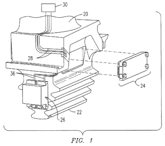
FIG. 1 is a partial isometric view of an exemplary turbine blade including
electronic circuitry, which may be used by a wireless telemetry system to
monitor
operational parameters of the blade.
FIG. 2 is a block diagram of an example strain gauge circuitry, which may be
used by the telemetry system, and which may benefit from a high-gain
differential
amplifier embodying aspects of the present invention.
FIG. 3 is a schematic representation of one example embodiment of an AC-
coupled hybrid-load differential amplifier embodying aspects of the present
invention.

CA 02877667 2014-12-19
WO 2014/004004 PCT/US2013/044268
2
FIG. 4 is a schematic representation of a single-stage differential amplifier
embodying aspects of the present invention, as may be integrated in one
example
strain gauge circuitry.
DETAILED DESCRIPTION OF THE INVENTION
Example embodiments of the present invention may be directed to electronic
circuitry, which, in one example application, may be used in an internal
combustion
engine, such as a turbine engine, instrumented with a telemetry system. This
example
application may allow transmitting sensor data from a movable component, such
as a
rotatable turbine engine blade, having certain electronic circuitry, which,
for example,
may operate in an environment having a temperature exceeding approximately 300
C.
For purposes of the disclosure herein, the term "high temperature" environment

without additional qualification may refer to any operating environment, such
as that
within portions of a turbine engine, having a maximum operating temperature
exceeding
approximately 300 'C. It will be appreciated that aspects of the present
invention are
not necessarily limited to a high temperature environment, since circuitry
embodying
aspects of the present invention may be used equally effective in a non-high
temperature environment.
FIG. 1 illustrates a turbine blade 20 (fragmentarily illustrated), as may be
instrumented with an example telemetry system, which may include a wireless
telemetry transmitter assembly 24 and an antenna assembly 26. Lead lines or
connectors 28 may extend from one or more sensors, such as sensor 30, to
telemetry
transmitter assembly 24, which may be mounted proximate a blade root 22 and
may
include various telemetry transmitter circuitry. Lead lines 28 may route
electronic data
signals from sensor 30 to telemetry transmitter assembly 24, where the signals
may be
processed by a processor. Further lead lines or electrical connectors 36 may
be used
for routing electronic data signals from telemetry transmitter circuitry to
antenna
assembly 26.
FIG. 2 illustrates a block diagram of an example strain gauge circuitry, which

may be used in a turbine component (e.g., turbine blade 20 (FIG. 1))
instrumented with
a telemetry system. A signal indicative of the amount of strain, which may
develop on a
measured turbine component, may be sensed by a strain gauge 101, which signal
may
be coupled to a differential amplifier 102. The output of the differential
amplifier 102

CA 02877667 2014-12-19
WO 2014/004004 PCT/US2013/044268
3
may be coupled to a voltage-controlled oscillator (VC0) 104, which may
generate an
oscillatory signal having a frequency, which is indicative of the amount of
strain which
develops on the measured turbine component. This oscillatory signal may be
buffered
by a buffer 105 and coupled to antenna 26 for transmission to an external
receiver (not
shown), which may be tuned to the carrier frequency.
FIGs. 3-4 and related description below will provide details of circuitry
embodying
aspects of the present invention, which in one example application, may be
used in
strain gauge circuitry, as exemplarily illustrated in FIG. 2. It will be
appreciated that such
example application should not be construed in a limiting sense being that
circuitry
embodying aspects of the present invention may be used in other applications.
FIG. 3 is a schematic representation of one example embodiment of circuitry
120
(also shown in FIG. 4) embodying aspects of the present invention. Circuitry
120
includes a differential amplifier 122 having an input terminal 124, which may
be coupled
to a sensing element (e.g., strain gauge 101 FIG. 2) to receive the voltage
indicative of
a sensed parameter (e.g., voltage indicative of strain). Differential
amplifier 122 may
include a first pair of semiconductor switches 126, 128 (e.g., differential
pair of
semiconductor switches). Biasing of the differential pair of semiconductor
switches 126,
128 may be controlled by a bridge circuit made up by resistors R5, R6, R7 and
R8 using
biasing techniques well-understood by one skilled in the art. Circuitry 120
further
includes a hybrid load circuitry 125, which in accordance with example aspects
of the
present invention may be AC-coupled (alternating current-coupled) to
differential
amplifier 122, as elaborated in greater detail below.
Hybrid load circuitry 125 may include a second pair of semiconductor switches
130,132 (e.g., active-load pair of semiconductor switches). Each of such pairs
of
semiconductor switches has a respective drain terminal (D), a respective
source
terminal (S) and a respective gating terminal (G). In one example embodiment,
the first
pair of semiconductor switches 126, 128 and the second pair of semiconductor
switches
130, 132 involve circuitry without complementary pairs of semiconductor
switches. In
one example embodiment, the first pair of semiconductor switches 126, 128 and
the
second pair of semiconductor switches 130,132 may be n-channel junction gate
field-
effect transistor (JFET) switches and may comprise a respective high-
temperature, wide

CA 02877667 2014-12-19
WO 2014/004004 PCT/US2013/044268
4
bandgap material, such as SiC, AN, GaN, AlGaN, GaAs, GaP, InP, Al GaAs, AlGaP,

AlinGaP, and GaAsAIN.
As will be appreciated by one skilled in the art, p-channel SiC JFETs are
presently believed to be impractical due to their relatively low-channel
mobility, and
consequently, known active load topologies for differential amplifiers have
not been
utilized in high-temperature applications since such topologies would involve
p-channel
SiC JFETs. Hybrid load circuitry embodying aspects of the present invention,
advantageously eliminates a need of p-channel JFETs, and thus such a circuitry
can
reach the theoretical temperature limits of high-temperature, wide bandgap
material
JFETs (e.g,, above 500 00) and effectively provide a high-gain differential
amplifier,
which, in one example application, may be utilized to appropriately amplify in
a high-
temperature environment the relatively low-voltage (e.g., a few millivolts)
electrical
signals, which may be generated by sensors, such as thermocouples and strain
gauges.
In one example embodiment, hybrid bad circuitry 125 may further comprise a
resistor-capacitor circuit 134 (e.g., a resistor 142 and a capacitor 140)
arranged to
provide a path (e.g., relatively high-impedance path) to an AC signal
component with
respect to the drain terminal of the switch of the differential pair of
semiconductor
switches, which receives the voltage indicative of the sensed parameter (e.g.,
switch
126). Circuit 134 is connected to a node 136 coupled in parallel circuit to
the respective
gate terminals of the second pair of semiconductor switches 130,132. It will
be
appreciated that node 136, which is connected to an electrical ground 135 by
way of
resistor 142 is effective to maintain an appropriate biasing for semiconductor
switches
130, 132.
In one example embodiment, the value of resistor 142 may be chosen to be
sufficiently low relative to the value of the input impedance at the
respective gate
terminals of switches 130, 132 so that, for example, an AC signal component at
the
drain terminal of differential switch 126, would be AC-coupled by way of
capacitor 140
to the path provided by resistor 142, in lieu of the gate terminals of
switches 130, 132.
For example, presuming an input impedance in the order of 20 MO at the
respective
gate terminal of switch pair 130,132 relative to a resistance value in the
order of 2 MO
for resistor 142, it would be appreciated that resistor-capacitor circuit 124
would effect a

CA 02877667 2014-12-19
WO 2014/004004 PCT/US2013/044268
high-impedance path to such AC signal component (e.g., at the drain of
differential
switch 126), and this effectively increases the AC gain of the differential
amplifier.
For biasing purposes, hybrid load circuitry 125 may include a first resistor
144
coupled from a source terminal of one of the switches of the second pair of
semiconductor switches (e.g., switch 130) to a drain terminal of one of the
switches of
the first pair of semiconductor switches (e.g., differential switch 126).
Hybrid load
circuitry 125 may further include a second resistor 146 coupled from a source
terminal
of the other one of the switches (e.g., switch 132) of the second pair of
semiconductor
switches to a drain terminal of the other one of the switches of the first
pair of
semiconductor switches (e.g, differential switch 128). A node 148 connected to
the
source terminal of switch 132 provides the amplified differential amplifier
output.
Preliminary experimental results have demonstrated feasibility of differential
gains of at
least approximately 47.8 dB, 51.4 dB and 57.8 dB at temperatures of 450 C,
300 C
and 25 'C, respectively.
FIG. 4 is a schematic representation of hybrid load single-stage differential
amplifier embodying aspects of the present invention, as may be integrated in
a
wireless telemetry system. Circuitry 120 may be arranged to amplify the AC
output
signal from a low-level output sensor (e.g., a strain gauge) and the amplified
output
signal from circuitry 120 may be signal-conditioned through a high-pass filter
160 and
passed to a voltage-controlled oscillator 162, which may be configured to
modulate a
radio-frequency (RF) carrier, It will be appreciated that the relatively high-
gain, which
can be obtained with a differential amplifier embodying aspects of the present
invention
can advantageously avoid a need of multiple stages of amplification (AC
amplifiers),
thereby incrementally reducing costs as well as providing substantial signal
integrity
(e.g., improved signal-to-noise ratio) and increasing system reliability
(e.g., less
interconnections).
While various embodiments of the present invention have been shown and
described herein, it will be apparent that such embodiments are provided by
way of
example only. Numerous variations, changes and substitutions may be made
without
departing from the invention herein. Accordingly, it is intended that the
invention be
limited only by the spirit and scope of the appended claims.

Representative Drawing
A single figure which represents the drawing illustrating the invention.
Administrative Status

For a clearer understanding of the status of the application/patent presented on this page, the site Disclaimer , as well as the definitions for Patent , Administrative Status , Maintenance Fee  and Payment History  should be consulted.

Administrative Status

Title Date
Forecasted Issue Date Unavailable
(86) PCT Filing Date 2013-06-05
(87) PCT Publication Date 2014-01-03
(85) National Entry 2014-12-19
Examination Requested 2014-12-19
Dead Application 2017-06-06

Abandonment History

Abandonment Date Reason Reinstatement Date
2016-06-06 FAILURE TO PAY APPLICATION MAINTENANCE FEE
2016-06-10 FAILURE TO PAY FINAL FEE

Payment History

Fee Type Anniversary Year Due Date Amount Paid Paid Date
Request for Examination $800.00 2014-12-19
Registration of a document - section 124 $100.00 2014-12-19
Application Fee $400.00 2014-12-19
Maintenance Fee - Application - New Act 2 2015-06-05 $100.00 2015-05-05
Owners on Record

Note: Records showing the ownership history in alphabetical order.

Current Owners on Record
SIEMENS ENERGY, INC.
ARKANSAS POWER ELECTRONICS INTERNATIONAL, INC.
Past Owners on Record
None
Past Owners that do not appear in the "Owners on Record" listing will appear in other documentation within the application.
Documents

To view selected files, please enter reCAPTCHA code :


To view images, click a link in the Document Description column. To download the documents, select one or more checkboxes in the first column and then click the "Download Selected in PDF format (Zip Archive)" or the "Download Selected as Single PDF" button.

List of published and non-published patent-specific documents on the CPD .

If you have any difficulty accessing content, you can call the Client Service Centre at 1-866-997-1936 or send them an e-mail at CIPO Client Service Centre.


Document
Description 
Date
(yyyy-mm-dd) 
Number of pages   Size of Image (KB) 
Abstract 2014-12-19 1 66
Claims 2014-12-19 4 246
Drawings 2014-12-19 3 63
Description 2014-12-19 5 475
Representative Drawing 2015-01-20 1 13
Cover Page 2015-02-20 1 48
PCT 2014-12-19 3 102
Assignment 2014-12-19 9 543
Correspondence 2015-03-05 6 291
Correspondence 2015-06-16 10 291