Note: Descriptions are shown in the official language in which they were submitted.
CA 02878252 2014-12-31
- 1 -
SP353163
DESCRIPTION
Title of Invention: DATA PROCESSING APPARATUS AND DATA
PROCESSING METHOD
Technical Field
[0001]
The present technology relates to a data processing
apparatus and a data processing method, and in particular,
relates to a data processing apparatus and a data processing
method which are able to secure good communication quality
in data transmission using, for example, an LDPC code.
Background Art
[0002]
A low density parity check (LDPC) code has a high error
correction ability, and has been widely adopted in a
transmission scheme including digital broadcasting such as,
for example, European digital video broadcasting (DVB)-S.2,
DVB-T.2, and DVB-C.2 in recent years (for example, see NPL
1).
[0003]
Recent studies show that the LDPC code has a
performance close to the Shannon limit, similar to turbo
codes or the like, with an increase in a code length. In
addition, since the LDPC code has properties of a minimum
distance being proportional to the code length, the LDPC
CA 02878252 2014-12-31
- 2 -
SP353163
code has an advantage in which a block error probability
characteristic is good and a so-called error floor
phenomenon observed as a decoding property of the turbo code
or the like hardly occurs, as properties.
Citation List
Non Patent Literature
[0004]
NPL 1: DVB-S.2: ETSI EN 302 307 V1.2.1 (2009-08)
Summary of Invention
Technical Problem
[0005]
In data transmission using an LDPC code, for example,
the LDPC code is formed into a symbol of quadrature
modulation (digital modulation) such as quadrature phase
shift keying (QPSK) (is symbolized), and the symbol is
transmitted by being mapped to the signal point of
quadrature modulation.
[0006]
Such data transmission using the LDPC code becomes
widespread worldwide, and securing good communication
quality has been requested.
[0007]
The present technology has been made in view of such
circumstances, and an object is to secure good communication
quality in data transmission using an LDPC code.
CA 02878252 2014-12-31
- 3 -
SP353163
Solution to Problem
[0008]
A first data processing apparatus/a data processing
method of the present technology includes a coding unit/step
that encodes an information bit into an LDPC code having a
code length of 16200 bits and a code rate of 12/15, based on
a parity check matrix of a low density parity check (LDPC)
code, in which the LDPC code includes an information bit and
a parity bit, the parity check matrix includes an
information matrix portion corresponding to the information
bit and a parity matrix portion corresponding to the parity
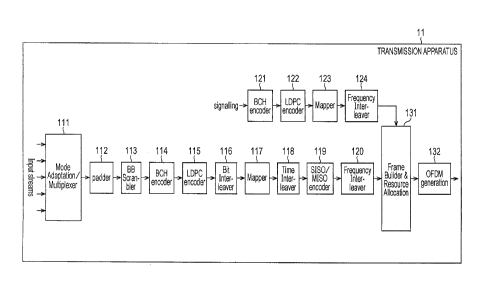
bit, the information matrix portion is represented by a
parity check matrix initial value table, the parity check
matrix initial value table is a table representing positions
of elements of 1 in the information matrix portion at an
interval of 360 columns, and is
3 394 1014 1214 1361 1477 1534 1660 1856 2745 2987 2991
3124 3155
59 136 528 781 803 928 1293 1489 1944 2041 2200 2613
2690 2847
155 245 311 621 1114 1269 1281 1783 1995 2047 2672 2803
2885 3014
79 870 974 1326 1449 1531 2077 2317 2467 2627 2811 3083
3101 3132
4 582 660 902 1048 1482 1697 1744 1928 2628 2699 2728
CA 02878252 2014-12-31
- 4 -
SP353163
3045 3104
175 395 429 1027 1061 1068 1154 1168 1175 2147 2359
2376 2613 2682
1388 2241 3118 3148
143 506 2067 3148
1594 2217 2705
398 988 2551
1149 2588 2654
678 2844 3115
1508 1547 1954
1199 1267 1710
2589 3163 3207
1 2583 2974
2766 2897 3166
929 1823 2742
1113 3007 3239
1753 2478 3127
0 509 1811
1672 2646 2984
965 1462 3230
3 1077 2917
1183 1316 1662
968 1593 3239
64 1996 2226
1442 2058 3181
CA 02878252 2014-12-31
- 5 -
SP353163
513 973 1058
1263 3185 3229
681 1394 3017
419 2853 3217
3 2404 3175
2417 2792 2854
1879 2940 3235
647 1704 3060.
[0009]
In the first data processing apparatus/data processing
method, an information bit is encoded into an LDPC code
having a code length of 16200 bits and a code rate of 12/15,
based on a parity check matrix of a low density parity check
(LDPC) code. The LDPC code includes an information bit and
a parity bit, the parity check matrix includes an
information matrix portion corresponding to the information
bit and a parity matrix portion corresponding to the parity
bit, the information matrix portion is represented by a
parity check matrix initial value table, the parity check
matrix initial value table is a table representing positions
of elements of 1 in the information matrix portion at an
interval of 360 columns, and is
3 394 1014 1214 1361 1477 1534 1660 1856 2745 2987 2991
3124 3155
59 136 528 781 803 928 1293 1489 1944 2041 2200 2613
CA 02878252 2014-12-31
- 6 -
SP353163
2690 2847
155 245 311 621 1114 1269 1281 1783 1995 2047 2672 2803
2885 3014
79 870 974 1326 1449 1531 2077 2317 2467 2627 2811 3083
3101 3132
4 582 660 902 1048 1482 1697 1744 1928 2628 2699 2728
3045 3104
175 395 429 1027 1061 1068 1154 1168 1175 2147 2359
2376 2613 2682
1388 2241 3118 3148
143 506 2067 3148
1594 2217 2705
398 988 2551
1149 2588 2654
678 2844 3115
1508 1547 1954
1199 1267 1710
2589 3163 3207
1 2583 2974
2766 2897 3166
929 1823 2742
1113 3007 3239
1753 2478 3127
0 509 1811
1672 2646 2984
CA 02878252 2014-12-31
- 7 -
SP353163
965 1462 3230
3 1077 2917
1183 1316 1662
968 1593 3239
64 1996 2226
1442 2058 3181
513 973 1058
1263 3185 3229
681 1394 3017
419 2853 3217
3 2404 3175
2417 2792 2854
1879 2940 3235
647 1704 3060.
[0010]
A second data processing apparatus/data processing
method of the present technology includes a decoding
unit/step that decodes an LDPC code which is obtained from
data transmitted from a transmission apparatus including a
coding unit that encodes an information bit into an LDPC
code having a code length of 16200 bits and a code rate of
12/15, based on a parity check matrix of a low density
parity check (LDPC) code, in which the LDPC code includes an
information bit and a parity bit, the parity check matrix
includes an information matrix portion corresponding to the
CA 02878252 2014-12-31
- 8 -
SP353163
information bit and a parity matrix portion corresponding to
the parity bit, the information matrix portion is
represented by a parity check matrix initial value table,
the parity check matrix initial value table is a table
representing positions of elements of 1 in the information
matrix portion at an interval of 360 columns, and is
3 394 1014 1214 1361 1477 1534 1660 1856 2745 2987 2991
3124 3155
59 136 528 781 803 928 1293 1489 1944 2041 2200 2613
2690 2847
155 245 311 621 1114 1269 1281 1783 1995 2047 2672 2803
2885 3014
79 870 974 1326 1449 1531 2077 2317 2467 2627 2811 3083
3101 3132
4 582 660 902 1048 1482 1697 1744 1928 2628 2699 2728
3045 3104
175 395 429 1027 1061 1068 1154 1168 1175 2147 2359
2376 2613 2682
1388 2241 3118 3148
143 506 2067 3148
1594 2217 2705
398 988 2551
1149 2588 2654
678 2844 3115
1508 1547 1954
CA 02878252 2014-12-31
- 9 -
SP353163
1199 1267 1710
2589 3163 3207
1 2583 2974
2766 2897 3166
929 1823 2742
1113 3007 3239
1753 2478 3127
0 509 1811
1672 2646 2984
965 1462 3230
3 1077 2917
1183 1316 1662
968 1593 3239
64 1996 2226
1442 2058 3181
513 973 1058
1263 3185 3229
681 1394 3017
419 2853 3217
3 2404 3175
2417 2792 2854
1879 2940 3235
647 1704 3060.
[0011]
In the second data processing apparatus/data processing
CA 02878252 2014-12-31
- 10 -
SP353163
method, an LDPC code which is obtained from data transmitted
from a transmission apparatus is decoded, in which the
transmission apparatus includes a coding unit/step that
encodes an information bit into an LDPC code having a code
length of 16200 bits and a code rate of 12/15, based on a
parity check matrix of a low density parity check (LDPC)
code, in which the LDPC code includes an information bit and
a parity bit, the parity check matrix includes an
information matrix portion corresponding to the information
bit and a parity matrix portion corresponding to the parity
bit, the information matrix portion is represented by a
parity check matrix initial value table, the parity check
matrix initial value table is a table representing positions
of elements of 1 in the information matrix portion at an
interval of 360 columns, and is
3 394 1014 1214 1361 1477 1534 1660 1856 2745 2987 2991
3124 3155
59 136 528 781 803 928 1293 1489 1944 2041 2200 2613
2690 2847
155 245 311 621 1114 1269 1281 1783 1995 2047 2672 2803
2885 3014
79 870 974 1326 1449 1531 2077 2317 2467 2627 2811 3083
3101 3132
4 582 660 902 1048 1482 1697 1744 1928 2628 2699 2728
3045 3104
CA 02878252 2014-12-31
11 -
SP353163
175 395 429 1027 1061 1068 1154 1168 1175 2147 2359
2376 2613 2682
1388 2241 3118 3148
143 506 2067 3148
1594 2217 2705
398 988 2551
1149 2588 2654
678 2844 3115
1508 1547 1954
1199 1267 1710
2589 3163 3207
1 2583 2974
2766 2897 3166
929 1823 2742
1113 3007 3239
1753 2478 3127
0 509 1811
1672 2646 2984
965 1462 3230
3 1077 2917
1183 1316 1662
968 1593 3239
64 1996 2226
1442 2058 3181
513 973 1058
CA 02878252 2014-12-31
- 12 -
SP353163
1263 3185 3229
681 1394 3017
419 2853 3217
3 2404 3175
2417 2792 2854
1879 2940 3235
647 1704 3060.
[0012]
A third data processing apparatus of the present
technology includes a decoding unit that decodes an LDPC
code having a code length of 16200 bits and a code rate of
12/15, based on a parity check matrix of a low density
parity check (LDPC) code, in which the LDPC code includes an
information bit and a parity bit, the parity check matrix
includes an information matrix portion corresponding to the
information bit and a parity matrix portion corresponding to
the parity bit, the information matrix portion is
represented by a parity check matrix initial value table,
,
the parity check matrix initial value table is a table
representing positions of elements of 1 in the information
matrix portion at an interval of 360 columns, and is
3 394 1014 1214 1361 1477 1534 1660 1856 2745 2987 2991
3124 3155
59 136 528 781 803 928 1293 1489 1944 2041 2200 2613
2690 2847
CA 02878252 2014-12-31
- 13 -
SP353163
155 245 311 621 1114 1269 1281 1783 1995 2047 2672 2803
2885 3014
79 870 974 1326 1449 1531 2077 2317 2467 2627 2811 3083
3101 3132
4 582 660 902 1048 1482 1697 1744 1928 2628 2699 2728
3045 3104
175 395 429 1027 1061 1068 1154 1168 1175 2147 2359
2376 2613 2682
1388 2241 3118 3148
143 506 2067 3148
1594 2217 2705
398 988 2551
1149 2588 2654
678 2844 3115
1508 1547 1954
1199 1267 1710
2589 3163 3207
1 2583 2974
2766 2897 3166
929 1823 2742
1113 3007 3239
1753 2478 3127
0 509 1811
1672 2646 2984
965 1462 3230
CA 02878252 2014-12-31
- 14 -
SP353163
3 1077 2917
1183 1316 1662
968 1593 3239
64 1996 2226
1442 2058 3181
513 973 1058
1263 3185 3229
681 1394 3017
419 2853 3217
3 2404 3175
2417 2792 2854
1879 2940 3235
647 1704 3060.
[0013]
In the third data processing apparatus, an LDPC code
having a code length of 16200 bits and a code rate of 12/15
is decoded, based on a parity check matrix of a low density
parity check (LDPC) code. The LDPC code includes an
information bit and a parity bit, the parity check matrix
includes an information matrix portion corresponding to the
information bit and a parity matrix portion corresponding to
the parity bit, the information matrix portion is
represented by a parity check matrix initial value table,
the parity check matrix initial value table is a table
representing positions of elements of 1 in the information
CA 02878252 2014-12-31
- 15 -
SP353163
matrix portion at an interval of 360 columns, and is
3 394 1014 1214 1361 1477 1534 1660 1856 2745 2987 2991
3124 3155
59 136 528 781 803 928 1293 1489 1944 2041 2200 2613
2690 2847
155 245 311 621 1114 1269 1281 1783 1995 2047 2672 2803
2885 3014
79 870 974 1326 1449 1531 2077 2317 2467 2627 2811 3083
3101 3132
4 582 660 902 1048 1482 1697 1744 1928 2628 2699 2728
3045 3104
175 395 429 1027 1061 1068 1154 1168 1175 2147 2359
2376 2613 2682
1388 2241 3118 3148
143 506 2067 3148
1594 2217 2705
398 988 2551
1149 2588 2654
678 2844 3115
1508 1547 1954
1199 1267 1710
2589 3163 3207
1 2583 2974
2766 2897 3166
929 1823 2742
CA 02878252 2014-12-31
- 16 -
SP353163
1113 3007 3239
1753 2478 3127
0 509 1811
1672 2646 2984
965 1462 3230
3 1077 2917
1183 1316 1662
968 1593 3239
64 1996 2226
1442 2058 3181
513 973 1058
1263 3185 3229
681 1394 3017
419 2853 3217
3 2404 3175
2417 2792 2854
1879 2940 3235
647 1704 3060.
[0014]
In addition, the data processing apparatus may be an
independent apparatus or may be an internal block
configuring one apparatus.
Advantageous Effects of Invention
[0015]
According to the present invention, it is possible to
CA 02878252 2014-12-31
- 17 -
SP353163
secure good communication quality in data transmission using
an LDPC code.
[0016]
In addition, the effects described herein are merely
illustrative, the effects of the present technology are not
intended to be limited to the effects which are described
herein, and there may be additional effects.
Brief Description of Drawings
[0017]
[Fig. 1] Fig. 1 is a diagram describing a parity check
matrix H of an LDPC code.
[Fig. 2] Fig. 2 is a flowchart illustrating a decoding
procedure of the LDPC code.
[Fig. 3] Fig. 3 is a diagram illustrating an example of
a parity check matrix of the LDPC code.
[Fig. 4] Fig. 4 is a diagram illustrating a Tanner
graph of the parity check matrix.
[Fig. 5] Fig. 5 is a diagram illustrating a variable
node.
[Fig. 6] Fig. 6 is a diagram illustrating a check node.
[Fig. 7] Fig. 7 is a diagram illustrating a
configuration example of an embodiment of a transmission
system to which the present technology is applied.
[Fig. 8] Fig. 8 is a diagram illustrating a
configuration example of a transmission apparatus 11.
CA 02878252 2014-12-31
- 18 -
SP353163
[Fig. 9] Fig. 9 is a block diagram illustrating a
configuration example of a bit interleaver 116.
[Fig. 10] Fig. 10 is a diagram illustrating a parity
check matrix.
[Fig. 11] Fig. 11 is a diagram illustrating a parity
matrix.
[Fig. 12] Fig. 12 is a diagram illustrating a parity
check matrix of the LDPC code which is defined in the DVB-
S.2 standard.
[Fig. 13] Fig. 13 is a diagram describing the parity
check matrix of the LDPC code which is defined in the DVB-
S.2 standard.
[Fig. 14] Fig. 14 is a diagram illustrating a signal
point arrangement of 16QAM.
[Fig. 15] Fig. 15 is a diagram illustrating a signal
point arrangement of 64QAM.
[Fig. 16] Fig. 16 is a diagram illustrating a signal
point arrangement of 64QAM.
[Fig. 17] Fig. 17 is a diagram illustrating a signal
point arrangement of 64QAM.
[Fig. 18] Fig. 18 is a diagram illustrating a signal
point arrangement which is defined in the DVB-S.2 standard.
[Fig. 19] Fig. 19 is a diagram illustrating a signal
point arrangement which is defined in the DVB-S.2 standard.
[Fig. 20] Fig. 20 is a diagram illustrating a signal
CA 02878252 2014-12-31
- 19 -
SP353163
point arrangement which is defined in the DVB-S.2 standard.
[Fig. 21] Fig. 21 is a diagram illustrating a signal
point arrangement which is defined in the DVB-S.2 standard.
[Fig. 22] Fig. 22 is a diagram describing a process of
a demultiplexer 25.
[Fig. 23] Fig. 23 is a diagram describing a process of
the demultiplexer 25.
[Fig. 24] Fig. 24 is a diagram illustrating a Tanner
graph for decoding of the LDPC code.
[Fig. 25] Fig. 25 is a diagram illustrating a parity
matrix HT having a staircase structure and a Tanner graph
corresponding to the parity matrix HT.
[Fig. 26] Fig. 26 is a diagram illustrating a parity
matrix HT of a parity check matrix H corresponding to an
LDPC code after parity interleave.
[Fig. 27] Fig. 27 is a diagram illustrating a
conversion parity check matrix.
[Fig. 28] Fig. 28 is a diagram describing a process of
a column twist interleaver 24.
[Fig. 29] Fig. 29 is a diagram illustrating the number
of columns and an address of a write start position of a
memory 31 required for column twist interleave.
[Fig. 30] Fig. 30 is a diagram illustrating the number
of columns and an address of a write start position of the
memory 31 required for column twist interleave.
CA 02878252 2014-12-31
- 20 -
SP353163
[Fig. 31] Fig. 31 is a flowchart illustrating a process
performed in a bit interleaver 116 and a mapper 117.
[Fig. 32] Fig. 32 is a diagram illustrating a
communication path model employed in a simulation.
[Fig. 33] Fig. 33 is a diagram illustrating a
relationship between an error rate obtained by the
simulation and a Doppler frequency fd of a flutter.
[Fig. 34] Fig. 34 is a diagram illustrating a
relationship between an error rate obtained by the
simulation and a Doppler frequency fd of a flutter.
[Fig. 35] Fig. 35 is a block diagram illustrating a
configuration example of an LDPC encoder 115.
[Fig. 36] Fig. 36 is a flowchart illustrating a process
of the LDPC encoder 115.
[Fig. 37] Fig. 37 is a diagram illustrating an example
of a parity check matrix initial value table in which a code
rate is 1/4 and a code length is 16200.
[Fig. 38] Fig. 38 is a diagram describing a method of
obtaining a parity check matrix H from the parity check
matrix initial value table.
[Fig. 39] Fig. 39 is a diagram illustrating an example
of a parity check matrix initial value table of a 16k code
with r=12/15.
[Fig. 40] Fig. 40 is a diagram illustrating an example
of a Tanner graph of ensemble of a degree sequence in which
CA 02878252 2014-12-31
- 21 -
SP353163
a column weight is 3 and a row weight is 6.
[Fig. 41] Fig. 41 is a diagram illustrating an example
of a Tanner graph of a multi-edge type ensemble.
[Fig. 42] Fig. 42 is a diagram illustrating a minimum
cycle length and a performance threshold of a parity check
matrix of 16k code with r=12/15.
[Fig. 43] Fig. 43 is a diagram describing a parity
check matrix of 16k code with r=12/15.
[Fig. 44] Fig. 44 is a diagram describing a parity
check matrix of 16k code with r=12/15.
[Fig. 45] Fig. 45 is a diagram illustrating a
simulation result of simulation of measuring BER/FER.
[Fig. 46] Fig. 46 is a block diagram illustrating a
configuration example of a reception apparatus 12.
[Fig. 47] Fig. 47 is a block diagram illustrating a
configuration example of a bit deinterleaver 165.
[Fig. 48] Fig. 48 is a flowchart illustrating a process
performed by a demapper 164, the bit deinterleaver 165, and
an LDPC decoder 166.
[Fig. 49] Fig. 49 is a diagram illustrating an example
of a parity check matrix of an LDPC code.
[Fig. 50] Fig. 50 is a diagram illustrating a matrix
(conversion parity check matrix) obtained by performing row
permutation and column permutation on a parity check matrix.
[Fig. 51] Fig. 51 is a diagram illustrating a
CA 02878252 2014-12-31
- 22 -
SP353163
conversion parity check matrix which is divided into 5x5
units.
[Fig. 52] Fig. 52 is a block diagram illustrating a
configuration example of a decoding device that performs
node calculation in groups of P.
[Fig. 53] Fig. 53 is a block diagram illustrating a
configuration example of the LDPC decoder 166.
[Fig. 54] Fig. 54 is a diagram describing a process of
a multiplexer 54 configuring the bit deinterleaver 165.
[Fig. 55] Fig. 55 is a diagram describing a process of
a column twist deinterleaver 55.
[Fig. 56] Fig. 56 is a block diagram illustrating
another configuration example of the bit deinterleaver 165.
[Fig. 57] Fig. 57 is a block diagram illustrating a
first configuration example of a reception system to which
the reception apparatus 12 is applicable.
[Fig. 58] Fig. 58 is a block diagram illustrating a
second configuration example of a reception system to which
the reception apparatus 12 is applicable.
[Fig. 59] Fig. 59 is a block diagram illustrating a
third configuration example of a reception system to which
the reception apparatus 12 is applicable.
[Fig. 60] Fig. 60 is a block diagram illustrating a
configuration example of an embodiment of a computer to
which the present technology is applied.
CA 02878252 2014-12-31
- 23 -
SP353163
Description of Embodiments
[0018]
Hereinafter, an LDPC code will be described before a
description of embodiments of the present technology.
[0019]
<LDPC code>
[0020]
Further, the LDPC code is a linear code, and does not
need to be binary, but here, a description will be given
assuming that the LDPC code is binary.
[0021]
The most significant feature of the LDPC code is that a
parity check matrix defining the LDPC code is a sparse
matrix. Here, the sparse matrix is a matrix in which the
number of "1" elements of the matrix is very small (most
elements in the matrix are 0).
[0022]
Fig. 1 is a diagram illustrating a parity check matrix
H of the LDPC code.
[0023]
In the parity check matrix H of Fig. 1, a weight of
each column (a column weight) (the number of "1") (a weight)
is set to "3", and a weight of each row (a row weight) is
set to "6".
CA 02878252 2014-12-31
- 24 -
SP353163
[0024]
In the coding using the LDPC code (LDPC coding), for
example, a generation matrix G is generated based on the
parity check matrix H, and a codeword (LDPC code) is
generated by multiplying the generation matrix G with a
binary information bit.
[0025]
Specifically, a coding device which performs LDPC
coding first calculates a generation matrix G in which an
equation GHT=0 is established between the parity check
matrix H and the transposed matrix HT thereof. Here, when
the generation matrixGisaKxNmatrix, the coding device
multiplies a bit sequence (vector u) of an information bit
formed of K bits with the generation matrix G so as to
generate a codeword c (=uG) formed of N bits. The codeword
(LDPC code) generated by the coding device is received on
the receiving side through a predetermined communication
path.
[0026]
The decoding of the LDPC code is an algorithm that is
proposed and referred to as probabilistic decoding by
Gallager, and the algorithm may be performed by a message
passing algorithm by belief propagation on a so-called
Tanner graph which is configured with a variable node (also
referred to as a message node) and a check node. Here,
CA 02878252 2014-12-31
- 25 -
SP353163
hereinafter, as appropriate, the variable node and the check
node are simply referred to as a node.
[0027]
Fig. 2 is a flowchart illustrating a decoding procedure
of the LDPC code.
[0028]
Further, hereinafter, as appropriate, a real number
(received LLR), which is obtained by representing the "0"
likelihood of a value of the i-th code bit of the LDPC code
(1 codeword) received on the receiving side as a log
likelihood ratio, is referred to as a received value uoi.
Further, the message output from the check node is assumed
to be uj, and the message output from the variable node is
assumed to be vi.
[0029]
First, in decoding of the LDPC code, as illustrated in
Fig. 2, in step S11, the LDPC code is received, the message
(check node message) uj is initialized to "0", a variable k
which is an integer as a counter of an iterative process is
initialized to "0", and the process proceeds to step S12.
In step S12, the message (variable node message) v, is
obtained by performing the calculation (variable node
calculation) shown in Equation (1) based on the received
value uo, obtained by receiving the LDPC code, and the
message uj is obtained by performing the calculation (check
CA 02878252 2014-12-31
- 26 -
SP353163
node calculation) shown in Equation (2), based on the
message vi.
[0030]
[Math. 1]
c18-1
Vi==Uoi+ Uj
j=1
[0031]
[Math. 2]
d ¨1
Vi
tanh = 11 tanh)
2 i=1
[0032]
Here, d, and d, in the equation (1) and the equation (2)
are respectively parameters indicating the number of "1" in
the vertical direction (column) and the horizontal direction
(row) of the parity check matrix H, which can be arbitrarily
selected. For example, in the case of the LDPC code shown
in Fig. 1 in which the column weight is 3 and the row weight
is 6 ((3, 6) LDPC code), it is established that dv=3 and d,=6.
[0033]
In addition, in the variable node calculation of the
equation (1) and the check node calculation of the equation
(2), a message which is input from an edge (a line
connecting the variable node and the check node) from which
CA 02878252 2014-12-31
- 27 -
SP353163
a message is to be output is not used as a target of
calculation, and thus a calculation range is 1 to d,-1 or 1
to d,-1. Further, the check node calculation of the equation
(2) is performed actually by previously creating a table of
a function R(vi, v2) shown in equation (3) which is defined
as one output for two inputs vl and v2 and continuously
(recursively) using the table as shown in equation (4).
[0034]
[Math. 3]
x=2tanh-1 ttanh (v1/2) tanh (v2/2) I =R (v1, v2)
¨(3)
[0035]
[Math. 4]
R (v2, R (v3, ...R (vdc_2, vdo_i ) )) )
[0036]
In step S12, the variable k is incremented by "1", and
the process proceeds to step S13. In step S13, it is
determined whether or not the variable k is greater than a
predetermined iterative decoding number C. In step S13, if
the variable k is determined not to be greater than C, the
process returns to step S12, and the same process is
repeated.
[0037]
Further, in step S13, if the variable k is determined
CA 02878252 2014-12-31
- 28 -
SP353163
to be greater than C, the process proceeds to step S14, a
message vl as a decoding result to be finally output is
obtained and output by performing the calculation shown in
the equation (5), and the decoding process of the LDPC code
is ended.
[0038]
[Math. 5]
d,
Vi"4=U01f Uj
[0039]
Here, the calculation of the equation (5) is different
from the variable node calculation of the equation (1), and
is performed by using the message uj from all edges coupled
to the variable node.
[0040]
Fig. 3 is a diagram illustrating an example of a parity
check matrix H of (3, 6) LDPC code (code rate of 1/2, code
length of 12).
[0041]
In the parity check matrix H of Fig. 3, a column weight
is set to 3 and a row weight is set to 6, similarly to Fig.
1.
[0042]
Fig. 4 is a diagram illustrating a Tanner graph of the
CA 02878252 2014-12-31
- 29 -
SP353163
parity check matrix H in Fig. 3.
[0043]
Here, in Fig. 4, check nodes are indicated by plus "+",
and variable nodes are indicated by equal "=". The check
nodes and the variable nodes respectively correspond to the
rows and the columns of the parity check matrix H. The
connection lines between the check nodes and the variable
nodes are edges, and the edges corresponds to "1" elements
in the parity check matrix.
[0044]
In other words, if the element in the j-th row and the
i-th column of the parity check matrix is 1, in Fig. 4, the
i-th variable node (node of "=") from the top and the j-th
and the check node (node of "+") from the top are coupled by
an edge. The edge represents that the code bit
corresponding to the variable node has constraints
corresponding to the check node.
[0045]
In a sum product algorithm which is a decoding method
of the LDPC code, the variable node calculation and the
check node calculation are repeatedly performed.
[0046]
Fig. 5 is a diagram illustrating a variable node
calculation performed at a variable node.
[0047]
CA 02878252 2014-12-31
- 30 -
SP353163
In the variable node, a message v, corresponding to an
edge to be calculated is obtained by the variable node
calculation of equation (1) using messages u1 and u2 from the
remaining edges which are connected to the variable node and
a received value un. The messages corresponding to other
edges are obtained in the same manner.
[0048]
Fig. 6 is a diagram illustrating a check node
calculation performed at the check node.
[0049]
Here, the check node calculation of the equation (2)
may be rewritten into an equation (6) by using a
relationship of an equation
axb=expfln(laj)+1n(Ibl) xsign ( a ) xsign (b ) . Here, sign (x ) is 1
when and sign(x) is -1 when x<0.
[0050]
[Math. 6]
Vi
U = =2tanh-1 TT tanh (-2)
i=1
c10-1 /dc-1
=2tanh-1 exp In tanh( }x"rj sign tanh( __
L
1=1 2 \ I 1=1 1 jj
( dc-1 / \NH dc-1
=2tanh-1 exp ¨ ¨In tanh2' x sign(vi)
1=1 / , 1=1
_
( 6 )
[0051]
CA 02878252 2014-12-31
- 31 -
SP353163
When xn, if a function T(x) is defined as an equation
cp(x)=Ln(tanh(x/2)), it is established that an equation T-
1 -1 -x
(x)=2tanh (e ), such that the equation (6) can be deformed
to the equation (7).
[0052]
[Math. 7]
(c10-1 dc-1
01-1== X. 45(IV1l) x TT s gn (v i)
i=1
-(7)
[0053]
In the check node, the check node calculation of the
equation (2) is performed according to the equation (7).
[0054]
In other words, in the check node, as illustrated in
Fig. 6, a message Uj corresponding to an edge to be
calculated is obtained by the check node calculation of the
equation (7) using messages vl, v2, v3, v4, and v5 from the
remaining edges which are connected to the check node. The
messages corresponding to other edges are obtained in the
same manner.
[0055]
In addition, a function y(x) of the equation (7) can be
represented as an equation y(x)=1n((ex+1)/(ex-1)), when x>0,
T(x)=T-1(x). When the functions y(x) and y-1(x) are
implemented in hardware, the functions may be implemented by
CA 02878252 2014-12-31
- 32 -
SP353163
using look up tables (LUTs) in some cases, but the LUTs are
the same.
[0056]
<Configuration example of transmission system to which
the present technology is applied>
[0057]
Fig. 7 is a diagram illustrating a configuration
example of an embodiment of a transmission system to which
the present technology is applied (the system refers to
those in which a plurality of devices are assembled
logically, and it does not matter whether the constituent
devices are in the same housing).
[0058]
In Fig. 7, the transmission system includes a
transmission apparatus 11 and a reception apparatus 12.
[0059]
The transmission apparatus 11 performs transmission
(broadcasting) (sending) of, for example, programs and the
like of television broadcasting. In other words, the
transmission apparatus 11 encodes, for example, target data
which is a target of transmission such as image data and
audio data as a program into an LDPC code, and transmits the
encoded target data through a communication path 13 such as,
for example, satellite lines, terrestrial waves, cables
(wired lines).
CA 02878252 2014-12-31
- 33 -
SP353163
[0060]
The reception apparatus 12 receives the LDPC code which
is transmitted from the transmission apparatus 11 through
the communication path 13, decodes the LDPC code into target
data, and outputs the data.
[0061]
Here, it has been known that the LDPC code used in the
transmission system of Fig. 7 exerts a significantly high
capacity in an Additive White Gaussian Noise (AWGN)
communication path.
[0062]
Meanwhile, the communication path 13 may generate a
burst error or erasure. For example, in particular, when
the communication path 13 is terrestrial waves, in an
Orthogonal Frequency Division Multiplexing (OFDM) system, in
a multipath environment in which a Desired to Undesired
Ratio (D/U) is 0 dB (power of Undesired=echo is equal to
power of Desired=main path), the power of a certain symbol
becomes 0 (erasure) according to the delay of echo (a path
other than the main path).
[0063]
Further, even in flutter (a communication path in which
delay is 0 and an echo due to a dopper frequency is added),
if the D/U is 0 dB, the power of all OFDM symbols at a
specific time may become 0 (erasure) due to the Doppler
CA 02878252 2014-12-31
- 34 -
SP353163
frequency.
[0064]
Further, a burst error may occur due to the status of
the wiring from a reception unit (not shown) such as an
antenna which receives signals from the transmission
apparatus 11 on the reception apparatus 12 to the reception
apparatus 12, and the instability of power of the reception
apparatus 12.
[0065]
Meanwhile, in the decoding of the LDPC code, in the
column of the parity check matrix H and the variable node
corresponding to the code bit of the LDPC code, as
illustrated in Fig. 5, since the variable node calculation
of the equation (1) with the addition of the code bit (the
received value un thereof) of the LDPC code is performed, if
an error occurs in the code bit used in the variable node
calculation, the accuracy of the obtained message is reduced.
[0066]
Then, in the decoding of the LDPC code, since the check
node calculation of the equation (7) in the check node is
performed by using the message that is obtained in the
variable node that is connected to the check node, if the
number of check nodes, in which a plurality of variable
nodes connected thereto (code bit of the LDPC code
corresponding thereto) simultaneously become error state
CA 02878252 2014-12-31
- 35 -
SP353163
(including erasure), is increased, the performance of
decoding is degraded.
[0067]
In other words, for example, if two or more of variable
nodes connected to the check node are simultaneously erased,
the check node returns a message in which a probability of
having a value 0 and a probability of having a value 1 are
the same in all variable nodes. In this case, the check
node that returns the message of the equal probability does
not contribute to one decoding process (one set of variable
node calculation and check node calculation), as a result, a
lot number of iterations of the decoding process is required,
the decoding performance is deteriorated, and the power
consumption of the reception apparatus 12 that decodes the
LDPC code increases.
[0068]
Thus, the transmission system of Fig. 7 enables
improvement in resistance to the burst error and erasure
while maintaining the performance at the AWGN communication
path (AWGN channel).
[0069]
<Configuration example of transmission apparatus 11>
[0070]
Fig. 8 is a block diagram illustrating a configuration
example of the transmission apparatus 11 in Fig. 7.
CA 02878252 2014-12-31
- 36 -
SP353163
[0071]
In the transmission apparatus 11, input streams of one
or more as target data are supplied to a mode
adaptation/multiplexer 111.
[0072]
The mode adaptation/multiplexer 111 performs a process
such as mode selection and multiplexing of one or more input
streams supplied thereto, as necessary, and supplies the
resulting data to a padder 112.
[0073]
The padder 112 performs necessary zero padding (null
insertion) on the data from the mode adaptation/multiplexer
111, and supplies the resulting data to a BB scrambler 113.
[0074]
The BB scrambler 113 performs Base-Band Scrambling (BB
scrambling) on the data from the padder 112, and supplies
the resulting data to a BCH encoder 114.
[0075]
The BCH encoder 114 performs BCH coding on the data
from the BB scrambler 113, and supplies the resulting data
as the LDPC target data which is the target of LDPC coding,
to an LDPC encoder 115.
[0076]
The LDPC encoder 115 performs LDPC coding according to
the parity check matrix in which the parity matrix which is
CA 02878252 2014-12-31
- 37 -
SP353163
a portion corresponding to parity bits of the LDPC code has
a staircase structure, on the LDPC target data from the BCH
encoder 114, and outputs the LDPC code with the LDPC target
data as an information bit.
[0077]
In other words, the LDPC encoder 115 performs LDPC
coding which encodes the LDPC target data into an LDPC code
(corresponding to the parity check matrix) which is defined
in predetermined standards such as, for example, DVB-S.2,
DVB-T.2, and DVB-C.2, or an LDPC code (corresponding to the
parity check matrix) which is determined in advance, and
outputs the resulting LDPC code.
[0078]
Here, the LDPC code which is defined in standards such
as DVB-S.2, DVB-T.2, and DVB-C.2 is an Irregular Repeat
accumulate (IRA) code, and the parity matrix in the parity
check matrix of the LDPC code has a staircase structure.
The parity matrix and the stair structure will be described
later. Further, the IRA code is described in, for example,
"Irregular Repeat-accumulate Codes," H. Jin, A. Khandekar,
and R.J. McEliece, in Proceedings of 2nd International
Symposium on Turbo codes and Related Topics, pp. 1-8, Sept.
2000.
[0079]
The LDPC code output from the LDPC encoder 115 is
CA 02878252 2014-12-31
- 38 -
SP353163
supplied to a bit interleaver 116.
[0080]
The bit interleaver 116 performs a bit interleave which
will be described later, on the LDPC code from the LDPC
encoder 115, and supplies the LDPC code after the bit
interleave to a mapper 117.
[0081]
The mapper 117 performs a quadrature modulation
(multilevel modulation) by mapping the LDPC code from the
bit interleaver 116 to a signal point representing one
symbol of the quadrature modulation, in a unit of code bit
of one bit or more of the LDPC code (symbol unit).
[0082]
In other words, the mapper 117 performs quadrature
modulation by mapping the LDPC code from the bit interleaver
116 to the signal points which are determined in a
modulation scheme which performs the quadrature modulation
of the LDPC code, on an IQ plane (IQ constellation) which is
defined as an I axis representing an I component which is
in-phase with a carrier wave and a Q axis representing a Q
component which is orthogonal to the carrier wave.
[0083]
Here, an example of a modulation scheme of the
quadrature modulation performed in the mapper 117 includes
for example, a modulation scheme which is defined in
CA 02878252 2014-12-31
- 39 -
SP353163
standards such as DVB-S.2, DVB-T.2, and DVB-C.2, the other
modulation schemes, in other words, for example, binary
phase shift keying (BPSK), quadrature phase shift keying
(QPSK), 8 phase shift keying (PSK), 16 amplitude phase-shift
keying (APSK), 32 APSK, 16 quadrature amplitude modulation
(QAM), 64QAM, 256QAM, 1024QAM, 4096QAM, and 4 pulse
amplitude modulation (PAM). In the mapper 117, a modulation
scheme by which quadrature modulation is performed is set in
advance, for example, according to an operator's operation
of the transmission apparatus 11.
[0084]
The data which is obtained by a process in the mapper
117 (a mapping result obtained by mapping a symbol into a
signal point) is supplied to a time interleaver 118.
[0085]
The time interleaver 118 performs time interleave
(interleave in a time direction) in a unit of symbol, on the
data from the mapper 117, and supplies the resulting data to
a Single Input Single Output/Multiple Input Single Output
(SISO/MISO) encoder 119.
[0086]
The SISO/MISO encoder 119 performs space-time coding on
the data from the time interleaver 118, and supplies the
resulting data to a frequency interleaver 120.
[0087]
CA 02878252 2014-12-31
- 40 -
SP353163
The frequency interleaver 120 performs frequency
interleave (interleave in a frequency direction) in a unit
of symbol, on the data from the SISO/MISO encoder 119, and
supplies the resulting data to a frame builder/resource
allocation unit 131.
[0088]
Meanwhile, for example, control data for transmission
control such as Base Band Signaling (BB signaling) (BB
Header) is supplied to a BCH encoder 121.
[0089]
The BCH encoder 121, similarly to the BCH encoder 114,
performs BCH coding on the control data supplied thereto,
and supplies the resulting data to an LDPC encoder 122.
[0090]
The LDPC encoder 122, similarly to the LDPC encoder 115,
performs LDPC coding on the data from the BCH encoder 121 as
the LDPC target data, and supplies the resulting LDPC code
to a mapper 123.
[0091]
The mapper 123, similarly to the mapper 117, performs a
quadrature modulation by mapping the LDPC code from the LDPC
encoder 122 to a signal point representing one symbol of the
quadrature modulation, in a unit of code bit of one bit or
more of the LDPC code (symbol unit), and supplies the
resulting data to a frequency interleaver 124.
CA 02878252 2014-12-31
- 41 -
SP353163
[0092]
The frequency interleaver 124, similarly to the
frequency interleaver 120, performs a frequency interleave
in a symbol unit on the data from the mapper 123, and
supplies the resulting data to the frame builder/resource
allocation unit 131.
[0093]
The frame builder/resource allocation unit 131 inserts
a pilot symbol in a necessary position of data (symbol) from
the frequency interleavers 120 and 124, makes a frame formed
of symbols of a predetermined number (for example, a
Physical Layer (PL) frame, a T2 frame, a 02 frame, and the
like) from the resulting data (symbol), and supplies the
frame to an OFDM generation unit 132.
[0094]
The OFDM generation unit 132 generates an OFDM signal
corresponding to the frame, from the frame from the frame
builder/resource allocation unit 131, and transmits the OFDM
signal through the communication path 13 (Fig. 7).
[0095]
In addition, the transmission apparatus 11 may be
configured without providing some of the blocks shown in Fig.
8 such as, for example, the time interleaver 118, the
SISO/MISO encoder 119, the frequency interleaver 120, and
the frequency interleaver 124.
CA 02878252 2014-12-31
- 42 -
SP353163
[0096]
Fig. 9 illustrates a configuration example of a bit
interleaver 116 in Fig. 8.
[0097]
The bit interleaver 116 has a function of interleaving
data, and is configured with a parity interleaver 23, a
column twist interleaver 24, and a demultiplexer (DEMUX) 25.
In addition, the bit interleaver 116 may be configured
without providing one or both of the parity interleaver 23
and the column twist interleaver 24.
[0098]
The parity interleaver 23 performs parity interleave
which interleaves the parity bit of the LDPC code from the
LDPC encoder 115 in the position of another parity bit, and
supplies the LDPC code after the parity interleave to the
column twist interleaver 24.
[0099]
The column twist interleaver 24 performs the column
twist interleave on the LDPC code from the parity
interleaver 23, and supplies the LDPC code after the column
twist interleave to the demultiplexer 25.
[0100]
In other words, the LDPC code is transmitted while the
code bits of one bit or more of the LDPC code are mapped to
a signal point representing one symbol of the quadrature
CA 02878252 2014-12-31
- 43 -
SP353163
modulation by the mapper 117 in Fig. 8.
[0101]
In the column twist interleaver 24, for example, a
column twist interleave, which will be described later, is
performed as a rearrangement process of rearranging the code
bits of the LDPC code from the parity interleaver 23 such
that a plurality of code bits of an LDPC code corresponding
to any 1 in any one row of the parity check matrix used in
the LDPC encoder 115 are not included in one symbol.
[0102]
The demultiplexer 25 obtains an LDPC code having
enhanced resistance to AWGN and the like by performing a
replacing process of replacing the position of two or more
code bits of the LDPC code which is a symbol, on the LDPC
code from the column twist interleaver 24. Then, the
demultiplexer 25 supplies the two or more code bits of the
LDPC code which is obtained by the replacing process, as a
symbol, to the mapper 117 (Fig. 8).
[0103]
Fig. 10 is a diagram illustrating the parity check
matrix H used in LDPC coding in the LDPC encoder 115 in Fig.
8.
[0104]
The parity check matrix H has a Low-Density Generation
Matrix (LDGM) structure, and can be represented by an
CA 02878252 2014-12-31
- 44 -
SP353163
equation H=[HAIHT] (a matrix in which the elements of an
information matrix HA are left elements and the elements of
a parity matrix HT are right elements) by the information
matrix HA of parts corresponding to the information bit and
the parity matrix HT of parts corresponding to the parity
bit, out of code bits of the LDPC code.
[0105]
Here, the number of bits of the information bit and the
number of bits of the parity bit out of code bits of one
LDPC code (1 codeword) are respectively referred to as an
information length K and a parity length M, and the number
of code bits of one LDPC code is referred to as a code
length N(=K+M).
[0106]
The information length K and the parity length M for
the LDPC code of a certain code length N are determined by a
code rate. Further, the parity check matrix H is a matrix
of row x column M x N. Then, the information matrix HA is a
matrix of M x K, and the parity matrix HT is a matrix of M x
M.
[0107]
Fig. 11 shows the parity matrix HT of the parity check
matrix H of the LDPC code which is defined in the standard
of DVB-S.2, DVB-T.2, and DVB-C.2.
[0108]
CA 02878252 2014-12-31
- 45 -
SP353163
As illustrated in Fig. 11, the parity matrix HT of the
parity check matrix H of the LDPC code which is defined in
the standard such as DVB-T.2 is a matrix of a staircase
structure in which elements of 1 are arranged in a staircase
shape (lower bidiagonal matrix). The row weight of the
parity matrix HT is 1 in a first row, and is 2 in all
remaining rows. Further, the column weight is 1 in a last
column, and is 2 in all remaining columns.
[0109]
As described above, it is possible to easily generate
the LDPC code of the parity check matrix H of which the
parity matrix HT has a staircase structure, by using the
parity check matrix H.
[0110]
In other words, the LDPC code (one codeword) is
represented by a row vector c, and a column vector obtained
by transporting the row vector is represented by cT. Further,
the information bit part is represented by a row vector c,
and the parity bit part is represented by a row vector T, in
the row vector c which is the LDPC code.
[0111]
In this case, the row vector c is represented by an
equation c =[AIT] (a row vector in which elements of the row
vector A are left elements and elements of the row vector T
are right elements) by using the row vector A as the
CA 02878252 2014-12-31
- 46 -
SP353163
information bit and the row vector T as the parity bit.
[0112]
It is necessary for the parity check matrix H and the
row vector c=[AIT] as the LDPC code to satisfy an equation
HcT=0, and if the parity matrix HT of the parity check matrix
H=[HAIHT] has the staircase structure shown in Fig. 11, the
row vector T as the parity bits configuring the row vector
c=[AT] satisfying the equation HcT=0 can be obtained
sequentially (in order) by making the element of each row 0
from the element of the first row of the column vector HcT
in order in the equation HcT=0.
[0113]
Fig. 12 is a diagram describing the parity check matrix
H of the LDPC code which is defined in the standard of DVB-
T.2.
[0114]
In the parity check matrix H of the LDPC code which is
defined in the standard of DVB-T.2, the column weight X is
given to the first column to a KX-th column, and the column
weight 3 is given to the subsequent K3 columns, the column
weight 2 is given to the subsequent M-1 columns, and the
column weight 1 is given to the last column.
[0115]
Here, KX+K3+M-1+1 is equal to the code length N.
[0116]
CA 02878252 2014-12-31
- 47 -
SP353163
Fig. 13 is a diagram illustrating the number of columns
KX, K3, and M, and a column weight X for each code rate of
the LDPC code which is defined in the standards of DVB-T.2
and the like.
[0117]
In the standards of DVB-T.2 and the like, the LDPC
codes of the code length N of 64800 bits and 16200 bits are
defined.
[0118]
Then, 11 code rates (nominal rates) 1/4, 1/3, 2/5, 1/2,
3/5, 2/3, 3/4, 4/5, 5/6, 8/9, and 9/10 are defined for the
LDPC code of the code length N of 64800 bits, and 10 code
rates 1/4, 1/3, 2/5, 1/2, 3/5, 2/3, 3/4, 4/5, 5/6, and 8/9
are defined for the LDPC code of the code length N of 16200
bits.
[0119]
Here, the code length N of 64800 bits is referred to as
64 kbits and the code length N of 16200 bits is referred to
as 16 kbits.
[0120]
For the LDPC code, the code bit corresponding to the
column having a large column weight of the parity check
matrix H is likely to have a low error rate.
[0121]
In the parity check matrix H which is defined in the
CA 02878252 2014-12-31
- 48 -
SP353163
standard of DVB-T.2 and the like shown in Fig. 12 and Fig.
13, the closer to the first side (left side) the column is,
the larger the column weight is likely to be, therefore, for
the LDPC code corresponding to the parity check matrix H,
the code bit on the start side is likely to be strong in
error (having a resistance to error), and the code bit on
the end side is likely to be weak in error.
[0122]
Fig. 14 illustrates an arrangement example of 16
symbols (signal points corresponding thereto) on the IQ
plane when 16QAM is performed by the mapper 117 in Fig. 8.
[0123]
In other words, A of Fig. 14 shows symbols (signal
points corresponding thereto) of 16QAM of DVB-T.2.
[0124]
In 16QAM, one symbol is represented by four bits, and
there are 16 (-24) symbols. Then, 16 symbols are arranged so
as to form a 4x4 square in the I direction x the Q direction,
with an origin of the IQ plane as a center.
[0125]
Now, if the (i+1)-th bit from the most significant bit
in a bit sequence represented by one symbol are represented
as a bit y,, the four bits that represents one bit of 16QAM
can be represented as bits yo, Yi, y2, and y3 from the most
significant bit in order. If a modulation scheme is 16QAM,
CA 02878252 2014-12-31
- 49 -
SP353163
four bits of the code bits of the LDPC code become
(symbolized into) a symbol (symbol values) of four bits yo
to y3.
[0126]
B of Fig. 14 shows bit boundaries for the symbol bit yi
four bits (hereinafter, referred to as a symbol bit) yo to Y3
represented by symbols of 16QAM.
[0127]
Here, the bit boundary for the symbol bit yi (in Fig. 14,
i=0, 1, 2, and 3) means a boundary between a symbol of which
the symbol bit yi is 0 and a symbol of which the symbol bit
yi is 1.
[0128]
As illustrated in B of Fig. 14, for the top symbol bit
y0 out of four symbol bits yo to y3 represented by symbols of
16QAM, one place on the Q-axis in the IQ plane is a bit
boundary, and for the second (second from the most
significant bit) symbol bit yi, only one place on the I-axis
in the IQ plane is a bit boundary.
[0129]
Further, for the third symbol bit y2, the bit boundaries
are located between the first column and the second column
and between the third column and the fourth column from the
left, out of 4x4 symbols.
[0130]
CA 02878252 2014-12-31
- 50 -
SP353163
Further, for the fourth symbol bit y3, the bit
boundaries are located between the first row and the second
row and between the third row and the fourth row from the
top, out of 4x4 symbols.
[0131]
With respect to the symbol bit yi represented by the
symbols, the more symbols are away from the bit boundary,
the less error occurs (error probability is low), and the
more symbols are close to the symbol bit boundary, the more
error occurs (error probability is high).
[0132]
Now, if a bit in which error hardly occurs (strong in
error) is referred to as "strong bit", and a bit in which
error easily occurs (weak in error) is referred to as "weak
bit", for the four symbol bits yo to y3 of a symbol of 16QAM,
the top symbol bit yo and the second symbol bit yi are strong
bits, and the third symbol bit y2 and the fourth symbol bit
y3 are weak bits.
[0133]
Fig. 15 to Fig. 17 illustrate an arrangement example of
64 symbols (signal points corresponding thereto), in other
words, symbols of 16QAM of DVB-T.2 on the IQ plane when
64QAM is performed by the mapper 117 in Fig. 8.
[0134]
In 64QAM, one symbol is represented by six bits, and
CA 02878252 2014-12-31
- 51 -
SP353163
there are 64 (=26) symbols. Then, 64 symbols are arranged so
as to form an 8x8 square in the I direction x the Q
direction, with an origin of the IQ plane as a center.
[0135]
The symbol bits of one symbol of 64QAM can be
represented as bits yo, yi, y2, y3, y4, and y5 from the most
significant bit in order. If a modulation scheme is 64QAM,
six bits of the code bits of the LDPC code are a symbol of
symbol bits yo to y5 of six bits.
[0136]
Here, Fig. 15 illustrates the bit boundary for each of
the top symbol bit yo and the second symbol bit yi, Fig. 16
illustrates the bit boundary for each of the third symbol
bit y2 and the fourth symbol bit y3, and Fig. 17 illustrates
the bit boundary for each of the fifth symbol bit y4 and the
sixth symbol bit y5, among the symbol bits yo to y5 of the
symbol of 64QAM.
[0137]
As shown in Fig. 15, the number of bit boundaries for
each of the top symbol bit y0 and the second symbol bit yi
is one. Further, as shown in Fig. 16, the number of bit
boundaries for each of the third symbol bit y2 and the
fourth symbol bit y3 is two, and as shown in Fig. 17, the
number of bit boundaries for each of the fifth symbol bit Y4
and the sixth symbol bit y5 is four.
CA 02878252 2014-12-31
- 52 -
SP353163
[0138]
Therefore, for the symbol bits yo to y5 of the symbol of
64QAM, the top symbol bit yo and second symbol bit yi are the
strongest bits, and the third symbol bit y2 and the fourth
symbol bit y3 are the second strongest bits. Then, the fifth
symbol bit y4 and the sixth symbol bit y5 are weak bits.
[0139]
It can be seen from Fig. 14, and Fig. 15 to Fig. 17
that an upper bit is likely to be a strong bit and a lower
bit is likely to be a weak bit, for the symbol bits of the
symbol of the quadrature modulation.
[0140]
Fig. 18 illustrates an arrangement example of four
symbols (signal points corresponding thereto) on an IQ plane,
in other words, for example, signal point arrangement of
QPSK of DVB-S.2, when a satellite line is employed as the
communication path 13 (Fig. 7) and QPSK is performed by the
mapper 117 in Fig. 8.
[0141]
In the QPSK of DVB-S.2, the symbol is mapped to one of
four signal points on the circumference of a circle having a
radius p of 1 with an origin of the IQ plane as a center.
[0142]
Fig. 19 illustrates an arrangement example of eight
symbols on an IQ plane, in other words, for example, signal
CA 02878252 2014-12-31
- 53 -
SP353163
point arrangement of 8PSK of DVB-S.2, when a satellite line
is employed as the communication path 13 (Fig. 7) and 8PSK
is performed by the mapper 117 in Fig. 8.
[0143]
In the 8PSK of DVB-S.2, the symbol is mapped to one of
eight signal points on the circumference of a circle having
a radius p of 1 with an origin of the IQ plane as a center.
[0144]
Fig. 20 illustrates an arrangement example of 16
symbols on an IQ plane, in other words, for example, signal
point arrangement of 16APSK of DVB-S.2, when a satellite
line is employed as the communication path 13 (Fig. 7) and
16APSK is performed by the mapper 117 in Fig. 8.
[0145]
A in Fig. 20 shows constellation of 16APSK of DVB-S.2.
[0146]
In the 16APSK of DVB-S.2, the symbol is mapped to one
of a total of 16 signal points including four signal points
on the circumference of a circle having a radius R1 and 12
signal points on the circumference of a circle having a
radius R2 (>R1), with an origin of the IQ plane as a center.
[0147]
B in Fig. 20 shows a ratio 7=R2/R1 of the radius R2 to
the radius R1 in the constellation of 16APSK of DVB-S.2.
[0148]
CA 02878252 2014-12-31
- 54 -
SP353163
The ratio y of the radius R2 to the radius R1 changes
depending on the code rate, in the constellation of 16APSK
of DVB-S.2.
[0149]
Fig. 21 illustrates an arrangement example of 32
symbols on an IQ plane, in other words, for example, signal
point arrangement of 32APSK of DVB-S.2, when a satellite
line is employed as the communication path 13 (Fig. 7) and
32APSK is performed by the mapper 117 in Fig. 8.
[0150]
A of Fig. 21 shows constellation of 32APSK of DVB-S.2.
[0151]
In the 32APSK of DVB-S.2, the symbol is mapped to one
of a total of 32 signal points including four signal points
on the circumference of a circle having a radius Rl, 12
signal points on the circumference of a circle having a
radius R2 (>R1), and 16 signal points on the circumference of
a circle having a radius R3 (>R2), with an origin of the IQ
plane as a center.
[0152]
B of Fig. 21 shows a ratio y1=R2/R1 of the radius R2 to
the radius R1 and a ratio y2=R3/R1 of the radius R3 to the
radius R1, in the constellation of 32APSK of DVB-S.2.
[0153]
The ratio yl of the radius R2 to the radius R1 and the
CA 02878252 2014-12-31
- 55 -
SP353163
ratio y2 of the radius R3 to the radius R1 change depending
on code rate, in the constellation of 32APSK of DVB-S.2.
[0154]
There are strong bits and weak bits even for the symbol
bits of the symbols of respective types of quadrature
modulations (QPSK, 8PSK, 16APSK, and 32APSK) of DVB-S.2 of
which constellations are shown in Fig. 18 to Fig. 21,
similarly to the case of Fig. 14 to Fig. 17.
[0155]
Here, as illustrated in Fig. 12 and Fig. 13, there are
code bits which are weak in error and code bits which are
strong in error, for the LDPC code that the LDPC encoder 115
(Fig. 8) outputs.
[0156]
Further, as illustrated in Fig. 14 to Fig. 21, there
are strong bits and weak bits for the symbol bits of a
symbol of the quadrature modulation performed by the mapper
117.
[0157]
Therefore, if a code bit which is weak in error of the
LDPC code is allocated to a weak symbol bit of a quadrature
modulation symbol, as a whole, the resistance to error is
reduced.
[0158]
Thus, as a trend of allocating the code bit which is
CA 02878252 2014-12-31
- 56 -
SP353163
weak in error, of the LDPC code to a strong bit (symbol bit)
of a quadrature modulation symbol, an interleaver of
interleaving the code bit of the LDPC code is proposed.
[0159]
The demultiplexer 25 in Fig. 9 can perform the process
of the interleaver.
[0160]
Fig. 22 is a diagram describing the process of the
demultiplexer 25 in Fig. 9.
[0161]
In other words, A of Fig. 22 shows a functional
configuration example of the demultiplexer 25.
[0162]
The demultiplexer 25 is configured with a memory 31 and
a replacement unit 32.
[0163]
The LDPC code from the LDPC encoder 115 is supplied to
the memory 31.
[0164]
The memory 31 has a storage capacity for storing mb
bits in a row (horizontal) direction and N/(mb) bits in a
column (vertical) direction, and supplies the replacement
unit 32 with the code bit of the LDPC code supplied thereto,
by writing the code bit in the column direction and reading
the code bit in the row direction.
CA 02878252 2014-12-31
- 57 -
SP353163
[0165]
Here, N (=information length K + parity length M)
represents the code length of the LDPC code, as described
above.
[0166]
Further, m represents the number of bits of code bit of
the LDPC code as one symbol, b represents a predetermined
positive integer, and m is a multiple used for integer
multiplying. The demultiplexer 25 forms (symbolizes) the
code bit of the LDPC code into a symbol, in a unit of the
predetermined number of bits m, and the multiple b
represents the number of symbols obtained by one time of
symbolizing by the demultiplexer 25.
[0167]
A of Fig. 22 illustrates a configuration example of the
demultiplexer 25 in which a modulation scheme is 64QAM which
maps a symbol to any of 64 signal points, and therefore, the
number m of bits of code bit of the LDPC code which is one
symbol is six bits.
[0168]
Further, of A in Fig. 22, the multiple b is 1,
therefore, the memory 31 has a storage capacity of N/(6x1) x
(6x1) bits in the column direction x row direction.
[0169]
Here, a storage area of the memory 31 which has one bit
CA 02878252 2014-12-31
- 58 -
SP353163
in the row direction and extends in the column direction,
hereinafter, as appropriate, is referred to as a column. In
A of Fig. 22, the memory 31 is configured with 6 (=6x1)
columns.
[0170]
In the demultiplexer 25, the writing of the code bit of
the LDPC code in a direction from the top to the bottom of
the columns (in the column direction) configuring the memory
31 is performed toward the column in the left-to-right
direction.
[0171]
Then, if the writing of the code bit is ended up to the
bottom of the rightmost column, the code bits are read, from
the first column of all columns configuring the memory 31,
in the row direction, in a unit of six bits (mb bits) and
supplied to the replacement unit 32.
[0172]
The replacement unit 32 performs a replacement process
of replacing the positions of the code bits of six bits from
the memory 31, and outputs six resulting bits as six symbol
bits yo, yi, Y2 y31 y4, and y5 that represent one symbol of
64QAM.
[0173]
In other words, the code bits of mb bits (here, six
bits) are read from the memory 31 in the row direction, but
CA 02878252 2014-12-31
- 59 -
SP353163
if the i-th bit (i=0, 1, ..., mb-1) from the most significant
bit of the code bits of mb bits which are read from the
memory 31 is represented as a bit bi, the code bits of six
bits which are read from the memory 31 in the row direction
can be represented as bits bo, 11)1, b2, b3, b4, and b5 from the
most significant bit in order.
[0174]
From the relationship of the column weights described
in Fig. 12 and Fig. 13, the code bit located in the
direction of a bit bo is a code bit which is strong in error,
and the code bit located in the direction of a bit b5 is a
code bit which is weak in error.
[0175]
The replacement unit 32 can perform a replacement
process of replacing the positions of the code bits bo to b5
of six bits from the memory 31 such that the code bit which
is weak in error among the code bits bo to b5 of six bits
from the memory 31 is allocated to the strong bits among the
symbol bits yo to y5 of one symbol of 64QAM.
[0176]
Here, various replacement methods that replace the code
bits bo to b5 of six bits from the memory 31 and allocate
them to each of six symbol bits yo to y5 representing one
symbol of 64QAM have been proposed from many companies.
[0177]
CA 02878252 2014-12-31
- 60 -
SP353163
B of Fig. 22, C of Fig. 22, and D of Fig. 22
respectively show a first replacement method, a second
replacement method, and a third replacement method.
[0178]
In B of Fig. 22 to D of Fig. 22 (similar even in Fig.
23 which will be described later), a line connecting the bit
bi and y, means allocating the code bit bi to the symbol bit
yi of the symbol (replacing it in the position of the symbol
bit yi).
[0179]
As the first replacement method of B of Fig. 22,
adopting any one of three types of replacement methods has
been proposed, and as the second replacement method of C of
Fig. 22, adopting any one of two types of replacement
methods has been proposed.
[0180]
As the third replacement method of D of Fig. 22,
selecting and using six types of replacement methods in
order has been proposed.
[0181]
Fig. 23 illustrates a configuration example of the
demultiplexer 25 in which a modulation scheme is 64QAM which
maps a symbol to any of 64 signal points, (therefore, the
number m of bits of code bit of the LDPC code which is
mapped to one symbol is six bits, similarly to Fig. 22), and
CA 02878252 2014-12-31
- 61 -
SP353163
the multiple b is 2, and the fourth replacement method.
[0182]
When the multiple b is 2, the memory 31 includes a
storage capacity of N/(6x2) x (6x2) bits in the column
direction x row direction, and is configured with 12 (=6x2)
columns.
[0183]
A of Fig. 23 illustrates a write order of the LDPC code
to the memory 31.
[0184]
In the demultiplexer 25, as described in Fig. 22, the
writing of the code bit of the LDPC code in a direction from
the top to the bottom of the columns (in the column
direction) configuring the memory 31 is performed toward the
column in the left-to-right direction.
[0185]
Then, if the writing of the code bit is ended up to the
bottom of the rightmost column (when the writing of the one
codeword is ended), the code bits are read, from the first
column of all columns configuring the memory 31, in the row
direction, in a unit of 12 bits (mb bits) and supplied to
the replacement unit 32.
[0186]
The replacement unit 32 performs a replacement process
of replacing the positions of the code bits of 12 bits from
CA 02878252 2014-12-31
- 62 -
SP353163
the memory 31 by using the fourth replacement method, and
outputs 12 resulting bits as 12 bits representing two
symbols (b symbols) of 64QAM, in other words, six symbol
bits Yo, Yl, Y2, Y3r y4, and y5 that represent one symbol of
64QAM, and six symbol bits yo, yi, Y2r Y3r Y4r and y5 that
represent one next symbol.
[0187]
Here, B of Fig. 23 illustrates the fourth replacement
method of the replacement process by the replacement unit 32
of A of Fig. 23.
[0188]
In addition, when the multiple b is 2 (the same applies
in the case of 3 or more), in the replacement process, the
code bits of mb bits are allocated to the symbol bits of mb
bits of b successive symbols. Including Fig. 23, in the
following, for convenience of explanation, the (i+1)-th bit
from the most significant bit of the symbol bit of mb bits
of b successive symbols is represented as bit (symbol bit)
yi.
[0189]
What code bit replacement method is appropriate, in
other words, further improves the error rate in the AWGN
communication path, and the like varies depending on the
code rate and code length of the LDPC code, the modulation
scheme and the like.
CA 02878252 2014-12-31
- 63 -
SP353163
[0190]
<Parity interleave>
[0191]
Next, parity interleave by the parity interleaver 23 in
Fig. 9 will be described with reference to Fig. 24 to Fig.
26.
[0192]
Fig. 24 illustrates a Tanner graph (a part thereof) of
the parity check matrix of the LDPC code.
[0193]
As illustrated in Fig. 24, if a plurality of (2 or the
like) variable nodes (code bits corresponding thereto)
connected to the check node simultaneously become error
nodes such as eraser, the check node returns a message in
which a probability of having a value 0 and a probability of
having a value 1 are equal, to all variable nodes connected
to the check node. Therefore, if a plurality of variable
nodes connected to the same check node simultaneously become
erasures, the decoding performance is degraded.
[0194]
Here, the LDPC code which is defined in the standard of
DVB-S.2 and output by the LDPC encoder 115 in Fig. 8 is an
IRA code, and the parity matrix HT of the parity check
matrix H has a staircase structure, as illustrated in Fig.
11.
CA 02878252 2014-12-31
- 64 -
SP353163
[0195]
Fig. 25 is a diagram illustrating a parity matrix HT
having a staircase structure and a Tanner graph
corresponding to the parity matrix HT.
[0196]
In other words, A of Fig. 25 shows a parity matrix HT
having a staircase structure, and B of Fig. 25 shows a
Tanner graph corresponding to the parity matrix HT of A of
Fig. 25.
[0197]
In the parity matrix HT having the staircase structure,
elements of 1 are adjacent in each row (except for the first
row). Therefore, in the Tanner graph of the parity matrix HT,
two adjacent variable nodes corresponding to the columns of
two adjacent elements, of which values in the parity matrix
HT are 1, are connected to the same check node.
[0198]
Therefore, if the parity bits corresponding to the two
adjacent variable nodes described above become error bits
simultaneously due to a burst error or an erasure, the check
node connected to the two variable nodes (variable nodes for
obtaining a message by using the parity bit) corresponding
to the two parity bits which become error bits returns a
message in which a probability of having a value 0 and a
probability of having a value 1 are equal, to the variable
CA 02878252 2014-12-31
- 65 -
SP353163
node connected to the check node, such that decoding
performance is degraded. Then, if the burst length (the
number of bits of the parity bits which become error bits in
series) is increased, the number of check nodes returning
the message indicating the equal probabilities is increased
and the decoding performance is further degraded.
[0199]
Thus, in order to prevent deterioration of the decoding
performance described above, the parity interleaver 23 (Fig.
9) performs interleave of interleaving the parity bit of the
LDPC code from the LDPC encoder 115 to the position of
another parity bit.
[0200]
Fig. 26 is a diagram illustrating a parity matrix HT of
a parity check matrix H corresponding to an LDPC code after
parity interleave is performed by the parity interleaver 23
in Fig. 9.
[0201]
Here, the information matrix HA of the parity check
matrix H corresponding to the LDPC code which is output by
the LDPC encoder 115, and is defined in the standard of DVB-
S.2 has a cyclic structure.
[0202]
The cyclic structure refers to a structure in which a
certain column is obtained by cyclically shifting another
CA 02878252 2014-12-31
- 66 -
SP353163
column, and includes for example, a structure in which for
every P columns, the position of 1 in each row of the P
column is the position resulting from cyclically shifting
the first column of the P column, by a value proportional to
a value q obtained by dividing the parity length M, in the
column direction. Hereinafter, as appropriate, the P column
in the cyclic structure is referred to as the number of
columns of a unit of a cyclic structure.
[0203]
An example of the LDPC code which is defined in the
standard of DVB-S.2 includes two types of LDPC codes in
which the code length N is 64800 bits and 16200 bits, as
described in Fig. 12 and Fig. 13, for both the two types of
LDPC codes, the number P of columns of a unit of a cyclic
structure is defined as 360 which is one of divisors
excluding 1 and M among divisors having the parity length M.
[0204]
Further, the parity length M is a value other than a
prime number represented by an equation M=qxP=qx360, by
using a value q which varies depending on the code rate.
Therefore, the value q also, similar to the number P of
columns of a unit of a cyclic structure, is another one of
the divisors except for 1 and M among divisors of the parity
length M, and is obtained by dividing the parity length M by
the number P of columns of a unit of a cyclic structure
CA 02878252 2014-12-31
- 67 -
SP353163
(product of P and q, which are the divisors of the parity
length M, is the parity length M).
[0205]
As described above, when the information length is K
and x is an integer of 0 or more and less than P, if y is an
integer of 0 or more and less than q, the parity interleaver
23 interleaves the (K+qx+y+1)-th code bit among code bits of
the LDPC code of N bits in the position of the (K+Py+x+1)-th
code bit, as parity interleave.
[0206]
Since both the (K+qx+y+1)-th code bit and the
(K+Py+x+1)-th code bit are the (K+1)-th and subsequent code
bits, according to the parity interleave, the position of
the parity bit of the LDPC code is moved.
[0207]
According to such a parity interleave, the variable
nodes (parity bit corresponding thereto) connected to the
same check node are separated by the number P of columns of
a unit of a cyclic structure, in other words, here, 360 bits,
such that when the burst length is less than 360 bits, it is
possible to avoid a state in which a plurality of variable
nodes connected to the same check node simultaneously become
error nodes, and thus to improve a resistance to the burst
error.
[0208]
CA 02878252 2014-12-31
- 68 -
SP353163
In addition, the LDPC code after the parity interleave
of interleaving the (K+qx+y+1)-th code bit to the position
of the (K+Py+x+1)-th code bit coincides with the LDPC code
of the parity check matrix (hereinafter, referred to as a
conversion parity check matrix) obtained by the column
permutation of replacing the (K+qx+y+1)-th column of the
original parity check matrix H with the (K+Py+x+1)-th column.
[0209]
Further, a quasi-cyclic structure with the P columns
(in Fig. 26, 360 columns) as a unit is shown in the parity
matrix of the conversion parity check matrix, as illustrated
in Fig. 26.
[0210]
Here, the quasi-cyclic structure means a structure in
which some parts, except for other parts, have the cyclic
structure. In the conversion parity check matrix obtained
by performing column permutation corresponding to the parity
interleave, on the parity check matrix of the LDPC code
which is defined in the standard of DVB-S.2, there is no
element of 1 (becomes a 0 element) in a portion of 360 rows
x 360 columns in the right corner portion (a shift matrix
which will be described later), and from this point, the
parity check matrix does not have a (complete) cyclic
structure, but a so-called quasi-cyclic structure.
[0211]
CA 02878252 2014-12-31
- 69 -
SP353163
In addition, the conversion parity check matrix in Fig.
26 is a matrix obtained by performing permutation of rows (a
row permutation) so as to configure a configuration matrix
which will be described later, as well as the column
permutation corresponding to the parity interleave, on the
original parity check matrix H.
[0212]
<Column twist interleave>
[0213]
Next, with reference to Fig. 27 to Fig. 30, a column
twist interleave as a rearrangement process by the column
twist interleaver 24 of Fig. 9 will be described.
[0214]
The transmission apparatus 11 of Fig. 8 transmits one
bit or more code bits of the LDPC code as one symbol. In
other words, for example, when two bits of the code bit are
one symbol, for example, QPSK is used as a modulation scheme,
and when the four bits of the code bit are one symbol, for
example, 16APSK or 16QAM is used as a modulation scheme.
[0215]
When two bits or more of the code bit are transmitted
as one symbol, if an erasure and the like occurs in any
symbol, all code bits of the symbol become erasures.
[0216]
Therefore, it is necessary to avoid the variable node
CA 02878252 2014-12-31
- 70 -
SP353163
corresponding to the code bits of one symbol being connected
to the same check node to lower the probability that a
plurality of variable nodes connected to the same check node
(code bit corresponding thereto) become erasures at the same
time, in order to improve decoding performance.
[0217]
Meanwhile, as described above, in the parity check
matrix H of the LDPC code which is output by the LDPC
encoder 115, and is defined in the standard of DVB-S.2, the
information matrix HA has a cyclic structure, and the parity
matrix HT has a staircase structure. Then, as described in
Fig. 26, in the conversion parity check matrix which is the
parity check matrix of the LDPC code after the parity
interleave, a cyclic structure (precisely, as described
above, a quasi-cyclic structure) is shown in the parity
matrix.
[0218]
Fig. 27 illustrates a conversion parity check matrix.
[0219]
In other words, A of Fig. 27 illustrates a conversion
parity check matrix of the parity check matrix H of the LDPC
code in which the code length N is 64800 bits and the code
rate (r) is 3/4.
[0220]
In A of Fig. 27, in the conversion parity check matrix,
CA 02878252 2014-12-31
- 71 -
SP353163
the positions of the elements of which values are set to 1
are represented by points (.).
[0221]
B of Fig. 27 illustrates a process performed by the
demultiplexer 25 (Fig. 9), with an LDPC code of the
conversion parity check matrix of A of Fig. 27, in other
words, the LDPC code after the parity interleave as a target.
[0222]
In B of Fig. 27, with a modulation scheme as a scheme
of mapping the symbol to 16 signal points, such as 16APSK or
16QAM, the code bits of the LDPC code after the parity
interleave are written in the four columns configuring the
memory 31 of the demultiplexer 25, in the column direction.
[0223]
The code bits, which are written in the four columns
configuring the memory 31, in the column direction, are read
in a four bit unit, in the row direction, so as to be one
symbol.
[0224]
In this case, the code bits Bo, B1, B2, and B3 of four
bits as one symbol may be code bits corresponding to 1 in
any one row of the conversion parity check matrix of A in
Fig. 27, and in this case, the variable nodes respectively
corresponding to the code bits Bo, B1, B2, and B3 are
connected to the same check node.
CA 02878252 2014-12-31
- 72 -
SP353163
[0225]
Therefore, when the code bits Bo, B1, B2, and B3 of four
bits of one symbol are code bits corresponding to 1 in any
one row of the conversion parity check matrix, if an erasure
occurs in the symbol, it is not possible to obtain an
appropriate message from the same check node connected to
the variable nodes respectively corresponding to the code
bits Bo, B1, B2, and BD and thus the decoding performance is
degraded.
[0226]
Even in the code rate other than the code rate of 3/4,
similarly, a plurality of code bits corresponding to a
plurality of variable nodes connected to the same check node
may be one symbol of 16APSK or 16QAM.
[0227]
Thus, the column twist interleaver 24 performs column
twist interleave of interleaving the code bit of the LDPC
code after the parity interleave from the parity interleaver
23 such that a plurality of code bits corresponding to 1 in
any one row of the conversion parity check matrix are not
included in one symbol.
[0228]
Fig. 28 is a diagram describing column twist interleave.
[0229]
In other words, Fig. 28 illustrates the memory 31 (Fig.
CA 02878252 2014-12-31
- 73 -
SP353163
22 and Fig. 23) of the demultiplexer 25.
[0230]
As described in Fig. 22, the memory 31 has a storage
capacity for storing mb bits in the column (vertical)
direction and N/(mb) bits in the row (horizontal) direction
and is configured with mb columns. Then, the column twist
interleaver 24 performs column twist interleave by
controlling the write start position for the memory 31, when
writing the code bit of the LDPC code in the column
direction and reading the code bit in the row direction.
[0231]
In other words, the column twist interleaver 24
appropriately changes a write start position at which the
writing of the code bit is started, for each of a plurality
of columns, such that a plurality of code bits configuring
one symbol which are read in the row direction do not become
code bits corresponding to 1 located in a certain one row of
the conversion parity check matrix (the code bits of the
LDPC code are rearranged such that a plurality of code bits
corresponding to 1 located in a certain one row of the
parity check matrix are not included in the same symbol).
[0232]
Here, Fig. 28 illustrates a configuration example of
the memory 31 when a modulation scheme is 16APSK or 16QAM,
and the multiple b described in Fig. 22 is 1. Therefore,
CA 02878252 2014-12-31
- 74 -
SP353163
the number m of bits of code bit of the LDPC code configured
in one symbol is four bits, and the memory 31 is configured
with four (=mb) columns.
[0233]
The column twist interleaver 24 (on behalf of the
demultiplexer 25 in Fig. 22) performs the writing of the
code bit of the LDPC code in a direction from the top to the
bottom of four columns (in the column direction) configuring
the memory 31, toward the column in the left-to-right
direction.
[0234]
Then, if the writing of the code bit is ended up to the
rightmost column, the column twist interleaver 24 reads the
code bit from the first row of all columns configuring the
memory 31, in the row direction, in a unit of four bits (mb
bit), and outputs the code bit as the LDPC code after the
column twist interleave, to the replacement unit 32 (Fig. 22
and Fig. 23) of the demultiplexer 25.
[0235]
However, if it is assumed that the address of the first
(top) position of each column is 0 and the address of each
position in the column direction is represented by integers
in the ascending order, in the column twist interleaver 24,
it is assumed that the write start position of the leftmost
column is the position of an address 0, the write start
CA 02878252 2014-12-31
- 75 -
SP353163
position of the second (from the left) column is the
position of an address 2, the write start position of the
third column is the position of an address 4, and the write
start position of the fourth column is the position of an
address 7.
[0236]
In addition, with respect to columns of which the write
start positions are other than the position of an address 0,
after the code bits are written up to the bottom position,
back to the top (position of the address 0), the code bits
are written up to the position immediately before the write
start position. Thereafter, the writing to the next column
(right) is performed.
[0237]
By performing the column twist interleave described
above, it is possible to avoid a plurality of code bits
corresponding to a plurality of variable nodes connected to
the same check node being formed into one symbol of 16APSK
or 16QAM (being included in the same symbol), for the LDPC
code which is defined in the standard of DVB-T.2, as a
result, it is possible to improve the decoding performance
at the communication path with an erasure.
[0238]
Fig. 29 illustrates the required number of columns of
the memory 31 for column twist interleave and the address of
CA 02878252 2014-12-31
- 76 -
SP353163
a write start position, for each modulation scheme, for
respective LDPC codes of the code length N of 64800 and 11
code rates which are defined in the standard of DVB-T.2.
[0239]
If the multiple b is 1 and the number m of bits of one
symbol is two bits by employing, for example, QPSK as a
modulation scheme, according to Fig. 29, the memory 31 has
two columns storing 2x1 (=mb) bits in the row direction, and
stores 64800/(2x1) bits in the column direction.
[0240]
Then, among the two columns of the memory 31, it is
assumed that the write start position of the first column is
the position of an address 0, and the write start position
of the second column is the position of an address 2.
[0241]
In addition, for example, when any one of the first to
third replacement methods of Fig. 22 is adopted as the
replacement method of the replacement process of the
demultiplexer 25 (Fig. 9), the multiple b is 1.
[0242]
If the multiple b is 2 and the number m of bits of one
symbol is two bits by employing, for example, QPSK as a
modulation scheme, according to Fig. 29, the memory 31 has
four columns storing 2x2 bits in the row direction, and
stores 64800/(2x2) bits in the column direction.
CA 02878252 2014-12-31
- 77 -
SP353163
[0243]
Then, among four columns of the memory 31, it is
assumed that the write start position of the first column is
the position of an address 0, the write start position of
the second column is the position of an address 2, the write
start position of the third column is the position of an
address 4, and the write start position of the fourth column
is the position of an address 7.
[0244]
In addition, for example, when the fourth replacement
method of Fig. 23 is adopted as the replacement method of
the replacement process of the demultiplexer 25 (Fig. 9),
the multiple b is 2.
[0245]
If the multiple b is 1 and the number m of bits of one
symbol is four bits by employing, for example, 16QAM as a
modulation scheme, according to Fig. 29, the memory 31 has
four columns storing 4x1 bits in the row direction, and
stores 64800/(4x1) bits in the column direction.
[0246]
Then, among four columns of the memory 31, it is
assumed that the write start position of the first column is
the position of an address 0, the write start position of
the second column is the position of an address 2, the write
start position of the third column is the position of an
CA 02878252 2014-12-31
- 78 -
SP353163
address 4, and the write start position of the fourth column
is the position of an address 7.
[0247]
If the multiple b is 2 and the number m of bits of one
symbol is four bits by employing, for example, 16QAM as a
modulation scheme, according to Fig. 29, the memory 31 has
eight columns storing 4x2 bits in the row direction, and
stores 64800/(4x2) bits in the column direction.
[0248]
Then, among eight columns of the memory 31, it is
assumed that the write start position of the first column is
the position of an address 0, the write start position of
the second column is the position of an address 0, the write
start position of the third column is the position of an
address 2, the write start position of the fourth column is
the position of an address 4, the write start position of
the fifth column is the position of an address 4, the write
start position of the sixth column is the position of an
address 5, the write start position of the seventh column is
the position of an address 7, and the write start position
of the eighth column is the position of an address 7.
[0249]
If the multiple b is 1 and the number m of bits of one
symbol is six bits by employing, for example, 64QAM as a
modulation scheme, according to Fig. 29, the memory 31 has
CA 02878252 2014-12-31
- 79 -
SP353163
six columns storing 6x1 bits in the row direction, and
stores 64800/(6x1) bits in the column direction.
[0250]
Then, among six columns of the memory 31, it is assumed
that the write start position of the first column is the
position of an address 0, the write start position of the
second column is the position of an address 2, the write
start position of the third column is the position of an
address 5, the write start position of the fourth column is
the position of an address 9, the write start position of
the fifth column is the position of an address 10, and the
write start position of the sixth column is the position of
an address 13.
[0251]
If the multiple b is 2 and the number m of bits of one
symbol is six bits by employing, for example, 64QAM as a
modulation scheme, according to Fig. 29, the memory 31 has
12 columns storing 6x2 bits in the row direction, and stores
64800/(6x2) bits in the column direction.
[0252]
Then, among 12 columns of the memory 31, it is assumed
that the write start position of the first column is the
position of an address 0, the write start position of the
second column is the position of an address 0, the write
start position of the third column is the position of an
CA 02878252 2014-12-31
- 80 -
SP353163
address 2, the write start position of the fourth column is
the position of an address 2, the write start position of
the fifth column is the position of an address 3, the write
start position of the sixth column is the position of an
address 4, the write start position of the seventh column is
the position of an address 4, the write start position of
the eighth column is the position of an address 5, the write
start position of the ninth column is the position of an
address 5, the write start position of the tenth column is
the position of an address 7, the write start position of
the 11th column is the position of an address 8, and the
write start position of the 12th column is the position of
an address 9.
[0253]
If the multiple b is 1 and the number m of bits of one
symbol is 8 bits by employing, for example, 256QAM as a
modulation scheme, according to Fig. 29, the memory 31 has 8
columns storing 8x1 bits in the row direction, and stores
64800/(8x1) bits in the column direction.
[0254]
Then, among 8 columns of the memory 31, it is assumed
that the write start position of the first column is the
position of an address 0, the write start position of the
second column is the position of an address 0, the write
start position of the third column is the position of an
CA 02878252 2014-12-31
- 81 -
SP353163
address 2, the write start position of the fourth column is
the position of an address 4, the write start position of
the fifth column is the position of an address 4, the write
start position of the sixth column is the position of an
address 5, the write start position of the seventh column is
the position of an address 7, the write start position of
the eighth column is the position of an address 7.
[0255]
If the multiple b is 2 and the number m of bits of one
symbol is 8 bits by employing, for example, 256QA1vJ as a
modulation scheme, according to Fig. 29, the memory 31 has
16 columns storing 8x2 bits in the row direction, and stores
64800/(8x2) bits in the column direction.
[0256]
Then, among 16 columns of the memory 31, it is assumed
that the write start position of the first column is the
position of an address 0, the write start position of the
second column is the position of an address 2, the write
start position of the third column is the position of an
address 2, the write start position of the fourth column is
the position of an address 2, the write start position of
the fifth column is the position of an address 2, the write
start position of the sixth column is the position of an
address 3, the write start position of the seventh column is
the position of an address 7, the write start position of
CA 02878252 2014-12-31
- 82 -
SP353163
the eighth column is the position of an address 15, the
write start position of the ninth column is the position of
an address 16, the write start position of the tenth column
is the position of an address 20, the write start position
of the 11th column is the position of an address 22, the
write start position of the 12th column is the position of
an address 22, the write start position of the 13th column
is the position of an address 27, the write start position
of the 14th column is the position of an address 27, the
write start position of the 15th column is the position of
an address 28, and the write start position of the 16th
column is the position of an address 32.
[0257]
If the multiple b is 1 and the number m of bits of one
symbol is 10 bits by employing, for example, 1024QAM as a
modulation scheme, according to Fig. 29, the memory 31 has
columns storing 10x1 bits in the row direction, and
stores 64800/(10x1) bits in the column direction.
[0258]
Then, among 10 columns of the memory 31, it is assumed
that the write start position of the first column is the
position of an address 0, the write start position of the
second column is the position of an address 3, the write
start position of the third column is the position of an
address 6, the write start position of the fourth column is
CA 02878252 2014-12-31
- 83 -
SP353163
the position of an address 8, the write start position of
the fifth column is the position of an address 11, the write
start position of the sixth column is the position of an
address 13, the write start position of the seventh column
is the position of an address 15, the write start position
of the eighth column is the position of an address 17, the
write start position of the ninth column is the position of
an address 18, and the write start position of the tenth
column is the position of an address 20.
[0259]
If the multiple b is 2 and the number m of bits of one
symbol is 10 bits by employing, for example, 1024QAM as a
modulation scheme, according to Fig. 29, the memory 31 has
20 columns storing 10x2 bits in the row direction, and
stores 64800/(10x2) bits in the column direction.
[0260]
Then, among 20 columns of the memory 31, it is assumed
that the write start position of the first column is the
position of an address 0, the write start position of the
second column is the position of an address 1, the write
start position of the third column is the position of an
address 3, the write start position of the fourth column is
the position of an address 4, the write start position of
the fifth column is the position of an address 5, the write
start position of the sixth column is the position of an
CA 02878252 2014-12-31
- 84 -
SP353163
address 6, the write start position of the seventh column is
the position of an address 6, the write start position of
the eighth column is the position of an address 9, the write
start position of the ninth column is the position of an
address 13, the write start position of the tenth column is
the position of an address 14, the write start position of
the 11th column is the position of an address 14, the write
start position of the 12th column is the position of an
address 16, the write start position of the 13th column is
the position of an address 21, the write start position of
the 14th column is the position of an address 21, the write
start position of the 15th column is the position of an
address 23, the write start position of the 16th column is
the position of an address 25, the write start position of
the 17th column is the position of an address 25, the write
start position of the 18th column is the position of an
address 26, the write start position of the 19th column is
the position of an address 28, and the write start position
of the 20th column is the position of an address 30.
[0261]
If the multiple b is 1 and the number m of bits of one
symbol is 12 bits by employing, for example, 4096QAM as a
modulation scheme, according to Fig. 29, the memory 31 has
12 columns storing 12x1 bits in the row direction, and
stores 64800/(12x1) bits in the column direction.
CA 02878252 2014-12-31
- 85 -
SP353163
[0262]
Then, among 12 columns of the memory 31, it is assumed
that the write start position of the first column is the
position of an address 0, the write start position of the
second column is the position of an address 0, the write
start position of the third column is the position of an
address 2, the write start position of the fourth column is
the position of an address 2, the write start position of
the fifth column is the position of an address 3, the write
start position of the sixth column is the position of an
address 4, the write start position of the seventh column is
the position of an address 4, the write start position of
the eighth column is the position of an address 5, the write
start position of the ninth column is the position of an
address 5, the write start position of the tenth column is
the position of an address 7, the write start position of
the 11th column is the position of an address 8, and the
write start position of the 12th column is the position of
an address 9.
[0263]
If the multiple b is 2 and the number m of bits of one
symbol is 12 bits by employing, for example, 4096QAM as a
modulation scheme, according to Fig. 29, the memory 31 has
24 columns storing 12x2 bits in the row direction, and
stores 64800/(12x2) bits in the column direction.
CA 02878252 2014-12-31
- 86 -
SP353163
[0264]
Then, among 24 columns of the memory 31, it is assumed
that the write start position of the first column is the
position of an address 0, the write start position of the
second column is the position of an address 5, the write
start position of the third column is the position of an
address 8, the write start position of the fourth column is
the position of an address 8, the write start position of
the fifth column is the position of an address 8, the write
start position of the sixth column is the position of an
address 8, the write start position of the seventh column is
the position of an address 10, the write start position of
the eighth column is the position of an address 10, the
write start position of the ninth column is the position of
an address 10, the write start position of the tenth column
is the position of an address 12, the write start position
of the 11th column is the position of an address 13, the
write start position of the 12th column is the position of
an address 16, the write start position of the 13th column
is the position of an address 17, the write start position
of the 14th column is the position of an address 19, the
write start position of the 15th column is the position of
an address 21, the write start position of the 16th column
is the position of an address 22, the write start position
of the 17th column is the position of an address 23, the
CA 02878252 2014-12-31
- 87 -
SP353163
write start position of the 18th column is the position of
an address 26, the write start position of the 19th column
is the position of an address 37, the write start position
of the 20th column is the position of an address 39, the
write start position of the 21st column is the position of
an address 40, the write start position of the 22nd column
is the position of an address 41, the write start position
of the 23rd column is the position of an address 41, and the
write start position of the 24th column is the position of
an address 41.
[0265]
Fig. 30 illustrates the required number of columns of
the memory. 31 for column twist interleave and the address of
a write start position, for each modulation scheme, for
respective LDPC codes of the code length N of 16200 and 10
code rates which are defined in the standard of DVB-T.2.
[0266]
If the multiple b is 1 and the number m of bits of one
symbol is 2 bits by employing, for example, QPSK as a
modulation scheme, according to Fig. 30, the memory 31 has
two columns storing 2x1 bits in the row direction, and
stores 16200/(2x1) bits in the column direction.
[0267]
Then, among the two columns of the memory 31, it is
assumed that the write start position of the first column is
CA 02878252 2014-12-31
- 88 -
SP353163
the position of an address 0, and the write start position
of the second column is the position of an address 0.
[0268]
If the multiple b is 2 and the number m of bits of one
symbol is 2 bits by employing, for example, QPSK as a
modulation scheme, according to Fig. 30, the memory 31 has 4
columns storing 2x2 bits in the row direction, and stores
16200/(2x2) bits in the column direction.
[0269]
Then, among the four columns of the memory 31, it is
assumed that the write start position of the first column is
the position of an address 0, the write start position of
the second column is the position of an address 2, the write
start position of the third column is the position of an
address 3, and the write start position of the fourth column
is the position of an address 3.
[0270]
If the multiple b is 1 and the number m of bits of one
symbol is 4 bits by employing, for example, 16QAM as a
modulation scheme, according to Fig. 30, the memory 31 has 4
columns storing 4x1 bits in the row direction, and stores
16200/(4x1) bits in the column direction.
[0271]
Then, among the four columns of the memory 31, it is
assumed that the write start position of the first column is
CA 02878252 2014-12-31
- 89 -
SP353163
the position of an address 0, the write start position of
the second column is the position of an address 2, the write
start position of the third column is the position of an
address 3, and the write start position of the fourth column
is the position of an address 3.
[0272]
If the multiple b is 2 and the number m of bits of one
symbol is 4 bits by employing, for example, 16QAM as a
modulation scheme, according to Fig. 30, the memory 31 has 8
columns storing 4x2 bits in the row direction, and stores
16200/(4x2) bits in the column direction.
[0273]
Then, among the eight columns of the memory 31, it is
assumed that the write start position of the first column is
the position of an address 0, the write start position of
the second column is the position of an address 0, the write
start position of the third column is the position of an
address 0, the write start position of the fourth column is
the position of an address 1, the write start position of
the fifth column is the position of an address 7, the write
start position of the sixth column is the position of an
address 20, the write start position of the seventh column
is the position of an address 20, and the write start
position of the eighth column is the position of an address
21.
CA 02878252 2014-12-31
- 90 -
SP353163
[0274]
If the multiple b is 1 and the number m of bits of one
symbol is 6 bits by employing, for example, 64QAM as a
modulation scheme, according to Fig. 30, the memory 31 has 6
columns storing 6x1 bits in the row direction, and stores
16200/(6x1) bits in the column direction.
[0275]
Then, among the six columns of the memory 31, it is
assumed that the write start position of the first column is
the position of an address 0, the write start position of
the second column is the position of an address 0, the write
start position of the third column is the position of an
address 2, the write start position of the fourth column is
the position of an address 3, the write start position of
the fifth column is the position of an address 7, and the
write start position of the sixth column is the position of
an address 7.
[0276]
If the multiple b is 2 and the number m of bits of one
symbol is 6 bits by employing, for example, 64QAM as a
modulation scheme, according to Fig. 30, the memory 31 has
12 columns storing 6x2 bits in the row direction, and stores
16200/(6x2) bits in the column direction.
[0277]
Then, among the 12 columns of the memory 31, it is
CA 02878252 2014-12-31
- 91 -
SP353163
assumed that the write start position of the first column is
the position of an address 0, the write start position of
the second column is the position of an address 0, the write
start position of the third column is the position of an
address 0, the write start position of the fourth Column is
the position of an address 2, the write start position of
the fifth column is the position of an address 2, the write
start position of the sixth column is the position of an
address 2, the write start position of the seventh column is
the position of an address 3, the write start position of
the eighth column is the position of an address 3, the write
start position of the ninth column is the position of an
address 3, the write start position of the tenth column is
the position of an address 6, the write start position of
the 11th column is the position of an address 7, and the
write start position of the 12th column is the position of
an address 7.
[0278]
If the multiple b is 1 and the number m of bits of one
symbol is 8 bits by employing, for example, 256QAM as a
modulation scheme, according to Fig. 30, the memory 31 has 8
columns storing 8x1 bits in the row direction, and stores
16200/(8x1) bits in the column direction.
[0279]
Then, among the eight columns of the memory 31, it is
CA 02878252 2014-12-31
- 92 -
SP353163
assumed that the write start position of the first column is
the position of an address 0, the write start position of
the second column is the position of an address 0, the write
start position of the third column is the position of an
address 0, the write start position of the fourth column is
the position of an address 1, the write start position of
the fifth column is the position of an address 7, the write
start position of the sixth column is the position of an
address 20, the write start position of the seventh column
is the position of an address 20, and the write start
position of the eighth column is the position of an address
21.
[0280]
If the multiple b is 1 and the number m of bits of one
symbol is 10 bits by employing, for example, 1024QAM as a
modulation scheme, according to Fig. 30, the memory 31 has
columns storing 10x1 bits in the row direction, and
stores 16200/(10x1) bits in the column direction.
[0281]
Then, among the ten columns of the memory 31, it is
assumed that the write start position of the first column is
the position of an address 0, the write start position of
the second column is the position of an address 1, the write
start position of the third column is the position of an
address 2, the write start position of the fourth column is
CA 02878252 2014-12-31
- 93 -
SP353163
the position of an address 2, the write start position of
the fifth column is the position of an address 3, the write
start position of the sixth column is the position of an
address 3, the write start position of the seventh column is
the position of an address 4, the write start position of
the eighth column is the position of an address 4, the write
start position of the ninth column is the position of an
address 5, and the write start position of the tenth column
is the position of an address 7.
[0282]
If the multiple b is 2 and the number m of bits of one
symbol is 10 bits by employing, for example, 1024QAM as a
modulation scheme, according to Fig. 30, the memory 31 has
20 columns storing 10x2 bits in the row direction, and
stores 16200/(10x2) bits in the column direction.
[0283]
Then, among the 20 columns of the memory 31, it is
assumed that the write start position of the first column is
the position of an address 0, the write start position of
the second column is the position of an address 0, the write
start position of the third column is the position of an
address 0, the write start position of the fourth column is
the position of an address 2, the write start position of
the fifth column is the position of an address 2, the write
start position of the sixth column is the position of an
CA 02878252 2014-12-31
- 94 -
SP353163
address 2, the write start position of the seventh column is
the position of an address 2, the write start position of
the eighth column is the position of an address 2, the write
start position of the ninth column is the position of an
address 5, the write start position of the tenth column is
the position of an address 5, the write start position of
the 11th column is the position of an address 5, the write
start position of the 12th column is the position of an
address 5, the write start position of the 13th column is
the position of an address 5, the write start position of
the 14th column is the position of an address 7, the write
start position of the 15th column is the position of an
address 7, the write start position of the 16th column is
the position of an address 7, the write start position of
the 17th column is the position of an address 7, the write
start position of the 18th column is the position of an
address 8, the write start position of the 19th column is
the position of an address 8, and the write start position
of the 20th column is the position of an address 10.
[0284]
If the multiple b is 1 and the number m of bits of one
symbol is 12 bits by employing, for example, 4096QAM as a
modulation scheme, according to Fig. 30, the memory 31 has
12 columns storing 12x1 bits in the row direction, and
stores 16200/(12x1) bits in the column direction.
CA 02878252 2014-12-31
- 95 -
SP353163
[0285]
Then, among the 12 columns of the memory 31, it is
assumed that the write start position of the first column is
the position of an address 0, the write start position of
the second column is the position of an address 0, the write
start position of the third column is the position of an
address 0, the write start position of the fourth column is
the position of an address 2, the write start position of
the fifth column is the position of an address 2, the write
start position of the sixth column is the position of an
address 2, the write start position of the seventh column is
the position of an address 3, the write start position of
the eighth column is the position of an address 3, the write
start position of the ninth column is the position of an
address 3, the write start position of the tenth column is
the position of an address 6, the write start position of
the 11th column is the position of an address 7, and the
write start position of the 12th column is the position of
an address 7.
[0286]
If the multiple b is 2 and the number m of bits of one
symbol is 12 bits by employing, for example, 4096QAM as a
modulation scheme, according to Fig. 30, the memory 31 has
24 columns storing 12x2 bits in the row direction, and
stores 16200/(12x2) bits in the column direction.
CA 02878252 2014-12-31
- 96 -
SP353163
[0287]
Then, among the 24 columns of the memory 31, it is
assumed that the write start position of the first column is
the position of an address 0, the write start position of
the second column is the position of an address 0, the write
start position of the third column is the position of an
address 0, the write start position of the fourth column is
the position of an address 0, the write start position of
the fifth column is the position of an address 0, the write
start position of the sixth column is the position of an
address 0, the write start position of the seventh column is
the position of an address 0, the write start position of
the eighth column is the position of an address 1, the write
start position of the ninth column is the position of an
address 1, the write start position of the tenth column is
the position of an address 1, the write start position of
the 11th column is the position of an address 2, the write
start position of the 12th column is the position of an
address 2, the write start position of the 13th column is
the position of an address 2, the write start position of
the 14th column is the position of an address 3, the write
start position of the 15th column is the position of an
address 7, the write start position of the 16th column is
the position of an address 9, the write start position of
the 17th column is the position of an address 9, the write
CA 02878252 2014-12-31
- 97 -
SP353163
start position of the 18th column is the position of an
address 9, the write start position of the 19th column is
the position of an address 10, the write start position of
the 20th column is the position of an address 10, the write
start position of the 21st column is the position of an
address 10, the write start position of the 22nd column is
the position of an address 10, the write start position of
the 23rd column is the position of an address 10, and the
write start position of the 24th column is the position of
an address 11.
[0288]
Fig. 31 is a flowchart illustrating a process performed
by the LDPC encoder 115, the bit interleaver 116, and the
mapper 117 of Fig. 8.
[0289]
The LDPC encoder 115 receives the LDPC target data
supplied from the BCH encoder 114, LDPC-encodes the LDPC
target data to the LDPC code in step S101, supplies the LDPC
code to the bit interleaver 116, and the process proceeds to
step S102.
[0290]
The bit interleaver 116, in step S102, performs bit
interleave on the LDPC code from the LDPC encoder 115,
supplies a symbol obtained by symbolizing the LDPC code
after the bit interleave to the mapper 117, and the process
CA 02878252 2014-12-31
- 98 -
SP353163
proceeds to step S103.
[0291]
In other words, in step S102, in the bit interleaver
116 (Fig. 9), the parity interleaver 23 performs a parity
interleave on the LDPC code from the LDPC encoder 115, and
supplies the LDPC code after the parity interleave to the
column twist interleaver 24.
[0292]
The column twist interleaver 24 performs the column
twist interleave on the LDPC code from the parity
interleaver 23, and supplies it to the demultiplexer 25.
[0293]
The demultiplexer 25 performs a replacement process of
replacing the code bit of the LDPC code after the column
twist interleave by the column twist interleaver 24, and
setting the code bit after the replacement as the symbol bit
of the symbol (bit that represents the symbol).
[0294]
Here, the replacement process by the demultiplexer 25
may be performed according to the first to fourth
replacement methods illustrated in Fig. 22 and Fig. 23, and
may be performed according to another replacement method.
[0295]
The symbol obtained by the replacement process by the
demultiplexer 25 is supplied to the mapper 117 from the
CA 02878252 2014-12-31
- 99 -
SP353163
demultiplexer 25.
[0296]
In step S103, the mapper 117 maps the symbol from the
demultiplexer 25 to the signal point which is determined by
the modulation scheme of quadrature modulation performed by
the mapper 117 so as to perform quadrature modulation, and
supplies the resulting data to the time interleaver 118.
[0297]
It is possible to improve the resistance to an erasure
or a burst error when transmitting a plurality of code bits
of the LDPC code as one symbol, by performing and the parity
interleave and the column twist interleave, as described
above.
[0298]
Here, in Fig. 9, for the convenience of description,
the parity interleaver 23 which is a block performing parity
interleave and the column twist interleaver 24 which is a
block performing column twist interleave are configured
separately, but the parity interleaver 23 and the column
twist interleaver 24 can be configured integrally.
[0299]
In other words, both the parity interleave and the
column twist interleave may be performed by reading and
writing code bits to the memory, and may be represented by a
matrix that converts the address for writing the code bits
CA 02878252 2014-12-31
- 100 -
SP353163
(write address) into the address for reading the code bits
(read address).
[0300]
Therefore, if the matrix representing parity interleave
and the matrix representing column twist interleave are
multiplied so as to obtain a matrix and a code bit is
converted by using the matrix, it is possible to achieve a
resulting LDPC code by performing the parity interleave on
the LDPC code and performing the column twist interleave on
the LDPC code which has been subjected to the parity
interleave.
[0301]
Further, it is possible to collectively configure the
demultiplexer 25 in addition to the parity interleaver 23
and the column twist interleaver 24.
[0302]
In other words, it is possible to represent the
replacement process performed in the demultiplexer 25 by a
matrix obtained by converting a write address of the memory
31 storing the LDPC code into a read address.
[0303]
Therefore, if a matrix is obtained by multiplexing the
matrix representing parity interleave, the matrix
representing column twist interleave, and the matrix
representing a replacement process, it is possible to
CA 02878252 2014-12-31
- 101 -
SP353163
collectively perform the parity interleave, the column twist
interleave, and the replacement process by using the matrix.
[0304]
In addition, it is possible to perform only one or
neither of the parity interleave and the column twist
interleave. For example, when the communication path 13
(Fig. 7) is a satellite line or the like in which the burst
error and flutter do not need to be considered, and the like,
other than AWGN, as DVB-S.2, the parity interleave and the
column twist interleave are not to be performed.
[0305]
Next, a simulation of measuring an error rate (bit
error rate) which is performed for the transmission
apparatus 11 in Fig. 8 will be described with reference to
Fig. 32 to Fig. 34.
[0306]
The simulation is performed by employing a
communication path having a flutter of D/U of 0 dB.
[0307]
Fig. 32 is a diagram illustrating a communication path
model employed in a simulation.
[0308]
In other words, A of Fig. 32 illustrates a model of a
flutter employed in the simulation.
[0309]
CA 02878252 2014-12-31
- 102 -
SP353163
Further, B of Fig. 32 illustrates a model of a
communication path having the flutter represented by the
model of A of Fig. 32.
[0310]
In addition, in B of Fig. 32, H represents a model of
the flutter in Fig. 32. Further, in B of Fig. 32, N
represents Inter Carrier Interference (ICI), and in the
simulation, an expected value E[N2] of the power is
approximated to AWGN.
[0311]
Fig. 33 and Fig. 34 show a relationship between the
error rate obtained by the simulation and the Doppler
frequency fd of the flutter.
[0312]
In addition, Fig. 33 shows a relationship between the
error rate and the Doppler frequency fd, when the modulation
scheme is 16QAM and the code rate (r) is (3/4), and the
replacement method is the first replacement method. Further,
Fig. 34 shows a relationship between the error rate and the
Doppler frequency fd, when the modulation scheme is 64QAM
and the code rate (r) is (5/6), and the replacement method
is the first replacement method.
[0313]
Further, in Fig. 33 and Fig. 34, a thick line shows the
relationship between the error rate and the Doppler
CA 02878252 2014-12-31
- 103 -
SP353163
frequency fd in the case of performing all of the parity
interleave, the column twist interleave, and the replacement
process, and a thin line shows the relationship between the
error rate and the Doppler frequency fd in the case of
performing only the replacement process among the parity
interleave, the column twist interleave, and the replacement
process.
[0314]
In either Fig. 33 or Fig. 34, it is ascertained that
the error rate is more improved (reduced) in the case of
performing all of the parity interleave, the column twist
interleave, and the replacement process than in the case of
performing only the replacement process.
[0315]
<Configuration example of LDPC encoder 115>
[0316]
Fig. 35 is a block diagram illustrating a configuration
example of the LDPC encoder 115 of Fig. 8.
[0317]
In addition, the LDPC encoder 122 of Fig. 8 is
configured similarly.
[0318]
As described in Fig. 12 and Fig. 13, in the standards
of DVB-S.2 and the like, the LDPC codes of two types of code
lengths N of 64800 bits and 16200 bits are defined.
CA 02878252 2014-12-31
- 104 -
SP353163
[0319]
11 code rates 1/4, 1/3, 2/5, 1/2, 3/5, 2/3, 3/4, 4/5,
5/6, 8/9, and 9/10 are defined for the LDPC code of code
length N of 64800 bits, and 10 code rates 1/4, 1/3, 2/5, 1/2,
3/5, 2/3, 3/4, 4/5, 5/6, and 8/9 are defined for the LDPC
code of code length N of 16200 bits (Fig. 12 and Fig. 13).
[0320]
The LDPC encoder 115 may perform coding (error
correction coding) by the LDPC code of each code rate of
code lengths N of 64800 bits and 16200 bits, for each code
length N, according to the parity check matrix H prepared
for each code rate.
[0321]
The LDPC encoder 115 is configured with a coding
processing unit 601 and a storage unit 602.
[0322]
The coding processing unit 601 is configured with a
code rate setting unit 611, an initial value table reading
unit 612, a parity check matrix generation unit 613, an
information bit reading unit 614, a coding parity
calculation unit 615, and a control unit 616, performs LDPC
coding on the LDPC target data supplied to the LDPC encoder
115, and supplies the resulting LDPC code to the bit
interleaver 116 (Fig. 8).
[0323]
CA 02878252 2014-12-31
- 105 -
SP353163
In other words, the code rate setting unit 611 sets the
code length ,N and the code rate of the LDPC code in response
to, for example, an operator's operations, or the like.
[0324]
The initial value table reading unit 612 reads a parity
check matrix initial value table, which will be described
later, corresponding to the code length N and the code rate
which are set by the code rate setting unit 611, from the
storage unit 602.
[0325]
The parity check matrix generation unit 613 generates a
parity check matrix H and stores the matrix H in the storage
unit 602, by arranging the elements of 1 in the information
matrix HA corresponding to the information length K (=code
length N-parity length M) according the code length N and
the code rate which are set by the code rate setting unit
611, based on the parity check matrix initial value table
read by the initial value table reading unit 612, in the
column direction, in a period of 360 columns (the number p
of columns of a unit of a cyclic structure).
[0326]
The information bit reading unit 614 reads (extracts)
the information bit of the information length K, from the
LDPC target data supplied to the LDPC encoder 115.
[0327]
CA 02878252 2014-12-31
- 106 -
SP353163
The coding parity calculation unit 615 generates a
codeword (LDPC code) by reading the parity check matrix H
generated by the parity check matrix generation unit 613
from the storage unit 602, and calculating the parity bit
for the information bit which is read by the information bit
reading unit 614 based on a predetermined equation, by using
the parity check matrix H.
[0328]
The control unit 616 controls respective blocks
configuring the coding processing unit 601.
[0329]
The storage unit 602 stores, for example, a plurality
of parity check matrix initial value tables corresponding to
each of a plurality of code rates shown in Fig. 12 and Fig.
13, for each of the code lengths N of 64800 bits and 16200
bits. Further, the storage unit 602 temporarily stores data
required for the process by the coding processing unit 601.
[0330]
Fig. 36 is a flowchart illustrating a process of the
LDPC encoder 115 in Fig. 35.
[0331]
In step S201, the code rate setting unit 611 determines
(sets) the code length N and the code rate r for performing
LDPC coding.
[0332]
CA 02878252 2014-12-31
- 107 -
SP353163
In step S202, the initial value table reading unit 612
reads a parity check matrix initial value table which is set
in advance, corresponding to the code length N and the code
rate r which are determined by the code rate setting unit
611, from the storage unit 602.
[0333]
In step S203, the parity check matrix generation unit
613 obtains (generates) the parity check matrix H of the
LDPC code of the code length N and the code rate r which are
determined by the code rate setting unit 611, by using the
parity check matrix initial value table which is read from
the storage unit 602 by the initial value table reading unit
612, and supplies and stores the parity check matrix H in
the storage unit 602.
[0334]
In step S204, the information bit reading unit 614
reads the information bit of the information length K (=Nxr)
corresponding to the code length N and the code rate r which
are determined by the code rate setting unit 611 from the
LDPC target data supplied to the LDPC encoder 115, reads the
parity check matrix H which is obtained by the parity check
matrix generation unit 613 from the storage unit 602, and
supplies the information bit and the parity check matrix H
to the coding parity calculation unit 615.
[0335]
CA 02878252 2014-12-31
- 108 -
SP353163
In step S205, the coding parity calculation unit 615
sequentially calculates the parity bit of the codeword c
satisfying the equation (8), by using the information bit
and the parity check matrix H from the information bit
reading unit 614.
[0336]
HcT=0
[0337]
In the equation (8), c represents a row vector as a
codeword (LDPC code), and cT represents a vector obtained by
transporting the row vector c.
[0338]
Here, as described above, when the part of the
information bit is represented by a row vector A, and the
part of the parity bit is represented by a row vector T, in
the row vector c which is the LDPC code (1 codeword), the
row vector c can be represented by the equation c =[AT], by
the row vector A as the information bit and the row vector T
as the parity bit.
[0339]
The parity check matrix H and the row vector c=[Ar] as
the LDPC code need to satisfy an equation HcT=0, and when
the parity matrix HT of the parity check matrix H=[HAIHT] has
the staircase structure shown in Fig. 11, the row vector T
as a parity bit configuring the row vector c=[Ar] satisfying
CA 02878252 2014-12-31
- 109 -
SP353163
the equation HcT=0 may be obtained sequentially, by making
elements of each row 0, in order from the element in the
first row of the column vector HcT in the equation HcT=0.
[0340]
The coding parity calculation unit 615 obtains the
parity bit T for the information bit A from the information
bit reading unit 614, and outputs the codeword c =[AIT]
represented by the information bit A and the parity bit T,
as the LDPC coding result of the information bit A.
[0341]
Thereafter, in step S206, the control unit 616
determines whether or not the LDPC coding is ended. In step
S206, when it is determined that the LDPC coding is not
completed, in other words, for example, when there is still
an LDPC target data to be subjected to the LDPC coding, the
process returns to step S201 (or step S204), and thereafter,
the process from the step S201 (or step S204) to S206 is
repeated.
[0342]
Further, in step S206, when it is determined that the
LDPC coding is ended, in other words, for example, when
there is no LDPC target data to be subjected to the LDPC
coding, the LDPC encoder 115 ends the process.
[0343]
As described above, a parity check matrix initial value
CA 02878252 2014-12-31
- 110 -
SP353163
table corresponding to each code length N and each code rate
r is prepared, the LDPC encoder 115 performs the LDPC coding
of a predetermined code rate r of a predetermined code
length N, by using the parity check matrix H generated from
the parity check matrix initial value table corresponding to
the predetermined code length N and the predetermined code
rate r.
[0344]
<Example of parity check matrix initial value table>
[0345]
The parity check matrix initial value table is a table
that represents the positions of elements of 1 of an
information matrix HA (Fig. 10) corresponding to the
information length K corresponding to the code length N and
code rate r of the LDPC code of the parity check matrix H
(LDPC code defined by the parity check matrix H) at an
interval of 360 columns (column number P in units of cyclic
structure), and is created in advance for each parity check
matrix H of each code length N and each code rate r.
[0346]
Fig. 37 is a diagram illustrating an example of the
parity check matrix initial value table.
[0347]
In other words, Fig. 37 shows a parity check matrix
initial value table for the parity check matrix H which is
CA 02878252 2014-12-31
- 111 -
SP353163
defined in DVB-T.2 standard and of which the code length N
is 16200 bits and the code rate r (code rate on the
representation of DVB-T.2) is 1/4.
[0348]
The parity check matrix generation unit 613 (Fig. 35)
obtains the parity check matrix H by using the parity check
matrix initial value table in the following manner.
[0349]
Fig. 38 is a diagram describing a method of obtaining
the parity check matrix H from the parity check matrix
initial value table.
[0350]
In other words, Fig. 38 shows a parity check matrix
initial value table for the parity check matrix H which is
defined in DVB-T.2 standard and of which the code length N
is 16200 bits and the code rate r 2/3.
[0351]
As described above, the parity check matrix initial
value table is a table representing the positions of
elements of 1 in an information matrix HA (Fig. 10)
corresponding to the information length K according to the
code length N and code rate r of the LDPC code at an
interval of 360 columns (the number P of columns in a unit
of a cyclic structure), and row numbers (row numbers
assuming that the row number of the first row of the parity
CA 02878252 2014-12-31
- 112 -
SP353163
check matrix H is 0) of elements of 1 in the (1+360x(i-1))-
th column of the parity check matrix H are arranged by the
number of the column weight of the (1+360x(i-1))-th column,
in the i-the row.
[0352]
Here, since the parity matrix HT (Fig. 10) corresponding
to the parity length M, of the parity check matrix H is
determined as illustrated in Fig. 25, according to the
parity check matrix initial value table, the information
matrix HA (Fig. 10) corresponding to the information length
K, of the parity check matrix H is obtained.
[0353]
The number k+1 of rows of the parity check matrix
initial value table changes depending on the information
length K.
[0354]
The relationship of the equation (9) is established
between the information length K and the number k+1 of rows
of the parity check matrix initial value table.
[0355]
K=(k+1) x360 ...(9)
[0356]
Here, 360 in the equation (9) is number P of columns of
a unit of the cyclic structure described in Fig. 26.
[0357]
CA 02878252 2014-12-31
- 113 -
SP353163
In the parity check matrix initial value table of Fig.
38, 13 numbers are arranged from the first row to the third
row, and three numbers are arranged from the fourth row to
the (k+1)-th row (in Fig. 38, up to the 30th row).
[0358]
Therefore, the column weight of the parity check matrix
H obtained from the parity check matrix initial value table
of Fig. 38 is 13 from the first row to the 11+360x(3-1)-11-
th row, and is 3 from the (1+360x(3-1))-th row to the K-th
row.
[0359]
0, 2084, 1613, 1548, 1286, 1460, 3196, 4297, 2481, 3369,
3451, 4620, and 2622 are in the first row of the parity
check matrix initial value table of Fig. 38, which shows
that the elements of the rows of the row numbers 0, 2084,
1613, 1548, 1286, 1460, 3196, 4297, 2481, 3369, 3451, 4620,
and 2622 in the first column of the parity check matrix H
are 1 (other elements are 0).
[0360]
Further, 1, 122, 1516, 3448, 2880, 1407, 1847, 3799,
3529, 373, 971, 4358, and 3108 are in the second row of the
parity check matrix initial value table of Fig. 38, which
shows that the elements of the rows of the row numbers 1,
122, 1516, 3448, 2880, 1407, 1847, 3799, 3529, 373, 971,
4358, and 3108 in the 361 (=1+360x (2-1))-th column of the
CA 02878252 2014-12-31
- 114 -
SP353163
parity check matrix H are 1.
[0361]
As described above, the parity check matrix initial
value table represents the positions of elements of 1 in the
information matrix HA of the parity check matrix H at an
interval of 360 columns.
[0362]
The columns other than the (1+360x(i-1))-th columns in
the parity check matrix H, in other words, respective
columns from the (2+360x(i-1))-th column to the (360xi)-th
column are arranged by periodically cyclically shifting the
elements of 1 in the (1+360x(i-1))-th column determined by
the parity check matrix initial value table, according to
the parity length M, in the down direction (the down
direction of a column).
[0363]
In other words, for example, the (2+360x(i-1))-th
column is obtained by cyclically shifting the (1+360x(i-1))-
th column by M/360(=q) in the down direction, and the next
(3+360x(i-1))-th column is obtained by cyclically shifting
the (2+360x(i-1))-th column which is obtained by cyclically
shifting the (1+360x(i-1))-th column by 2xM/360(=2xq) in the
down direction, by M/360(=q) in the down direction.
[0364]
Here, if it is assumed that the numerical value of the
CA 02878252 2014-12-31
- 115 -
SP353163
j-th column (j-th from the left) in the i-th row (i-th from
the top) of the parity check matrix initial value table is
represented by hij, and the row number of the j-th element
of 1 in the w-th column of the parity check matrix H is
represented by Hw_i, the row number Hw_i of the element of 1
in the w-th column which is a column other than the
(1+360x(i-1))-th column of the parity check matrix H may be
obtained by the equation (10).
[0365]
H=mod[hi, j + mod((w-1), P) x q, M)...(10)
[0366]
Here, mod(x, y) means the remainder when dividing x by
y.
[0367]
Further, P is the number P of columns of a unit of the
cyclic structure described above, and is 360, for example,
in the standards of DVB-S.2, DVB-T.2, and DVB-C.2, as
described above. Further, q is a value M/360 which is
obtained by dividing the parity length M by the number P
(=360) of columns of a unit of the cyclic structure.
[0368]
The parity check matrix generation unit 613 (Fig. 35)
specifies the row number of the element of 1 in the
(1+360x(i-1))-th column of the parity check matrix H by the
parity check matrix initial value table.
CA 02878252 2014-12-31
- 116 -
SP353163
[0369]
Further, the parity check matrix generation unit 613
(Fig. 35) obtains the row number Hw_] of the element of 1 in
the w-th column which is a column other than the (1+360x(i-
1))-th column of the parity check matrix H by the equation
(10), and generates the parity check matrix H in which the
element of the row number obtained as described above is 1.
[0370]
<New LDPC code>
[0371]
Meanwhile, it is expected that the demand of
transmitting data of a large capacity such as an image of a
high resolution will be increased in the future. In the
transmission of data of a large capacity, the LDPC code of a
high code rate (low redundancy) is required, but even when
using the LDPC code with high code rate, it is desired to
secure good communication quality.
[0372]
Thus, as the LDPC code with high code rate in which
good communication quality may be secured, for example, the
LDPC code (hereinafter, referred to as new LDPC code) in
which the code rate r is 12/15, and the code length N is 16
k bits will be described.
[0373]
In addition, with respect to the new LDPC code, the
CA 02878252 2014-12-31
- 117 -
SP353163
parity matrix HT of the parity check matrix H has a
staircase structure (Fig. 11) similarly to the LDPC code
which is defined in the DVB-S.2, and the like, from the
viewpoint of maintaining affinity (compatibility) with the
LDPC code of the existing standards such as the DVB-S.2 as
much as possible.
[0374]
Further, with respect to the new LDPC code, the
information matrix HA of the parity check matrix H has a
cyclic structure, and the number P of columns of a unit of
the cyclic structure is 360 similarly to the LDPC code which
is defined in the DVB-S.2, and the like.
[0375]
Fig. 39 is a diagram illustrating an example of the
parity check matrix initial value table of a new LDPC code.
[0376]
The LDPC encoder 115 (Fig. 8, Fig. 35) performs LDPC
coding to the new LDPC code, by using the parity check
matrix H obtained from the parity check matrix initial value
table shown in Fig. 39.
[0377]
In this case, the parity check matrix initial value
table shown in Fig. 39 is stored in the storage unit 602 of
the LDPC encoder 115 (Fig. 8).
[0378]
CA 02878252 2014-12-31
- 118 -
SP353163
The new LDPC code obtained by using the parity check
matrix H obtained from the parity check matrix initial value
table shown in Fig. 39 is a high performance-LDPC code.
[0379]
Here, the high performance-LDPC code is the LDPC code
obtained from an appropriate parity check matrix H.
[0380]
Further, the appropriate parity check matrix H is a
parity check matrix H satisfying a predetermined condition
in which when the LDPC code obtained from the parity check
matrix H is transmitted at a low Es/No, or Eb/No (signal
power to noise power ratio per one bit), BER (and FER) is
reduced).
[0381]
The appropriate parity check matrix H may be obtained
by performing a simulation of measuring the BER when for
example, the LDPC code obtained from various check matrices
satisfying the predetermined condition is transmitted at a
low Es/No.
[0382]
A predetermined condition to be satisfied by an
appropriate parity check matrix H is that an analysis result
obtained by a method of analyzing a code performance called
Density Evolution is good and there is no a loop of the
elements of 1, which is called a cycle 4.
CA 02878252 2014-12-31
- 119 -
SP353163
[0383]
Here, in the information matrix HA, if elements of 1 are
dense as a cycle 4, it is known that the decoding
performance of the LDPC code is deteriorated, therefore, it
is required that there is no cycle 4 as a predetermined
condition to be satisfied by an appropriate parity check
matrix H.
[0384]
In addition, it is possible to appropriately determine
a predetermined condition to be satisfied by an appropriate
parity check matrix H, from the viewpoint of improvement in
the decoding performance of the LDPC code, and facilitation
(simplification) of a decoding process of the LDPC code.
[0385]
Fig. 40 and Fig. 41 are diagrams describing density
evolution by which an analysis result is obtained as a
predetermined condition to be satisfied by the appropriate
parity check matrix H.
[0386]
The density evolution is a code analysis method of
calculating an expected value of an error probability for an
entire LDPC code (ensemble) in which the code length N
characterized by a degree sequence to be described later is
co.
[0387]
CA 02878252 2014-12-31
- 120 -
SP353163
For example, the expected value of error probability of
a certain ensemble is 0 at first on the AWGN channel, but if
the variance of noise is gradually increasing from 0 and the
variance of noise goes to a certain threshold or more, the
expected value is not 0.
[0388]
According to the density evolution, it is possible to
determine the quality of the performance of the ensemble
(adequacy of a parity check matrix) by comparing the
threshold of the variance of the noise in which the expected
value of error probability is not 0 (hereinafter, also
referred to as a performance threshold).
[0389]
In addition, if an ensemble to which a specific LDPC
code belongs is determined for the LDPC code and the density
evolution is performed for the ensemble, it is possible to
predict an approximate performance of the LDPC code.
[0390]
Therefore, if a high performance-ensemble is found, the
high performance-LDPC code may be found among the LDPC codes
belonging to the ensemble.
[0391]
Here, the above described degree sequence represents a
percentage of which the variable node and the check node
with each weight are present, for the code length N of the
CA 02878252 2014-12-31
- 121 -
SP353163
LDPC code.
[0392]
For example, the regular (3, 6) LDPC code of which a
code rate is 1/2 belongs to an ensemble characterized by a
degree sequence in which the weight (column weight) of all
variable nodes is 3 and the weight (row weight) of all check
nodes is 6.
[0393]
Fig. 40 illustrates a Tanner graph of such an ensemble.
[0394]
In the Tanner graph of Fig. 40, the number of variable
nodes denoted by circle marks (0 mark) is N which is equal
to the code length N, and the number of check nodes denoted
by square marks (El mark) is N/2 which is obtained by
multiplying the code length N by a code rate 1/2.
[0395]
Three edges having equal column weight are coupled to
each variable node, therefore, in total, only 3N edges are
coupled to the N variable nodes.
[0396]
Six edges having equal column weight are coupled to
each check node, therefore, in total, only 3N edges are
coupled to the N/2 check nodes.
[0397]
Further, in the Tanner graph of Fig. 40, one
CA 02878252 2014-12-31
- 122 -
SP353163
interleaver exists.
[0398]
The interleaver randomly rearranges the 3N edges
coupled to the N variable nodes, and connects each
rearranged edge to any of the 3N edges coupled to the N/2
check nodes.
[0399]
In the interleaver, a rearrangement pattern for
rearranging the 3N edges coupled to the N variable nodes is
as (3N) (=(3N) x (3N-1) x x 1). Therefore, the ensemble
characterized by a degree sequence in which the weight of
all variable nodes is 3 and the weight of all check nodes is
6 is an aggregation of (3N)! LDPC codes.
[0400]
In the simulation of obtaining a high performance-LDPC
code (appropriate parity check matrix), an ensemble of a
multi-edge type is used in the density evolution.
[0401]
In the multi-edge type, the interleaver, through which
the edge coupled to the variable node and the edge coupled
to the check node pass, is divided into multi edges, such
that characterizing the ensemble is more strictly performed.
[0402]
Fig. 41 illustrates an example of a Tanner graph of an
ensemble of a multi-edge type.
CA 02878252 2014-12-31
- 123 -
SP353163
[0403]
In the Tanner graph of Fig. 41, two interleavers of a
first interleaver and a second interleaver exist.
[0404]
Further, in the Tanner graph of Fig. 41, only vi
variable nodes exist in which the number of edges connected
to the first interleaver is 1 and the number of edges
connected to the second interleaver is 0, only v2 variable
nodes exist in which the number of edges connected to the
first interleaver is 1 and the number of edges connected to
the second interleaver is 2, and only v3 variable nodes
exist in which the number of edges connected to the first
interleaver is 0 and the number of edges connected to the
second interleaver is 2.
[0405]
Further, in the Tanner graph of Fig. 41, only cl check
nodes exist in which the number of edges connected to the
first interleaver is 2 and the number of edges connected to
the second interleaver is 0, only c2 check nodes exist in
which the number of edges connected to the first interleaver
is 2 and the number of edges connected to the second
interleaver is 2, and only c3 check nodes exist in which the
number of edges connected to the first interleaver is 0 and
the number of edges connected to the second interleaver is 3.
[0406]
CA 02878252 2014-12-31
- 124 -
SP353163
Here, the density evolution and its implementation are
described in, for example, "On the Design of Low-Density
Parity-Check Codes within 0.0045 dB of the Shannon Limit",
S.Y.Chung, G.D.Forney, T.J.Richardson, R.Urbanke, IEEE
Communications Leggers, VOL.5, NO.2, Feb 2001.
[0407]
In a simulation of obtaining a new LDPC code (a parity
check matrix initial value table thereof), an ensemble is
found in which a performance threshold is a predetermined
value or less by using a density evolution of multi-edge
type, and the LDPC code of which BER is reduced in the case
of using one or more quadrature modulations such as QPSK
among the LDPC codes belonging to the ensemble is selected
as a high performance-LDPC code, here, the performance
threshold is Eb/No (signal power to noise power ratio per one
bit) at which BER begins to fall (becomes smaller).
[0408]
The parity check matrix initial value table of the new
LDPC code described above is the parity check matrix initial
value table of the LDPC code in which the code length N is
16 kbits and the code rate r is 12/15.
[0409]
Therefore, according to the new LDPC code obtained from
the parity check matrix initial value table, it is possible
to secure good communication quality in data transmission.
CA 02878252 2014-12-31
- 125 -
SP353163
[0410]
Fig. 42 is a diagram illustrating a minimum cycle
length and a performance threshold of the parity check
matrix H which are obtained from the parity check matrix
initial value table of the new LDPC code of Fig. 39.
[0411]
Here, the minimum cycle length (girth) means a minimum
value of the length (loop length) of a loop configured with
elements of 1.
[0412]
For the parity check matrix H obtained from the parity
check matrix initial value table of the new LDPC code, the
minimum cycle length is 6, and the cycle 4 (a loop
configured with elements of 1, having a loop length of 4)
does not exist.
[0413]
Further, the performance threshold of the new LDPC code
is 4.269922.
[0414]
Fig. 43 is a diagram describing a parity check matrix H
(parity check matrix H of the new LDPC code) (which is
obtained from the parity check matrix initial value table)
of Fig. 39.
[0415]
In the parity check matrix H of the new LDPC code, the
CA 02878252 2014-12-31
- 126 -
SP353163
column weight X is given to the first column to a KX column,
and the column weight Y1 is given to the subsequent KY1
columns, the column weight Y2 is given to the subsequent KY2
columns, the column weight 2 is given to the subsequent M-1
columns, and the column weight 1 is given to the last one
column.
[0416]
Here, KX+KY1+KY2+M-1+1 is equal to the code length
N=16200 bits.
[0417]
Fig. 44 is a diagram illustrating the numbers of
columns KX, KY1, KY2, and M in Fig. 43, and column weights X,
Yl, and Y2, for the parity check matrix H of the new LDPC
code.
[0418]
In the parity check matrix H of the new LDPC code,
similar to the parity check matrix described in Fig. 12 and
Fig. 13, the closer to the first side (left side) the column
is, the larger the column weight is likely to be, therefore,
the code bit on the start side of the new LDPC code is
likely to be strong in error (having a resistance to error).
[0419]
Fig. 45 is a diagram illustrating a simulation result
of BER/FER of the new LDPC code of Fig. 39.
[0420]
CA 02878252 2014-12-31
- 127 -
SP353163
In the simulation, the communication path (channel) is
assumed as AWGN, QPSK is adopted as a modulation scheme, and
50 is adopted as the iterative decoding number of times.
[0421]
In Fig. 45, the horizontal axis represents Es/No, and
the vertical axis represents BER/FER. In addition, the
solid line represents BER, and the dotted line represents
FER.
[0422]
According to Fig. 45, a good BER/FER is obtained for
the new LDPC code, therefore, it is possible to check that
good communication quality is secured in new data
transmission using an LDPC code.
[0423]
<Configuration example of reception apparatus 12>
[0424]
Fig. 46 is a block diagram illustrating a configuration
example of the reception apparatus 12 of Fig. 7.
[0425]
The OFDM processing unit (OFDM operation) 151 receives
an OFDM signal from the transmission apparatus 11 (Fig. 7),
and performs a signal process on the OFDM signal. The data
by the OFDM processing unit 151 performing the signal
process is supplied to the frame management unit 152.
[0426]
CA 02878252 2014-12-31
- 128 -
SP353163
The frame management unit 152 performs a process (frame
analysis) on a frame configured with data supplied from the
OFDM processing unit 151, and supplies the a resulting
target data signal and a control data signal to the
frequency deinterleavers 161 and 153, respectively.
[0427]
The frequency deinterleaver 153 performs frequency
deinterleave in symbol units on the data from the frame
management unit 152, and supplies the resulting data to the
demapper 154.
[0428]
The demapper 154 performs demapping (signal point
arrangement decoding) and quadrature demodulation of the
data (data on the constellation) from the frequency
deinterleaver 153, based on the arrangement (constellation)
of a signal point as defined by quadrature modulation to be
performed on the transmission apparatus 11 side, and
supplies the resulting data (LDPC code (likelihood)) to the
LDPC decoder 155.
[0429]
The LDPC decoder 155 performs the LDPC decoding on the
LDPC code from the demapper 154, and supplies the resulting
LDPC target data (here, BCH code) to the BCH decoder (BCH
decoder) 156.
[0430]
CA 02878252 2014-12-31
- 129 -
SP353163
The BCH decoder 156 performs the BCH decoding of the
LDPC target data from the LDPC decoder 155, and outputs the
resulting control data (signaling).
[0431]
Meanwhile, the frequency deinterleaver 161 performs
frequency deinterleave in symbol units on the data from the
frame management unit 152, and supplies the resulting data
to the SISO/MISO decoder 162.
[0432]
The SISO/MISO decoder 162 performs space-time decoding
of the data from the frequency deinterleaver 161, and
supplies the resulting data to the time deinterleaver 163.
[0433]
The time deinterleaver 163 performs time deinterleave
in symbol units on the data from the SISO/MISO decoder 162,
and supplies the resulting data to the demapper 164.
[0434]
The demapper 164 performs demapping (signal point
arrangement decoding) and quadrature demodulation of the
data (data on the constellation) from the time deinterleaver
163, based on the arrangement (constellation) of the signal
point as defined by quadrature modulation to be performed on
the transmission apparatus 11 side, and supplies the
resulting data to the bit deinterleaver 165.
[0435]
CA 02878252 2014-12-31
- 130 -
SP353163
The bit deinterleaver 165 performs the bit deinterleave
of the data from the demapper 164, and supplies the LDPC
code (likelihood) which is data subjected to the bit
deinterleave, and supplies the resulting data to the LDPC
decoder 166.
[0436]
The LDPC decoder 166 performs the LDPC decoding on the
LDPC code from the bit deinterleaver 165, and supplies the
resulting LDPC target data (here, BCH code) to the BCH
decoder 167.
[0437]
The BCH decoder 167 performs the BCH decoding of the
LDPC target data from the LDPC decoder 155, and outputs the
resulting data to the BB descrambler 168.
[0438]
The BB descrambler 168 performs the BB descrambling on
the data from the BCH decoder 167, and supplies the
resulting data to a null deletion unit (Null Deletion) 169.
[0439]
The null deletion unit 169 deletes Null inserted by the
padder 112 of Fig. 8, from data from the BB descrambler 168,
and supplies the result to the demultiplexer 170.
[0440]
The demultiplexer 170 separates one or more streams
(object data) obtained by multiplexing the data from the
CA 02878252 2014-12-31
- 131 -
SP353163
null deletion unit 169 into each stream, performs necessary
processes thereon, and outputs the result as an output
stream.
[0441]
In addition, the reception apparatus 12 can be
configured without providing some blocks shown in Fig. 46
being provided. In other words, for example, if the
transmission apparatus 11 (Fig. 8) is configured without the
time interleaver 118, the SISO/MISO encoder 119, the
frequency interleaver 120, and the frequency interleaver 124
being provided, the reception apparatus 12 can be configured
without providing the time deinterleaver 163, the SISO/MISO
decoder 162, the frequency deinterleaver 161, and the
frequency deinterleaver 153 respectively corresponding to
the time interleaver 118, the SISO/MISO encoder 119, the
frequency interleaver 120, and the frequency interleaver 124
of the transmission apparatus 11.
[0442]
Fig. 47 is a block diagram illustrating a configuration
example of a bit deinterleaver 165 in Fig. 46.
[0443]
The bit deinterleaver 165 is configured with a
multiplexer (MUX) 54 and a column twist deinterleaver 55,
and performs (bit) deinterleave on the symbol bit of a
symbol that is data from the demapper 164 (Fig. 46).
CA 02878252 2014-12-31
- 132 -
SP353163
[0444]
In other words, the multiplexer 54 performs a reverse
replacement process (a process opposite to the replacement
process) corresponding to the replacement process performed
by the demultiplexer 25 in Fig. 9 on the symbol bit of the
symbol from the demapper 164, in other words, the reverse
replacement process of returning the position of the code
bit (likelihood) of the LDPC code which is replaced by the
replacement process to its original position, and supplies
the resulting LDPC code to the column twist deinterleaver 55.
[0445]
The column twist deinterleaver 55 performs a column
twist deinterleave (a process opposite to the column twist
interleave) corresponding to the column twist interleave as
the rearrangement process performed by the column twist
interleaver 24 in Fig. 9 on the LDPC code from the
multiplexer 54, in other words, for example, a column twist
deinterleave as the reverse replacement process of returning
the code bit of the LDPC code of which the sequence is
changed by the column twist interleave as the replacement
process to its original sequence.
[0446]
Specifically, the column twist deinterleaver 55
performs column twist deinterleave by writing and reading
the code bit of the LDPC code to the deinterleave memory
CA 02878252 2014-12-31
=
- 133 -
SP353163
configured similarly to the memory 31 shown in Fig. 28.
[0447]
Here, in the column twist deinterleaver 55, the writing
of the code bit is performed in the row direction of the
deinterleave memory by using the read address during the
reading of the code bit from the memory 31 as the write
address. Further, the reading of the code bit is performed
by using the write address during the writing of the code
bit to the memory 31 as the read address.
[0448]
The LDPC code obtained from the column twist
deinterleave is supplied from the column twist deinterleaver
55 to the LDPC decoder 166.
[0449]
Here, when the parity interleave, the column twist
interleave, and the replacement process are performed on the
LDPC code supplied from the demapper 164 to the bit
deinterleaver 165, in the bit deinterleaver 165, it is
possible to perform a parity deinterleave corresponding to
the parity interleave (a process opposite to the parity
interleave, in other words, the parity deinterleave of
returning the code bit of the LDPC code of which the
sequence is changed by the parity interleave to its original
sequence), the reverse replacement process corresponding to
the replacement process, and the column twist deinterleave
CA 02878252 2014-12-31
- 134 -
SP353163
corresponding to the column twist interleave.
[0450]
However, in the bit deinterleaver 165 in Fig. 47, the
multiplexer 54 of performing the reverse replacement process
corresponding to the replacement process, and the column
twist deinterleaver 55 of performing the column twist
deinterleave corresponding to the column twist interleave
are provided, but a block of performing the parity
deinterleave corresponding to the parity interleave is not
provided and the parity deinterleave is not performed.
[0451]
Therefore, the bit deinterleaver 165 (the column twist
deinterleaver 55 thereof) performs the reverse replacement
process and the column twist deinterleave on the LDPC
decoder 166, and supplies the LDPC code which is not
subjected to the parity deinterleave, to the LDPC decoder
166.
[0452]
The LDPC decoder 166 performs the LDPC decoding on the
LDPC code from the bit deinterleaver 165 by using a
conversion parity check matrix obtained by performing at
least column replacement corresponding to the parity
interleave on the parity check matrix H used for the LDPC
coding by the LDPC encoder 115 in FIG. 8, and outputs the
resulting data as a decoding result of the LDPC target data.
CA 02878252 2014-12-31
- 135 -
SP353163
[0453]
Fig. 48 is a flowchart illustrating a process performed
by the demapper 164, the bit deinterleaver 165, and the LDPC
decoder 166 in Fig. 47.
[0454]
In step S111, the demapper 164 performs demapping and
quadrature demodulation on the data (data on the
constellation mapped to a signal point) from the time
deinterleaver 163, and supplies the result to the bit
deinterleaver 165, and the process proceeds to step S112.
[0455]
The bit deinterleaver 165 performs deinterleave (bit
deinterleave) on the data from the demapper 164 in step S112,
and the process proceeds to step S113.
[0456]
In other words, in step S112, the multiplexer 54 in the
bit deinterleaver 165 performs the reverse replacement
process on the data (corresponding to the symbol bit of the
symbol) from the demapper 164, and supplies the code bit of
the resulting LDPC code to the column twist deinterleaver 55.
[0457]
The column twist deinterleaver 55 performs column twist
deinterleave on the LDPC code from the multiplexer 54, and
supplies the resulting LDPC code (likelihood) to the LDPC
decoder 166.
CA 02878252 2014-12-31
- 136 -
SP353163
[0458]
In step S113, the LDPC decoder 166 performs the LDPC
decoding on the LDPC code from the column twist
deinterleaver 55 by using the parity check matrix H used for
the LDPC coding by the LDPC encoder 115 in Fig. 8, in other
words, by using the conversion parity check matrix H
obtained by performing at least column replacement
corresponding to the parity interleave on the parity check
matrix H, and outputs the resulting data as a decoding
result of the LDPC target data to the BCH decoder 167.
[0459]
In addition, even in Fig. 47, similarly to the case in
Fig. 9, for the convenience of description, the multiplexer
54 which performs the reverse replacement process and the
column twist deinterleaver 55 which performs column twist
deinterleave are configured separately, but the multiplexer
54 and the column twist deinterleaver 55 can be configured
integrally.
[0460]
Further, when the bit interleaver 116 in Fig. 9 does
not perform the column twist interleave, the column twist
deinterleaver 55 does not need to be provided in the bit
deinterleaver 165 in Fig. 47.
[0461]
Next, the LDPC decoding performed by the LDPC decoder
CA 02878252 2014-12-31
- 137 -
SP353163
166 in Fig. 46 will be further described.
[0462]
The LDPC decoder 166 in Fig. 46 performs the LDPC
decoding on the LDPC code from the column twist
deinterleaver 55 in which the reverse replacement process
and the'column twist deinterleave are performed and the
parity deinterleave is not performed, as described above, on
the parity check matrix H used for the LDPC coding by the
LDPC encoder 115 in Fig. 8 by using the conversion parity
check matrix obtained by performing at least column
replacement corresponding to the parity interleave.
[0463]
Here, an LDPC decoding has been proposed previously
which is able to suppress an operating frequency to a
sufficiently feasible range while suppressing the circuit
scale by performing the LDPC decoding by using the
conversion parity check matrix (for example, see Japanese
Patent No. 4224777).
[0464]
Thus, first, the LDPC decoding by using the conversion
parity check matrix which has been proposed previously will
be described with reference to Fig. 49 to Fig. 52.
[0465]
Fig. 49 illustrates an example of the parity check
matrix H of an LDPC code of which the code length N is 90
CA 02878252 2014-12-31
- 138 -
SP353163
and the code rate is 2/3.
[0466]
In addition, in Fig. 49 (also in Fig. 50 and Fig. 51,
which will be described later), 0 is expressed as period (.).
[0467]
In the parity check matrix H in Fig. 49, the parity
matrix has a staircase structure.
[0468]
Fig. 50 illustrates a parity check matrix H' obtained
by performing the row permutation of equation (11) and the
column permutation of equation (12) on the parity check
matrix H in Fig. 49.
[0469]
Row permutation: 6s+t+1 row-th 5t+s+1 row-th
[0470]
Column permutation: 6x+y+61 column-th -* 5y+x+61 column-
th
[0471]
Here, in the equations (11) and (12), s, t, x, and y
are integers in respective ranges 0s<5, 0t<6, 0x<5, and
0<t<6.
[0472]
According to the row permutation of the equation (11),
permutation is performed such that the first, seventh, 13th,
19th, and 25th rows which have remainders of 1 when dividing
CA 02878252 2014-12-31
- 139 -
SP353163
these by 6 are replaced with the first, second, third,
fourth, and fifth rows, and the second, eighth, 14th, 20th,
and 26th rows which have remainders of 2 when dividing these
by 6 are replaced with the sixth, seventh, eighth, ninth,
and tenth rows.
[0473]
Further, according to the column permutation of the
equation (12), permutation is performed such that the 61th,
67th, 73th, 79th, and 85th columns after the 61th column
(parity matrix) which have remainders of 1 when dividing
these by 6 are replaced with the 61th, 62th, 63th, 64th, and
65th columns, and the 62th, 68th, 74th, 80th, and 86th
columns which have remainders of 2 when dividing these by 6
are replaced with the 66th, 67th, 68th, 69th, and 70th
columns.
[0474]
Thus, the matrix obtained by performing the row and
column permutation on the parity check matrix H in Fig. 49
is the parity check matrix H' in Fig. 50.
[0475]
Here, even if the row permutation is performed on the
parity check matrix H, it does not affect the sequence of
the code bit of the LDPC code.
[0476]
Further, the column permutation of the equation (12)
CA 02878252 2014-12-31
- 140 -
SP353163
corresponds to a parity interleave that interleaves the
(K+qx+y+1)-th code bit described above in the position of
the (K+Py+x+1)-th code bit when respectively setting the
information length K to 60, the number p of columns of a
unit of a cyclic structure to 5, and the divisor q (=M/P) of
the parity length M (here, 30) to 6.
[0477]
Therefore, the parity check matrix H' of Fig. 50 is a
conversion parity check matrix obtained by at least
performing a column permutation of replacing the (K+qx+y+1)-
th column of the parity check matrix of Fig. 49 (hereinafter,
as appropriate, referred to as an original parity check
matrix) H with the (K+qx+x+1)-th column.
[0478]
If the LDPC code of the original parity check matrix H
in Fig. 49 is replaced similarly to the equation (12) and is
multiplied by the conversion parity check matrix H' of Fig.
50, 0 vector is output. In other words, if the row vector c
obtained by performing a column permutation of the equation
(12) on the row vector c as the LDPC code (1 codeword) of
the original parity check matrix H is expressed as c', HcT
becomes 0 vector due to the property of the parity check
matrix H, and thus H'c'T becomes surely 0 vector.
[0479]
From the above, the conversion parity check matrix H'
CA 02878252 2014-12-31
- 141 -
SP353163
in Fig. 50 is the parity check matrix of the LDPC code c'
obtained by performing column permutation of the equation
(12) on the LDPC code c of the original parity check matrix
H.
[0480]
Therefore, it is possible to obtain the same decoding
result as the case of decoding the LDPC code c of the
original parity check matrix H by using the parity check
matrix H, by decoding (LDPC decoding) the LDPC code c'
subjected to the column permutation of the equation (12) on
the LDPC code of the original parity check matrix H by using
the conversion parity check matrix H' in Fig. 50, and by
performing reverse permutation to the column permutation of
the equation (12) on the decoding result.
[0481]
Fig. 51 illustrates a conversion parity check matrix H'
of Fig. 50 by being spaced in a unit of a 5x5 matrix.
[0482]
In Fig. 51, the conversion parity check matrix H' is
represented by combining a 5x5 (=PxP) unit matrix, a matrix
having 0 for one or more elements of 1 in the unit matrix
(hereinafter, as appropriate, referred to as a quasi-unit
matrix), or a matrix obtained by cyclically shifting the
unit matrix or the quasi-unit matrix (hereinafter, as
appropriate, referred to as a shift matrix), a sum of two or
CA 02878252 2014-12-31
- 142 -
SP353163
more matrices out of the unit matrix, the quasi-unit matrix,
and the shift matrix (hereinafter, as appropriate, referred
to as a sum matrix), and a 5x5 zero matrix.
[0483]
The conversion parity check matrix H' of Fig. 51 may be
configured with the 5x5 unit matrix, the quasi-unit matrix,
the shift matrix, the sum matrix, and the zero matrix. Thus,
the 5x5 matrices (the unit matrix, the quasi-unit matrix,
the shift matrix, the sum matrix, and the zero matrix)
configuring the conversion parity check matrix H' are
referred to as, hereinafter, as appropriate, configuration
matrices.
[0484]
It is possible to use an architecture which
simultaneously performs the check node calculations and the
variable node calculations P number of times, for decoding
the LDPC code of the parity check matrix expressed by the
PxP configuration matrices.
[0485]
Fig. 52 is a block diagram illustrating a configuration
example of a decoding device that performs such decoding.
[0486]
In other words, Fig. 52 illustrates a configuration
example of a decoding device that performs decoding of the
LDPC code by using the conversion parity check matrix H' in
CA 02878252 2014-12-31
- 143 -
SP353163
Fig. 51 which is obtained by performing at least the column
permutation of the equation (12) on the original parity
check matrix H in Fig. 49.
[0487]
The decoding device in Fig. 52 is configured with an
edge data storage memory 300 configured with six FIFOs 3001
to 3006, a selector 301 that selects the FIFOs 3001 to 3006,
a check node calculation unit 302, two cyclic shift circuits
303 and 308, an edge data storage memory 304 configured with
18 FIFOs 3041 to 304n, a selector 305 that selects the FIFOs
3041 to 30418, a reception data memory 306 that stores
reception data, a variable node calculation unit 307, a
decoding word calculation unit 309, a reception data
rearrangement unit 310, and a decoding data rearrangement
unit 311.
[0488]
First, a method of storing data to the edge data
storage memories 300 and 304 will be described.
[0489]
The edge data storage memory 300 is configured with six
FIFOs 3001 to 3006, here, six is the number obtained by
dividing the number 30 of rows of the conversion parity
check matrix H' in Fig. 51 by the number 5 of rows of the
configuration matrix (the number P of columns of a unit of a
cyclic structure). The FIFO 300y (y=1, 2, ..., 6) is
CA 02878252 2014-12-31
- 144 -
SP353163
configured with storage areas of a plurality of number of
stages, and it is possible to simultaneously read and write
the message corresponding to five edges, here, five is the
number of rows and the number of columns of the
configuration matrix (the number P of columns in a unit of a
cyclic structure), to the storage area of each stage.
Further, the number of stages of the storage area of the
FIFO 300y is 9 which is the maximum number of 1 (Hamming
weight) in the row direction of the conversion parity check
matrix in Fig. 51.
[0490]
Pieces of data (a message vi from the variable node)
corresponding to the positions of 1 in the first row to the
fifth row of the conversion parity check matrix H' of Fig.
51 are stored in the FIFO 3001 in the form of padding each
row in the horizontal direction (in the form of ignoring 0).
In other words, if the j-th row and the i-th column are
expressed as (j, i), pieces of data corresponding to the
positions of 1 in a 5x5 unit matrix of (1, 1) to (5, 5) of
the conversion parity check matrix H' are stored in the
storage area of the first stage of the FIFO 3001. Pieces of
data corresponding to the positions of 1 in a shift matrix
(a shift matrix obtained by cyclically shifting the 5x5 unit
matrix by three in the right direction) of (1, 21) to (5,
25) of the conversion parity check matrix H' are stored in
CA 02878252 2014-12-31
- 145 -
SP353163
the storage area of the second stage. Similarly, data is
stored in the storage areas of the third to eighth stages in
association with the conversion parity check matrix H'.
Then, pieces of data corresponding to the positions of 1 in
a shift matrix (a shift matrix obtained by 1 in the first
row of the 5x5 unit matrix being replaced with 0 and cyclic-
shifted by one in the left direction) of (1, 86) to (5, 90)
of the conversion parity check matrix H' are stored in the
storage area of the ninth stage.
[0491]
Pieces of data corresponding to the positions of 1 in
the sixth row to the tenth row of the conversion parity
check matrix H' of Fig. 51 are stored in the FIFO 3002. In
other words, pieces of data corresponding to the positions
of 1 in a first shift matrix configuring the sum matrix (a
sum matrix as a sum of a first shift matrix and a second
shift matrix which are obtained by respectively cyclic-
shifting the 5x5 unit matrix by one and two in the right
direction) of (6, 1) to (10, 5) of the conversion parity
check matrix H' are stored in the storage area of the first
stage of the FIFO 3002. Pieces of data corresponding to the
positions of 1 in a second shift matrix configuring the sum
matrix of (6, 1) to (10, 5) of the conversion parity check
matrix H' are stored in the storage area of the second stage
of the FIFO 3002.
CA 02878252 2014-12-31
- 146 -
SP353163
[0492]
In other words, with respect to the configuration
matrix having a weight of 2 or greater, when the
configuration matrix is represented in the form of a sum of
a plurality of matrices out of a PxP unit matrix having a
weight of 1, a quasi-unit matrix having 0 for one or more
elements of 1 in the unit matrix, or a shift matrix obtained
by cyclically shifting the unit matrix or the quasi-unit
matrix, pieces of data corresponding to the positions of 1
in the unit matrix having the weight of 1, the quasi-unit
matrix, or the shift matrix (messages corresponding to the
edges belonging to the unit matrix, the quasi-unit matrix,
or the shift matrix) are stored in the same address (the
same FIFO among the FIFOs 3001 to 3006)=
[0493]
Hereinafter, data is stored in association with the
conversion parity check matrix H', even in the storage areas
of the third to ninth stages.
[0494]
Similarly to FIFOs 3003 to 3006, data is stored in
association with the conversion parity check matrix H'.
[0495]
The edge data storage memory 304 is configured with 18
FIFO 3041 to 30418, here, 18 is obtained by dividing the
number 90 of columns of the conversion parity check matrix
CA 02878252 2014-12-31
- 147 -
SP353163
H' by the number 5 of columns of the configuration matrix
(the number P of columns in a unit of the cyclic structure).
The FIFO 304x (x=1, 2, -, 18) is configured with storage
areas of a plurality of number of stages, and it is possible
to simultaneously read and write the message corresponding
to five edges, here, five is the number of rows and the
number of columns of the configuration matrix (the number P
of columns in a unit of a cyclic structure), to the storage
area of each stage.
[0496]
Pieces of data (a message uj from the check node)
corresponding to the positions of 1 in the first column to
the fifth column of the conversion parity check matrix H' of
Fig. 51 are stored in the FIFO 3041 in the form of padding
each column in the vertical direction (in the form of
ignoring 0). In other words, pieces of data corresponding
to the positions of 1 in a 5x5 unit matrix of (1, 1) to (5,
5) of the conversion parity check matrix H' are stored in
the storage area of the first stage of the FIFO 3041. Pieces
of data corresponding to the positions of 1 in a first shift
matrix configuring a sum matrix (a sum matrix as a sum of a
first shift matrix and a second shift matrix which are
obtained by respectively cyclic-shifting the 5x5 unit matrix
by one and two in the right direction) of (6, 1) to (10, 5)
of the conversion parity check matrix H' are stored in the
CA 02878252 2014-12-31
- 148 -
SP353163
storage area of the second stage. Pieces of data
corresponding to the positions of 1 in a second shift matrix
configuring the sum matrix of (6, 1) to (10, 5) of the
conversion parity check matrix H' are stored in the storage
area of the third stage.
[0497]
In other words, with respect to the configuration
matrix having a weight of 2 or greater, when the
configuration matrix is represented in the form of a sum of
a plurality of matrices out of a PxP unit matrix having a
weight of 1, a quasi-unit matrix having 0 for one or more
elements of 1 in the unit matrix, or a shift matrix obtained
by cyclically shifting the unit matrix or the quasi-unit
matrix, pieces of data corresponding to the positions of 1
in the unit matrix having the weight of 1, the quasi-unit
matrix, or the shift matrix (messages corresponding to the
edges belonging to the unit matrix, the quasi-unit matrix,
or the shift matrix) are stored in the same address (the
same FIFO among the FIFOs 3041 to 30418)=
[0498]
Hereinafter, data is stored in association with the
conversion parity check matrix H', even in the storage areas
of the fourth and fifth stages. The number of stages of the
storage area of the FIFO 3041 is 5 which is the maximum
number of 1 (Hamming weight) in the row direction in the
CA 02878252 2014-12-31
- 149 -
SP353163
first column to the fifth column of the conversion parity
check matrix H'.
[0499]
Data is stored in association with the conversion
parity check matrix H' even in the FIFOs 3042 and 3043, each
length (number of stages) is 5. Similarly, data is stored
in association with the conversion parity check matrix H'
even in the FIFOs 3044 to 30412, each length is 3. Similarly,
data is stored in association with the conversion parity
check matrix H' even in the FIFOs 30413 to 30418, each length
is 2.
[0500]
Next, the operation of the decoding device in Fig. 52
will be described.
[0501]
The edge data storage memory 300 is configured with six
FIFOs 3001 to 3006, and selects a FIFO which stores data from
the FIFOs 3001 to 3006, according to information (Matrix
data) D312 regarding which row of the conversion parity
check matrix H' of Fig. 51 five messages D311 supplied from
the cyclic shift circuit 308 in the preceding stage belong
to, and stores messages D311 in groups of five messages in
the selected FIFO in order. Further, during data reading,
the edge data storage memory 300 reads five messages D3001
in order from the FIFO 3001, and supplies them to the
CA 02878252 2014-12-31
- 150 -
SP353163
selector 301 in the next stage. After the reading of
messages from the FIFO 3001 is ended, the edge data storage
memory 300 reads messages in order from the FIFOs 3002 to
3006, and supplies the messages to the selector 301.
[0502]
The selector 301 selects five messages from the FIFO
from which data is read at present, among the FIFO 3001 to
3006, in response to the select signal D301, and supplies
the messages as a message 0302 to the check node calculation
unit 302.
[0503]
The check node calculation unit 302 is configured with
five check node calculators 3021 to 3025, performs check node
calculation according to the equation (7), by using the
message 0302 supplied from the selector 301 (D3021 to D3025)
(message v, in the equation (7)), and supplies five messages
D303 (D3031 to D3035) (message U3 in the equation (7))
obtained from the check node calculation to the cyclic shift
circuit 303.
[0504]
The cyclic shift circuit 303 cyclically shifts the five
messages D3031 to D3035 obtained by the check node
calculation unit 302, based on information (Matrix data)
D305 regarding the number of times of cyclic shifting of the
unit matrix (or quasi-unit matrix) which is a base in the
CA 02878252 2014-12-31
- 151 -
SP353163
conversion parity check matrix H' which is performed on the
corresponding edge, and supplies the result as a message
D304, to the edge data storage memory 304.
[0505]
The edge data storage memory 304 is configured with 18
FIFOs 3041 to 30418, and selects a FIFO which stores data
from the FIFOs 3041 to 30418, according to information D305
regarding which row of the conversion parity check matrix H'
five messages D304 supplied from the cyclic shift circuit
303 in the preceding stage belong to, and arranges and
stores messages D304 in groups of five messages in the
selected FIFO in order. Further, during data reading, the
edge data storage memory 304 reads five messages D3061 in
order from the FIFO 3041, and supplies it to the selector
305 in the next stage. After the reading of data from the
FIFO 3041 is ended, the edge data storage memory 304 reads
messages in order from the FIFO 3042 to 30418, and supplies
the messages to the selector 305.
[0506]
The selector 305 selects five messages from the FIFO
from which data is read at present, among the FIFOs 3041 to
30418, in response to the select signal D307, and supplies
the messages as a message D308 to the variable node
calculation unit 307 and the decoding word calculation unit
309.
CA 02878252 2014-12-31
- 152 -
SP353163
[0507]
Meanwhile, the reception data rearrangement unit 310
rearranges the LDPC code D313 corresponding to the parity
check matrix H of Fig. 49, received through the
communication path 13 by performing column permutation of
the equation (12), and supplies the rearranged LDPC code as
the reception data D314, to the reception data memory 306.
The reception data memory 306 calculates and stores the
reception log likelihood ratio (LLR) from the reception data
D314 supplied from the reception data rearrangement unit 310,
and supplies the reception LLR in groups of five, as the
received value D309, to the variable node calculation unit
307 and the decoding word calculation unit 309.
[0508]
The variable node calculation unit 307 is configured
with five variable node calculators 3071 to 3075, performs
variable node calculation according to the equation (1), by
using the message D308 (D3081 to D3085) (message u3 of the
equation (1)) supplied through the selector 305 and the five
received values D309 (received value uoõ of the equation (1))
supplied from the reception data memory 306, and supplies
the message D310 (D3101 to D3105) (message v, of the equation
(1)) obtained by the calculation to the cyclic shift circuit
308.
[0509]
CA 02878252 2014-12-31
- 153 -
SP353163
The cyclic shift circuit 308 cyclically shifts the five
messages D3101 to D3105 obtained by the variable node
calculation unit 307, based on information regarding the
number of times of cyclic shifting of the unit matrix (or
quasi-unit matrix) which is a base in the conversion parity
check matrix H' which is performed on the corresponding edge,
and supplies the result as a message D311, to the edge data
storage memory 300.
[0510]
By performing one round of the above operations, it is
possible to perform one decoding of the LDPC codes (variable
node calculation and check node calculation). After the
decoding device of Fig. 52 decodes the LDPC code a
predetermined number of times, and supplies a finally
obtained decoding result to the decoding word calculation
unit 309 and the decoding data rearrangement unit 311.
[0511]
In other words, the decoding word calculation unit 309
is configured with five decoding word calculators 3091 to
3095, calculates a decoding result (decoding word) based on
the equation (5) by using the five messages D308 (D3081 to
D3085) (message ui of the equation (5)) output by the
selector 305 and the five received values D309 (received
value un of the equation (5)) supplied from the reception
data memory 306, as the final stage of the multiple times of
CA 02878252 2014-12-31
- 154 -
SP353163
decoding, and supplies the resulting decoding data D315 to
the decoding data rearrangement unit 311.
[0512]
The decoding data rearrangement unit 311 rearranges and
outputs the order as the final decoding result D316, by
performing the inverse permutation to the column permutation
of the equation (12) on the decoding data D315 supplied from
the decoding word calculation unit 309.
[0513]
The parity check matrix is converted to a parity check
matrix (conversion parity check matrix) which can be
expressed by a combination of a PxP unit matrix, a quasi-
unit matrix having 0 for one or more elements of 1, or a
shift matrix obtained by cyclically shifting the unit matrix
or the quasi-unit matrix, a sum matrix which is a sum of a
plurality of matrices of the unit matrix, the quasi-unit
matrix, or the shift matrix, a PxP zero matrix, in other
words, a combination of configuration matrices by performing
one or both of the row permutation and the column
permutation on the parity check matrix (original parity
check matrix) as described above, such that it is possible
to adopt an architecture of simultaneously performing the
check node calculations and the variable node calculations P
number of times, here, P is a smaller number than the number
of rows and the number of columns of the parity check matrix,
CA 02878252 2014-12-31
- 155 -
SP353163
for the decoding of the LDPC code. In the case of adopting
the architecture of simultaneously performing the node
calculations (the check node calculation and the variable
node calculation) P number of times, here, P is a smaller
number than the number of rows and the number of columns of
the parity check matrix, it is possible to suppress the
operation frequency to a feasible range and to perform a
number of iterative decoding, as compared to the case of
simultaneously performing the node calculations the number
of times which is equal to the number of rows and the number
of columns of the parity check matrix.
[0514]
It is assumed that the LDPC decoder 166 configuring the
reception apparatus 12 of Fig. 46 performs LDPC decoding by
simultaneously performing the check node calculations and
the variable node calculations P number of times, similarly
to, for example, the decoding device of Fig. 52.
[0515]
In other words, in order to simplify the explanation,
it is assumed that the parity check matrix of the LDPC code
which is output by the LDPC encoder 115 configuring the
transmission apparatus 11 of Fig. 8 is, for example, the
parity check matrix H in which the parity matrix has the
staircase structure, illustrated in Fig. 49, in the parity
interleaver 23 of the transmission apparatus 11, a parity
CA 02878252 2014-12-31
- 156 -
SP353163
interleave that interleaves the (K+qx+y+1)-th code bit in
the position of the (K+Py+x+1)-th code bit is performed by
setting the information length K to 60, the number p of
columns of a unit of a cyclic structure to 5, and the
divisor q of the parity length M (=M/P) to 6.
[0516]
Since the parity interleave, as described above,
corresponds to the column permutation of the equation (12),
it is not necessary for the LDPC decoder 166 to perform the
column permutation of the equation (12).
[0517]
For this reason, in the reception apparatus 12 of Fig.
46, as described above, the LDPC code which is not subjected
to the parity deinterleave, in other words, the LDPC code in
the state of the column permutation of the equation (12)
being performed is supplied to the LDPC decoder 166 from the
column twist deinterleaver 55, and the LDPC decoder 166
performs the same process as the decoding device of Fig. 52
except for not performing the column permutation of the
equation (12).
[0518]
In other words, Fig. 53 illustrates a configuration
example of the LDPC decoder 166 of Fig. 46.
[0519]
In Fig. 53, since the LDPC decoder 166 is configured
CA 02878252 2014-12-31
- 157 -
SP353163
similarly to the decoding device of Fig. 52 except that the
reception data rearrangement unit 310 of Fig. 52 is not
provided, and performs the same process as that of decoding
device of Fig. 52 except that the column permutation in
equation (12) is not performed, the description thereof will
be omitted.
[0520]
As described above, the LDPC decoder 166 can be
configured without providing the reception data
rearrangement unit 310, such that it is possible to reduce
the size further than the size of decoding device of Fig. 52.
[0521]
In addition, in Fig. 49 to Fig. 53, in order to
simplify the explanation, it is assumed that the code length
N of the LDPC code is 90, the information length K is 60,
the number p of columns of a unit of a cyclic structure (the
number of rows and the number of columns of the
configuration matrix) is 5, and the divisor q of the parity
length M (=M/P) is 6, but the code length N, the information
length K, the number p of columns of a unit of a cyclic
structure, and the divisor q (=M/P) are not respectively
limited to the above values.
[0522]
In other words, in the transmission apparatus 11 of Fig.
8, the LDPC encoder 115 outputs, for example, the LDPC code
CA 02878252 2014-12-31
- 158 -
SP353163
in which the code length N is 64800, 16200, or the like, the
information length K is N-Pq (=N-M), the number p of columns
of a unit of a cyclic structure is 360, and the divisor q is
M/P, but the LDPC decoder 166 of Fig. 53 simultaneously
performs the check node calculations and the variable node
calculations P number of times on the LDPC code, and thus it
may be suitable for the case of performing the LDPC decoding.
[0523]
Fig. 54 is a diagram describing a process of the
multiplexer 54 of the bit deinterleaver 165 of Fig. 47.
[0524]
In other words, A of Fig. 54 illustrates a functional
configuration example of the multiplexer 54.
[0525]
The multiplexer 54 is configured with a reverse
replacement unit 1001 and a memory 1002.
[0526]
The multiplexer 54 performs a reverse replacement
process (a process opposite to the replacement process)
corresponding to the replacement process performed by the
demultiplexer 25 of the transmission apparatus 11 on the
symbol bit of the symbol from the demapper 164 in the
preceding stage, in other words, the reverse replacement
process of returning the position of the code bit (symbol
bit) of the LDPC code which is replaced by the replacement
CA 02878252 2014-12-31
- 159 -
SP353163
process to its original position, and supplies the resulting
LDPC code to the column twist deinterleaver 55 in the
subsequent stage.
[0527]
In other words, the symbol bits yo, yi, -of mb
bits of the b symbols, in a unit of (successive) b symbols
are supplied to the reverse replacement unit 1001, in the
multiplexer 54.
[0528]
The reverse replacement unit 1001 performs a reverse
replacement of returning the sequence of the symbol bits yo,
to ymb-1 of mb bits to the arrangement of the original code
bits bo, )01, bmb-1 of m bits (the sequence of the code bits
bo to bmb-1 before the replacement is performed by the
replacement unit 32 configuring the demultiplexer 25 of the
transmission apparatus 11), and outputs the resulting code
bits 130 to bmb-1 of mb bits.
[0529]
The memory 1002 has a storage capacity for storing mb
bits in the row (horizontal) direction and N/(mb) bits in
the column (vertical) direction, similarly to the memory 31
configuring the demultiplexer 25 on the transmission
apparatus 11 side. In other words, the memory 1002 is
configured with mb columns for storing N/(mb) bits.
[0530]
CA 02878252 2014-12-31
- 160 -
SP353163
Here, the writing of the code bit of the LDPC code
which is output by the reverse replacement unit 1001 to the
memory 1002 is performed in the direction of the reading of
the code bit from the memory 31 of the demultiplexer 25 of
the transmission apparatus 11, and the reading of the code
bit which is written to the memory 1002 is performed in the
direction of the writing of the code bit to the memory 31.
[0531]
In other words, as illustrated in A of Fig. 54, the
multiplexer 54 of the reception apparatus 12 sequentially
performs the writing of the code bit of the LDPC code which
is output by the reverse replacement unit 1001 toward the
bottom row from the first row of the memory 1002.
[0532]
Then, if the writing of the code bit of one code length
is ended, the multiplexer 54 reads the code bit in the
column direction from the memory 1002 and supplies it to the
column twist deinterleaver 55 in the subsequent stage.
[0533]
Here, B of Fig. 54 is a diagram illustrating reading of
a code bit from the memory 1002.
[0534]
In the multiplexer 54, the reading of the code bit of
the LDPC code in a direction from the top to the bottom of
the columns (in the column direction) configuring the memory
CA 02878252 2014-12-31
- 161 -
SP353163
1002 is performed toward the column in the left-to-right
direction.
[0535]
Fig. 55 is a diagram describing a process of the column
twist deinterleaver 55 configuring the bit deinterleaver 165
in Fig. 47.
[0536]
In other words, Fig. 55 illustrates a configuration
example of a memory 1002 of the multiplexer 54.
[0537]
The memory 1002 has a storage capacity for storing mb
bits in the column (vertical) direction and N/(mb) bits in
the row (horizontal) direction, and is configured with mb
columns.
[0538]
The column twist deinterleaver 55 performs column twist
deinterleave by controlling the read start position when
writing the code bit of the LDPC code in the row direction
to the memory 1002 and reading the code bit in the column
direction from the memory 1002.
[0539]
In other words, the column twist deinterleaver 55
performs a reverse rearrangement process of returning the
sequence of the code bit which is rearranged by the column
twist interleave to an original sequence, by appropriately
CA 02878252 2014-12-31
- 162 -
SP353163
changing the read start position in which the reading of the
code bit is started, for each of the plurality of columns.
[0540]
Here, Fig. 55 illustrates a configuration example of
the memory 1002 when the modulation scheme described in Fig.
28 is 16APSK, 16QAM, or the like, and the multiple b is 1.
In this case, the number m of bits of one symbol is four,
and the memory 1002 is configured with 4 (=mb) columns.
[0541]
The column twist deinterleaver 55 sequentially performs
the writing of the code bit of the LDPC code which is output
by the replacement unit 1001, instead of the multiplexer 54,
toward the bottom row from the first row of the memory 1002.
[0542]
Then, if the writing of the code bit of one code length
is ended, the column twist deinterleaver 55 performs the
reading of the code bit in the top to bottom direction (in
the column direction) of the memory 1002 toward the column
in the left-to-right direction.
[0543]
Here, the column twist deinterleaver 55 performs
reading of the code bit from the memory 1002, by using the
write start position in which the column twist interleaver
24 of the transmission apparatus 11 writes a code bit as the
read start position of the code bit.
CA 02878252 2014-12-31
- 163 -
SP353163
[0544]
In other words, if it is assumed that the address of
the first (top) position of each column is 0 and the address
of each position in the column direction is represented by
integers in ascending order, when a modulation scheme is
16APSK or 16QAM, and the multiple b is 1, in the column
twist deinterleaver 55, the read start position for the
leftmost column is the position of an address 0, the read
start position for the second column (from the left) is the
position of an address 2, the read start position for the
third column is the position of an address 4, and the read
start position for the fourth column is the position of an
address 7.
[0545]
In addition, with respect to columns of which the read
start positions are other than the position of an address 0,
after the code bits are read up to the bottom position, back
to the top (position of the address 0), the code bits are
read up to the position immediately before the read start
position. Thereafter, the reading from the next column
(right) is performed.
[0546]
By performing the column twist deinterleave as
described above, the sequence of the code bit that is
rearranged by the column twist interleave is returned to the
CA 02878252 2014-12-31
- 164 -
SP353163
original sequence.
[0547]
Fig. 56 is a block diagram illustrating another
configuration example of the bit deinterleaver 165 in Fig.
46.
[0548]
In addition, in the drawing, parts corresponding to
those of Fig. 47 are denoted by the same reference numerals,
and the description thereof will be omitted as appropriate.
[0549]
In other words, the bit deinterleaver 165 in Fig. 56 is
configured similarly to the case of Fig. 47 except for that
a parity deinterleaver 1011 is newly provided.
[0550]
In Fig. 56, the bit deinterleaver 165 is configured
with a multiplexer (MUX) 54, a column twist deinterleaver 55,
and a parity deinterleaver 1011, and performs bit
deinterleave on the code bit of the LDPC code from the
demapper 164.
[0551]
In other words, the multiplexer 54 performs a reverse
replacement process (a process opposite to the replacement
process) corresponding to the replacement process performed
by the demultiplexer 25 of the transmission apparatus 11, in
other words, the reverse replacement process of returning
CA 02878252 2014-12-31
- 165 -
SP353163
the position of the code bit which is replaced by the
replacement process to its original position, on the LDPC
code from the demapper 164, and supplies the resulting LDPC
code to the column twist deinterleaver 55.
[0552]
The column twist deinterleaver 55 performs a column
twist deinterleave corresponding to the column twist
interleave as the rearrangement process performed by the
column twist interleaver 24 of the transmission apparatus 11
on the LDPC code from the multiplexer 54.
[0553]
The LDPC code obtained by the column twist deinterleave
is supplied from the column twist deinterleaver 55 to the
parity deinterleaver 1011.
[0554]
The parity deinterleaver 1011 performs a parity
deinterleave (a process opposite to the parity interleave)
corresponding to the parity interleave performed by the
parity interleaver 23 of the transmission apparatus 11, in
other words, a parity deinterleave of returning the code bit
of the LDPC code of which the sequence is changed by the
parity interleave to its original sequence, on the code bit
subjected to the column twist deinterleave by the column
twist deinterleaver 55.
[0555]
CA 02878252 2014-12-31
- 166 -
SP353163
The LDPC code obtained by the parity deinterleave is
supplied from the parity deinterleaver 1011 to the LDPC
decoder 166.
[0556]
Therefore, in the bit deinterleaver 165 in Fig. 56, the
LDPC code subjected to the reverse replacement process, the
column twist deinterleave, and the parity deinterleave, in
other words, the LDPC code obtained by the LDPC coding
according to the parity check matrix H is supplied to the
LDPC decoder 166.
[0557]
The LDPC decoder 166 performs the LDPC decoding of the
LDPC code from the bit deinterleaver 165 by using the parity
check matrix H used in the LDPC coding by the LDPC encoder
115 of the transmission apparatus 11. In other words, the
LDPC decoder 166 performs the LDPC decoding of the LDPC code
from the bit deinterleaver 165 by using the parity check
matrix H used in the LDPC coding by the LDPC encoder 115 of
the transmission apparatus 11, or by using a conversion
parity check matrix obtained by performing at least column
permutation corresponding to the parity interleave on the
parity check matrix H.
[0558]
Here, in Fig. 56, because the LDPC code obtained by the
LDPC coding according to the parity check matrix H is
CA 02878252 2014-12-31
- 167 -
SP353163
supplied from the bit deinterleaver 165 (parity
deinterleaver 1011 thereof) to the LDPC decoder 166, when
the LDPC encoder 115 of the transmission apparatus 11
performs the LDPC decoding of the LDPC code by using the
parity check matrix H used in the LDPC coding, the LDPC
decoder 166 may be, for example, a decoding device that
performs LDPC decoding according to a full serial decoding
scheme of sequentially performing the calculation of a
message (a check node message, a variable node message) one
node by one node or a decoding device that performs LDPC
decoding according to a full parallel decoding scheme of
simultaneously (in parallel) performing the calculation of a
message for all nodes.
[0559]
Further, when the LDPC decoder 166 performs the LDPC
decoding of the LDPC code on the parity check matrix H used
in the LDPC coding by the LDPC encoder 115 of the
transmission apparatus 11, by using the conversion parity
check matrix obtained by at least performing the column
permutation corresponding to the parity interleave, the LDPC
decoder 166 is a decoding device of an architecture of
simultaneously performing the check node calculations and
the variable node calculations P (or a divisor of P, the
divisor is other than 1) number of times, and is configured
by the decoding device (Fig. 52) including the reception
CA 02878252 2014-12-31
- 168 -
SP353163
data rearrangement unit 310 that rearranges the code bit of
the LDPC code, by performing the same column permutation as
the column permutation for obtaining the conversion parity
check matrix on the LDPC code.
[0560]
In addition, in Fig. 56, for the convenience of
description, the multiplexer 54 that performs the reverse
replacement process, the column twist deinterleaver 55 that
performs the column twist deinterleave, and the parity
deinterleaver 1011 that performs the parity deinterleave are
respectively and separately configured, but two or more of
the multiplexer 54, the column twist deinterleaver 55, and
the parity deinterleaver 1011 may be integrally configured,
similarly to the parity interleaver 23, the column twist
interleaver 24, and the demultiplexer 25 of the transmission
apparatus 11.
[0561]
Further, when the bit interleaver 116 (Fig. 8) of the
transmission apparatus 11 is configured without providing
the parity interleaver 23 and the column twist interleaver
24, in Fig. 56, the bit deinterleaver 165 may be configured
without providing the column twist deinterleaver 55 and the
parity deinterleaver 1011.
[0562]
Even in this case, the LDPC decoder 166 can be
CA 02878252 2014-12-31
- 169 -
SP353163
configured with the decoding device of a full serial
decoding scheme that performs LDPC decoding by using the
parity check matrix H, the decoding device of a full
parallel decoding scheme that performs LDPC decoding by
using the parity check matrix H, or the decoding device (Fig.
52) including the reception data rearrangement unit 310 that
performs the LDPC decoding by P simultaneous check node
calculations and variable node calculations by using the
conversion parity check matrix H'.
[0563]
<Configuration example of reception system>
[0564]
Fig. 57 is a block diagram illustrating a first
configuration example of a reception system to which a
reception apparatus 12 is applicable.
[0565]
In Fig. 57, the reception system is configured with an
acquisition unit 1101, a channel decoding processing unit
1102, and an information source decoding processing unit
1103.
[0566]
The acquisition unit 1101 acquires signals including
the LDPC code obtained by at least LDPC-coding LDPC target
data such as image data and sound data of a program, through
for example, a channel (communication path), not shown, such
CA 02878252 2014-12-31
- 170 -
SP353163
as terrestrial digital broadcasting, satellite digital
broadcasting, a CATV network, the Internet, and other
networks, and supplies the signals to the channel decoding
processing unit 1102.
[0567]
Here, when signals acquired by the acquisition unit
1101 are broadcast, for example, from a broadcast station
through terrestrial waves, satellite waves, cable television
(CATV) networks, and the like, the acquisition unit 1101 is
configured with a tuner, a Set Top Box (STB), or the like.
Further, when signals acquired by the acquisition unit 1101
are multicast, for example, from a web server, as an
Internet Protocol Television (IPTV), the acquisition unit
1101 is configured with, for example, a network interface
(IF) such as a Network Interface Card (NIC).
[0568]
The channel decoding processing unit 1102 corresponds
to the reception apparatus 12. The channel decoding
processing unit 1102 performs a channel decoding process
including at least a process of correcting an error
occurring in a channel, on the signals acquired by the
acquisition unit 1101 through the channel, and supplies the
resulting signal to the information source decoding
processing unit 1103.
[0569]
CA 02878252 2014-12-31
- 171 -
SP353163
In other words, the signals acquired by the acquisition
unit 1101 through the channel are signals obtained by
performing at least the error correction coding for
correcting the errors occurring in the channel, and the
channel decoding processing unit 1102 performs for example,
the channel decoding process such as an error correction
process on such signals.
[0570]
Here, examples of the error correction coding include
LDPC coding and BCH coding. Here, at least, the LDPC coding
is performed as the error correction coding.
[0571]
Further, the channel decoding process may include
demodulation of a modulation signal, and the like.
[0572]
The information source decoding processing unit 1103
performs the information source decoding process including
at least a process of decompressing the compressed
information to the original information on the signal
subjected to the channel decoding process.
[0573]
In other words, the signals acquired by the acquisition
unit 1101 through the channel may be subjected to a
compression coding for compressing information, in order to
reduce the amount of data such as an image and sound as the
CA 02878252 2014-12-31
- 172 -
SP353163
information, in this case, the information source decoding
processing unit 1103 performs the information source
decoding process such as a process of decompressing
(decompression process) the compressed information to the
original information on the signal subjected to the channel
decoding process.
[0574]
In addition, when the signals acquired by the
acquisition unit 1101 through the channel are not subjected
to the compression coding, the information source decoding
processing unit 1103 does not perform the process of
decompressing the compressed information to the original
information.
[0575]
Here, the example of the decompression process includes
MPEG decoding. Further, the channel decoding process may
include descrambling and the like, in addition to the
decompression process.
[0576]
In the reception system configured as described above,
the acquisition unit 1101 acquires, for example, signals
obtained by performing compression coding such as MPEG
coding and error correction coding such as LDPC coding on
data such as an image and sound, through the channel, and
supplies it to the channel decoding processing unit 1102.
CA 02878252 2014-12-31
- 173 -
SP353163
[0577]
In the channel decoding processing unit 1102, for
example, the same process as that performed by the reception
apparatus 12 is performed as a channel decoding process on
the signal from the acquisition unit 1101, and the resulting
signal is supplied to the information source decoding
processing unit 1103.
[0578]
In the information source decoding processing unit 1103,
the information source decoding process such as MPEG
decoding is performed on the signal from the channel
decoding processing unit 1102, and the resulting image or
sound is output.
[0579]
The reception system of Fig. 57 described above may be
applied to, for example, a television tuner that receives
television broadcasting as digital broadcasting.
[0580]
In addition, the acquisition unit 1101, the channel
decoding processing unit 1102, and the information source
decoding processing unit 1103 may be respectively configured
as one independent apparatus (hardware (Integrated Circuit
(IC), or the like), or a software module).
[0581]
Further, with respect to the acquisition unit 1101, the
CA 02878252 2014-12-31
- 174 -
SP353163
channel decoding processing unit 1102, and the information
source decoding processing unit 1103, a set of the
acquisition unit 1101 and the channel decoding processing
unit 1102, a set of the channel decoding processing unit
1102 and the information source decoding processing unit
1103, and a set of the acquisition unit 1101, the channel
decoding processing unit 1102, and the information source
decoding processing unit 1103 are respectively configured as
one independent apparatus.
[0582]
Fig. 58 is a block diagram illustrating a second
configuration example of a reception system to which the
reception apparatus 12 is applicable.
[0583]
In addition, the portions in the drawing corresponding
to those in Fig. 57 are denoted by the same reference
numerals, and thus the description thereof will be omitted
below as appropriate.
[0584]
The reception system of Fig. 58 is in common with the
case in Fig. 57 in having the acquisition unit 1101, the
channel decoding processing unit 1102, and the information
source decoding processing unit 1103, and is different from
the case in Fig. 57 in that an output unit 1111 is newly
provided.
CA 02878252 2014-12-31
- 175 -
SP353163
[0585]
For example, the output unit 1111 is a display device
that displays an image or a speaker that outputs sound, and
outputs the image and sound or the like as a signal output
from the information source decoding processing unit 1103.
In other words, the output unit 1111 displays the image or
outputs sound.
[0586]
The reception system of Fig. 58 described above may be
applied to for example, a television receiver (TV) receiving
television broadcasting as digital broadcasting, a radio
receiver receiving radio broadcasting, or the like.
[0587]
In addition, when the compression coding is not applied
to the signal obtained by the acquisition unit 1101, the
signal output by the channel decoding processing unit 1102
is supplied to the output unit 1111.
[0588]
Fig. 59 is a block diagram illustrating a third
configuration example of a reception system to which the
reception apparatus 12 is applicable.
[0589]
In addition, the portions in the drawing corresponding
to those in Fig. 57 are denoted by the same reference
numerals, and thus the description thereof will be omitted
CA 02878252 2014-12-31
- 176 -
SP353163
below as appropriate.
[0590]
The reception system of Fig. 59 is in common with the
case in Fig. 57 in having the acquisition unit 1101 and the
channel decoding processing unit 1102.
[0591]
However, the reception system in Fig. 59 is different
from the case in Fig. 57 in that the information source
decoding processing unit 1103 is not provided and a
recording unit 1121 is newly provided.
[0592]
The recording unit 1121 records (stores) signals (for
example, TS packets of TS of MPEG) which are output by the
channel decoding processing unit 1102 on a recording
(storage) medium such as an optical disc, a hard disk
(magnetic disk), and a flash memory.
[0593]
The reception system of Fig. 59 as described above may
be applied to a recorder recording television broadcasting.
[0594]
In addition, in Fig. 59, the reception system is
configured by providing an information source decoding
processing unit 1103, and may record a signal subjected to
an information source decoding process by the information
source decoding processing unit 1103, in other words, an
CA 02878252 2014-12-31
- 177 -
SP353163
image and sound resulting from the decoding in the recording
unit 1121.
[0595]
<Embodiment of computer>
[0596]
Next, a series of processes described above may be
performed by either hardware or software. When the series
of processes are performed by software, a program
constituting the software is installed in a general-purpose
computer or the like.
[0597]
Thus, Fig. 60 illustrates a configuration example of an
embodiment of a computer in which a program executing the
series of processes described above is installed.
[0598]
The program may be recorded in advance on a hard disk
705 or a ROM 703 as a recording medium built in the computer.
[0599]
Alternatively, it is possible to temporarily or
permanently store (record) the program in a removable
recording medium 711 such as a flexible disk, a Compact Disc
Read Only Memory (CD-ROM), a Magneto Optical (MO) disc, a
Digital Versatile Disc (DVD), a magnetic disk, and a
semiconductor memory. Such a removable recording medium 711
may be provided as so-called package software.
CA 02878252 2014-12-31
- 178 -
SP353163
[0600]
Additionally, in addition to being installed to the
computer from the removable recording medium 711 described
above, the program may be wirelessly transferred to the
computer from the download site through an artificial
satellite for digital satellite broadcasting or transferred
to the computer in a wired manner through a network such as
a Local Area Network (LAN) or the Internet, and the computer
may receive the program transferred as described above by
the communication unit 708, and install the program on a
built-in hard disk 705.
[0601]
The computer has a built-in Central Processing Unit
(CPU) 702. An input and output interface 710 is connected
to the CPU 702 through a bus 701, and when an instruction is
input by an input unit 707 such as a keyboard, a mouse, a
microphone or the like being operated by a user, through the
input and output interface 710, the CPU 702 executes the
program stored in the Read Only Memory (ROM) 703 in response
to the instruction. Alternatively, the CPU 702 loads a
program stored in the hard disk 705, a program that is
transferred from a satellite or network, received by the
communication unit 708, and installed in the hard disk 705,
or a program that is read from the removable recording
medium 711 mounted on the drive 709 and is installed on the
CA 02878252 2014-12-31
- 179 -
SP353163
hard disk 705, in the Random Access Memory (RAM) 704, and
executes the programs. Thus, the CPU 702 executes the
process according to the flowchart described above or the
process performed by the configuration of the block diagram
described above. Then, the CPU 702 causes the process
result, as required, for example, through the input and
output interface 710, to be output from an output unit 706
configured with a Liquid Crystal Display (LCD), a speaker
and the like, or be transmitted from the communication unit
708, or to be recorded in the hard disk 705.
[0602]
Here, in this specification, processing steps of
describing a program causing a computer to execute various
processes need not necessarily be processed in time series
according to the order described in the flowchart, and the
processing steps include processes to be processed in
parallel or individually (for example, a parallel process or
a process using objects).
[0603]
Further, a program may be processed by a single
computer, or may be distributed and processed by a plurality
of computers. In addition, a program may be transferred to
a remote computer and executed.
[0604]
Further, in the specification, a system means a set of
CA 02878252 2014-12-31
- 180 -
SP353163
a plurality of components (devices, modules (products), and
the like), and it does not matter whether all the components
are in the same housing. Therefore, both a plurality of
devices which are housed in separate housings and connected
through a network, and, a single device in which a plurality
of modules are housed in a single housing are systems.
[0605]
In addition, embodiments of the present technology are
not limited to the above-described embodiments, and various
modifications may be made without departing from the scope
of the present technology.
[0606]
For example, the present technology can take a cloud
computing configuration in which one function is shared and
processed jointly by a plurality of devices through the
network.
[0607]
Further, each step described in the flowchart described
above is performed by a single apparatus, and may be
performed by being shared by a plurality of devices.
[0608]
Further, if a plurality of processes are included in a
single step, the plurality of processes included in the one
step are performed by a single apparatus, and may be
performed by being shared by a plurality of devices.
CA 02878252 2014-12-31
- 181 -
SP353163
[0609]
Further, for example, for the new LDPC code described
above (the parity check matrix initial value table thereof),
it is possible to use satellite lines, terrestrial waves,
cables (wired lines), and others as the communication path
13 (Fig. 7). Further, it is possible to use the new LDPC
code for data transmission other than digitafl broadcasting.
Reference Signs List
[0610]
11 TRANSMISSION APPARATUS
12 RECEPTION APPARATUS
23 PARITY INTERLEAVER
24 COLUMN TWIST INTERLEAVER
25 DEMULTIPLEXER
31 MEMORY
32 REPLACEMENT UNIT
54 MULTIPLEXER
55 COLUMN TWIST INTERLEAVER
111 MODE ADAPTATION/MULTIPLEXER
112 PADDER
113 BB SCRAMBLER
114 BCH ENCODER
115 LDPC ENCODER
116 BIT INTERLEAVER
117 MAPPER
CA 02878252 2014-12-31
- 182 -
SP353163
118 TIME INTERLEAVER
119 SISO/MISO ENCODER
120 FREQUENCY INTERLEAVER
121 BCH ENCODER
122 LDPC ENCODER
123 MAPPER
124 FREQUENCY INTERLEAVER
131 FRAME BUILDER/RESOURCE ALLOCATION UNIT
132 OFDM GENERATION UNIT
151 OFDM PROCESSING UNIT
152 FRAME MANAGEMENT UNIT
153 FREQUENCY DEINTERLEAVER
154 DEMAPPER
155 LDPC DECODER
156 BCH DECODER
161 FREQUENCY DEINTERLEAVER
162 SISO/MISO DECODER
163 TIME DEINTERLEAVER
164 DEMAPPER
165 BIT DEINTERLEAVER
166 LDPC DECODER
167 BCH DECODER
168 BB DESCRAMBLER
169 NULL DELETION UNIT
170 DEMULTIPLEXER
CA 02878252 2014-12-31
- 183 -
SP353163
210 Tx UNIT
211 FEC UNIT
212 MAPPING UNIT
213 UP-SAMPLING UNIT
214 NYQUIST FILTER UNIT
220 Rx UNIT
221 AGC UNIT
222 MULTIPLIER
223 ROLL-OFF FILTER UNIT
224 DOWN-SAMPLING UNIT
225 CSI UNIT
226 DEMAPPING UNIT
227 FEC UNIT
230 CHANNEL UNIT
231 IBO UNIT
232 MULTIPLIER
233 TWTA UNIT
234 AWGN UNIT
235 ADDER
300 EDGE DATA STORAGE MEMORY
301 SELECTOR
302 CHECK NODE CALCULATION UNIT
303 CYCLIC SHIFT CIRCUIT
304 EDGE DATA STORAGE MEMORY
305 SELECTOR
CA 02878252 2014-12-31
- 184 -
SP353163
306 RECEPTION DATA MEMORY
307 VARIABLE NODE CALCULATION UNIT
308 CYCLIC SHIFT CIRCUIT
309 DECODING WORD CALCULATION UNIT
310 RECEPTION DATA REARRANGEMENT UNIT
311 DECODING DATA REARRANGEMENT UNIT
601 CODING PROCESSING UNIT
602 STORAGE UNIT
611 CODE RATE SETTING UNIT
612 INITIAL VALUE TABLE READING UNIT
613 PARITY CHECK MATRIX GENERATION UNIT
614 INFORMATION BIT READING UNIT
615 CODING PARITY CALCULATION UNIT
616 CONTROL UNIT
701 BUS
702 CPU
703 ROM
704 RAM
705 HARD DISK
706 OUTPUT UNIT
707 INPUT UNIT
708 COMMUNICATION UNIT
709 DRIVE
710 INPUT AND OUTPUT INTERFACE
711 REMOVABLE RECORDING MEDIUM
CA 02878252 2014-12-31
- 185 -
SP353163
1001 REVERSE REPLACEMENT UNIT
1002 MEMORY
1011 PARITY DEINTERLEAVER
1101 ACQUISITION UNIT
1101 CHANNEL DECODING PROCESSING UNIT
1103 INFORMATION SOURCE DECODING PROCESSING UNIT
1111 OUTPUT UNIT
1121 RECORDING UNIT