Note: Descriptions are shown in the official language in which they were submitted.
CA 02878324 2015-01-05
= KEMP-53832
HIGH-POWER PULSE COATING METHOD
The present invention relates to a method for applying a mixed crystal layer
by means of
High Power Impulse Sputtering (HIPIMS), using at least two targets with
different
materials.
When, in the state of the art, the targets for depositing the mixed crystal
layer are operated
simultaneously, the problem arises that, whilst the process parameters are the
same, the
different targets will be poisoned to a differently high degree. It is not
possible in this
context to keep both targets in the desired work mode independently from one
another
since the sputter sources are connected via the volume with the same partial
pressure of
the reactive gas.
In the framework of the present description, the expressions "spray coating"
and
"sputtering" are understood as being identical. In the framework of the
present invention,
the term "target" refers to that component part of a sputter source from which
material is
removed during the process.
In order to produce mixed crystals, composite targets (compound targets) are
used in the
sputtering technology according to the state of the art. A target is described
in
0E60104709 that consists of a first base material and of a second material
that is
integrated into the first base material in the form of fillers. A further
method for producing
compound targets is by pressing, in a powder-metallurgical process, two or
several
metallic powders with grain sizes below 100pm.
One disadvantage in this respect is that to achieve different concentration
ratios in the
mixed crystal layer, other targets need to be used in each case. Additionally,
the layer
composition of layers in which target types of this kind are produced does not
match the
starting composition of the target material.
In the state of the art, another approach suggests simultaneously operating at
least one
material by means of dual magnetron or HIPIMS and at least a second material
by means
81784887
2
of arc evaporation. Accordingly, W02011/138331 discloses a method for
depositing
mixed crystal layers with at least two different metals (M1, M2) on a
substrate by
means of PVD technique, characterized in that the deposition of the mixed
crystal
layer is performed by simultaneously using i) the cathode sputtering method of
dual
magnetron sputtering or High Power Impulse Magnetron Sputtering (HIPIMS) and
ii)
arc evaporation (Arc-PVD).
The drawback of this is that because of the two PVD methods, two complex
technologies must be implemented in one coating chamber. Furthermore, due to
the
arc evaporation process, the mixed crystal layer will see the formation of
droplets that
negatively affect the layer properties such as for example the layer
roughness.
The present invention proposes a method with which it should be possible to
produce
a mixed crystal layer by means of HIPIMS and without arc evaporation. This is
achieved in that a HIPIMS method is performed using at least two targets with
different materials, wherein the operating point suitable for the target
material
respectively is adjusted separately via the power pulse resp. the output
and/or pulse
duration.
In one aspect, the invention relates to a method for coating substrates having
substrate surfaces to be coated by sputtering of a target material, wherein
the
substrate surfaces are coated by High Power Impulse Sputtering (HIPIMS), the
method comprising the following steps: applying to a first sputtering target
made of a
first material in a coating chamber a first power pulse by which, during a
first time
interval, a first amount of energy is transmitted to the first sputtering
target, wherein
the maximum power density exceeds 500 W/cm2; applying to a second sputtering
target made of a second material that is different from the first material in
the coating
chamber a second power pulse by which, during a second time interval, a second
amount of energy is transmitted to the second sputtering target, wherein the
first
amount of energy differs from the second amount of energy, and wherein the
maximum power density exceeds 500 W/cm2; setting a ratio of reactive gas flow
to
CA 2878324 2019-11-27
81784887
2a
inert gas flow; and depositing a mixed crystal layer onto the substrate
surfaces to be
coated, said depositing performed by: applying a first pulse duration to the
first
sputtering target to operate the first sputtering target at a first operating
point within a
first zone starting from a point at which a coating rate for the first
sputtering target
falls from a maximum achievable coating rate and ending at a point at which
the
coating rate for the first sputtering target is approximately 30% lower than
the
maximum achievable coating rate; and applying a second pulse duration to the
second sputtering target to operate the second sputtering target at a second
operating point within a second zone starting from a point at which a coating
rate for
the second sputtering target falls from a maximum achievable coating rate and
ending at a point at which the coating rate for the second sputtering target
is
approximately 30% lower than the maximum achievable coating rate, wherein the
first
sputtering target and the second sputtering target are operated at the first
operating
point and at the second operating point independently from one another.
The first and second sputtering targets may be operated simultaneously or
sequentially.
Brief Description of the Drawings
Figure 1 shows the nitrogen utilization depending on the ratio of the reactive
gas to
inert gas flow for different pulse durations.
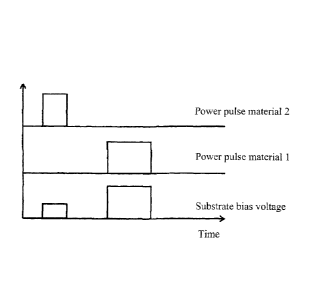
Figure 2 shows the substrate bias synchronized onto the power pulse.
Figure 3 shows diagrammatically a coating facility.
For a better understanding of the complex processes of a HIPIMS method, the
target
poisoning will first be covered in a little more detail. The reactive sputter
process is
determined by the reaction of the target surface with the reactive gas such as
for
example nitrogen or oxygen. This is called target poisoning. When there is a
high
degree of poisoning of the target surface and a high reactivity (e.g.
nitration or
oxidation), this results in a low sputter rate. If in this case the sputter
rate is plotted as
Date Recue/Date Received 2020-08-07
81784887
2b
a function of the reactive gas flow, it thus yields the hysteresis known to
the one
skilled in the art.
Figure 1 shows the absorption of nitrogen at the reactive surfaces such as
target and
layer depending on the ratio of nitrogen flow to argon flow for different
pulse
durations. In this respect, the average pressure and the Ar flow were also
held
constant. The pulse power
CA 2878324 2019-11-27
CA 02878324 2015-01-05
3
W02014008984
was 1000W/cm2. The solid line refers to a pulse duration of 50ps and the
dotted line
relates to a pulse duration of 2000ps.
The characteristic curve of a HIPIMS process with a pulse duration of 50ps
shows, when
nitrogen is added, a complete utilization of the added nitrogen up to a N2/Ar
¨ flow ratio of
approx. 0.9. The nitrogen consumption is more or less proportional to the
coating rate.
From a ratio of 1.0 and higher, the sputter rate falls strongly due to the
nitration of the
target surface. This zone is called transition zone. It marks the area of
transition to a
poisoned target surface. A further addition of nitrogen will cause the target
surface to
become increasingly poisoned and the rate comes near a minimum value.
If the above-mentioned HIPIMS discharge is operated with a pulse duration of
2000ps at
the otherwise same average sputter power, the transition zone shifts to a
poisoned target
surface to higher N2/Ar flow ratios. This, however, means that at a specified
N2/Ar flow
ratio, it is possible by selecting the pulse duration to adjust whether the
sputtering occurs
with a target in metallic mode, in poisoned mode or in the transition zone. In
other words,
the operating point can be adjusted by means of selecting the pulse duration.
This opens
up the possibility, in the case of two or several targets with different
materials and thus
different response patterns vis-a-vis the sputter gas, to adjust a pulse
duration associated
with each target material at their operating point independently from one
another.
It should be noted that when pulsing with moderate power densities, as used in
the
conventional sputtering process, the above-mentioned dependency on the pulse
duration
does not occur.
Figure 1 shows in particular that when the operating point is specified with
the ratio of
reactive gas to inert gas being set at 1.2, the HIPIMS sputter process runs in
the poisoned
mode already when using a pulse duration of 50ps and the coating rate is
approx. 30%
lower than the maximum achievable coating rate in the transition zone. By
increasing the
pulse duration of the HIPIMS power pulse whilst otherwise maintaining a
constant average
CA 02878324 2015-06-12
31812-40
4
sputter power and the same process gas conditions, the operating point
selected with a
reactive gas to inert gas ratio of 1.2 will lie again in the transition zone.
The inventors conjecture that in the frame of the HIPIMS process the decisive
role is
played by the energy quantum per power pulse which results from the product of
the pulse
power amplitude and of the pulse duration. The number of pulses per time unit
can also
= play a role in this respect.
The invention will now be described in detail on the basis of several
embodiments by way
of example and with the aids of the figures.
A coating chamber in which an inventive HIPIMS process is to be used comprises
a first
= sputter source Q1 with a first target TA1 of a first target material to
be sputtered and a
second sputter source Q2 with a second target TA2 of a second target material.
In the
example, the first target TAI can consist of aluminum and the second target
TA2 of
chromium. According to a first embodiment of the present invention, argon and
nitrogen in
a 1:1 ratio are let into the previously evacuated coating chamber. The target
surfaces thus
experience the same reactive and inert gas partial pressure. The power density
applied at
the targets in the pulses is set at 1000W/cm2. The pulse durations (t1, t2)
are set
individually per target in such a manner that the respective operating point
is in the
transition zone. The fill factor D, i.e. the ratio between pulse duration and
repeat interval
(i.e. the time interval from the beginning of a pulse at one target until the
beginning of the
next pulse at the same target) is chosen to be the same for both targets. This
thus results
in a different average output being applied to the targets. The high power
density will result
=
CA 02878324 2015-01-05
W02014008984
in a high ionized proportion of the sputtered material. If a negative bias is
applied to the
substrates to be coated, this yields dense smooth layers.
According to a second embodiment of the present invention, by contrast to the
first
embodiment, the power densities applied at the targets and/or the fill factors
are adjusted
individually.
As is easily understood by the one skilled in the art, the possibility of
providing pulses
having a high power density with a prespecified pulse profile in a controlled
manner plays
an important role in the inventive method. If the power source allows it, the
pulses can be
applied at the targets in a completely independent manner from the respective
other target.
This is in particular the case if a separate power source is allocated to each
target. In this
respect, high-performance DC generators can be used that deliver their output
at the
respective associated target for the pulse duration and for the rest of the
time supply their
output to a so-called power drain (hereinafter called dummy load). Delivering
the output to
a dummy load makes sense especially at the beginning of the output discharge
since the
latter follows a buildup characteristic determined by the generator. Using
several
generators has the disadvantage that a large part of the output, namely the
part that is
channeled onto the dummy loads is simply not used.
According to a new method, it is possible to use in this connection a high-
performance DC
generator whose output is applied to the different targets by means of
switches
sequentially and preferably without interruption of the power delivery. At the
end of the
pulse interval, the power is then simply switched over onto the target. Again,
it may be
beneficial to also switch it at the beginning and/or intermittently onto a
target replacement
(dummy load). However, the loss of power at the dummy load, due to the fact
that power is
applied to several targets sequentially, is very much reduced.
If power is applied to the targets sequentially with power pulses, there is
the possibility
according to a particularly preferred embodiment to synchronize the bias
applied to the
substrates with the pulse sequence and to individually apply a substrate
voltage pulse
CA 02878324 2015-01-05
6
W02014008984
chosen specifically for a target and thus for a layer material. It is thus
possible for example
for another substrate bias voltage and thus acceleration of the ions to occur
for target
material 1 than for target material 2. The corresponding situation is
represented in figure 2.
Coating facilities are often executed as batch systems in which the different
coating
sources are placed on the chamber walls. The substrates to be coated are then
placed in a
so-called carousel in workpiece holders and due to the rotation of the
carousel are
periodically brought past the coating sources. A corresponding situation is
represented by
way of example and schematically in figure 3. With such a structure it can
happen that the
layer thus generated is not deposited as a homogenous mixed crystal but so-
called nano-
layers are produced, wherein from one nano-layer to the neighboring one the
layer
composition changes. Since, as discussed above, the coating rate can be
adjusted
individually for each target by means of the pulse length, the thickness of
the different
nano-layers can be adjusted relatively to one another in a simple manner
according to the
invention.