Note: Descriptions are shown in the official language in which they were submitted.
AMPLIFIED WIDELY TUNABLE SHORT CAVITY LASER
FIELD OF THE INVENTION
[001] The present invention relates to tunable lasers, widely tunable
lasers,
wavelength swept sources, amplified tunable lasers, rapidly tuned lasers, and
optical
systems enabled by these devices.
BACKGROUND
[002] Widely and rapidly tunable lasers are important for a variety of
detection,
communication, measurement, therapeutic, sample modification, and imaging
systems.
For example, swept source optical coherence tomography (SSOCT) systems employ
repetitively swept tunable lasers to generate subsurface microstructural
images of a wide
range of materials. In SS-OCT, wide tuning range translates to higher axial
measurement
resolution, and higher tuning speed enables real-time acquisition of large
data sets. In
= addition, variable tuning speed enables trading off imaging range and
resolution as
required for different applications. Lastly, long coherence length, which is
equivalent to
narrow linewidth, enables long imaging range.
[003] Another example of a system which requires rapidly and
widely tunable
lasers is transient gas spectroscopy as, for example, described in (Stein,
B.A., Jayaraman,
V. Jiang, J.J, et al., "Doppler-limited H20 and HF absorption spectroscopy by
sweeping
the 1321-1354 nm range at 55kHz repetition rate using a single-mode MEMS-
tunable
VCSEL," Applied Physics B: Lasers and Optics 108(4), 721-5 (2012)). In gas
spectroscopy, tuning speed enables characterization of time-varying processes,
such as in
engine thermometry. Narrow spectral width enables resolution of narrow
absorption
features, such as those that occur at low gas
- 1 -
CA 2878975 2019-09-24
CA 02878975 2015-01-09
WO 2014/018939
PCMJS2013/052411
2
temperatures. Other transient spectroscopic applications include monitoring of
explosive
or other non-repetitive processes.
[004] Beyond wide tunability and long coherence length, other important
parameters for tunable lasers for a variety of applications include tuning
speed and
variability of tuning speed. In SS-OCT, increased tuning speed enables imaging
of time-
varying physiological processes, as well as real-time volumetric imaging of
larger data
sets. Also for SS-OCT, variability of tuning speed enables switching between
high
speed, high resolution short-range imaging, and low speed, low resolution long
range
imaging in a single device, which is of great utility in, for example,
ophthalmic imaging,
as described in (Grulkowski, I., Liu, J. J., Potsaid, B. et al., "Retinal,
anterior segment
and full eye imaging using ultrahigh speed swept source OCTwith vertical-
cavity surface
emitting lasers," Biomed. Opt. Express, 3(11), 2733-2751 (2012)).
Spectroscopic or
other detection applications benefit in analogous ways from high-speed and
variable
speed.
[005] Further desirable properties of widely tunable lasers include high
output
power, center wavelength flexibility, spectrally shaped output, monolithic and
low-cost
fabrication, and compatibility with array technology. High power increases
signal to
noise ratio for virtually every application. Center wavelength flexibility
translates into
greater utility in a larger variety of applications. Spectrally shaped output
also increases
signal to noise ratio and improves thermal management. Monolithic, low cost
fabrication
has obvious advantages, and array technology simplifies applications in which
multiple
sources are multiplexed.
[006] The limitations of prior art tunable lasers with respect to the
desirable
properties above can be understood by examination of three representative
examples.
These examples include Fourier Domain mode-locked (FDML) lasers, external
cavity
tunable lasers (ECTL), and sampled grating distributed bragg reflector (SGDBR)
lasers.
An FDML laser is described in (Huber, R., Adler, D. C., and Fujimoto, J. G., -
Buffered
Fourier domain mode locking: unidirectional swept laser sources for optical
coherence
CA 02878975 2015-01-09
WO 2014/018939
PCMJS2013/052411
3
tomography imaging at 370,000 lines/s," Optics Letters, 31(20), 2975-2977
(2006)). Use
of a commercial ECTL in an SSOCT system is described in (George, B., Potsaid,
B.,
Baumann, B., Huang, D. et al., "Ultrahigh speed 1050nm swept source / Fourier
domain
OCT retinal and anterior segment imaging at 100,000 to 400,000 axial scans per
second,"
Optics Express, 18(19), 20029-20048 (2010)). Operation of an SGDBR laser is
described in (Derickson, D., "High-Speed Concatenation of Frequency Ramps
Using
Sampled Grating Distributed Bragg Reflector Laser Diode Sources for OCT
Resolution
Enhancement," Proceedings of the SPIE - The International Society for Optical
Engineering, 7554, (2010)). FDML and ECTL devices are essentially multi-
longitudinal
mode devices, which sweep a cluster of modes instead of a single mode across a
tuning
range. This results in limited imaging range for SSOCT and limited spectral
resolution
for spectroscopic applications. Both FDML and ECTL are also non-monolithic
sources,
which are assembled from discrete components, and therefore not low cost
devices or
compatible with array fabrication. The ECTL further suffers from fundamental
speed
limitations of about 100kHz repetition rate or less, due to the long time
delay in the
external cavity, as described in (Huber, R., Wojtkowski, M., Taira, K. et at.,
"Amplified,
frequency swept lasers for frequency domain reflectometry and OCT imaging:
design and
scaling principles," Optics Express, 13(9), 3513-3528 (2005).) Further speed
limitations
in ECTL devices arise from the large mass of the grating tuning element, as
for example
in the commercially available Thorlabs model SL1325-P16 grating tuned laser.
The
FDML suffers also from inflexiblity of both center wavelength and tuning
speed. Since
the FDML employs a long fiber-based cavity, it can only operate at wavelengths
where
low-loss optical fiber is readily available. Secondly, the FDML sweep rate is
fixed by the
roundtrip time of light in the fiber external cavity, and variable sweep rates
are therefore
not possible in a single devices.
[007] The SGDBR is a single transverse and longitudinal mode device, and
has
the potential for long imaging range and narrow spectral width. Tuning,
however, is
accomplished by discontinuous hopping amongst various modes, which tends to
CA 02878975 2015-01-09
WO 2014/018939
PCMJS2013/052411
4
introduce measurement artifacts. The mode-hopping also requires multiple
tuning
electrodes, complicated drive circuitry and associated speed limitations. The
SGDBR
also suffers from limited tuning range relative to external cavity and FDML
lasers, since
the latter use lossless tuning mcchanicms, while the SGDBR is tuned by free
carrier
injection, which introduces free carrier losses and limits tuning range. The
SGDBR also
suffers from center wavelength inflexibility, due to the need for complex
regrowth
fabrication technology which is only mature in the Indium Phosphide material
system.
[008] The problems discussed above with respect to the FDML, ECTL, and
SGDBR above are representative of problems encountered by most tunable lasers
known
in the art.
[009] MEMS-tunable vertical cavity lasers (MEMS-VCSELs) offer a potential
solution to the problems above. The short cavity of MEMS-VCSELs leads to a
large
longitudinal mode spacing and relative immunity to mode hops. The MEMS-VCSEL
requires only one tuning electrode to sweep a single mode across the tuning
range, and
therefore offers the promise of long SS-OCT imaging range with minimal
measurement
artifacts, and rapid tuning. The short cavity and the short mass of the MEMS
mirror offer
the potential for very high speed. MEMS-VCSEL technology can also be extended
to a
large variety of wavelength ranges difficult to access with many other types
of sources,
making them appropriate for other types of spectroscopic, diagnostic, and
detection
systems. The application of MEMS-VCSELs to SS-OCT imaging was first described
in
US patent 7468997. MEMS-VCSELs have the potential for wide tuning range, as
discussed in US patent 7468997. Until 2011, however, the widest MEMS-VCSEL
tuning
range achieved was 65 nm around 1550 nm, as described in (Matsui, Y.,
Vakhshoori, D.,
Peidong, W. et al., "Complete polarization mode control of long-wavelength
tunable
vertical-cavity surface-emitting lasers over 65-nm tuning, up to 14-mW output
power,"
IEEE Journal of Quantum Electronics, 39(9), 1037-10481048 (2003). This
represents a
fractional tuning range of about 4.2%, or about a factor of 2 less than that
required in SS-
OCT imaging.) In 2011, a tuning range of 111 nm was demonstrated in a 1310 nm
CA 02878975 2015-01-09
WO 2014/018939
PCMJS2013/052411
MEMS-VCSEL, which was subsequently applied in an SSOCT imaging system, as
described in (Jayaraman, V., Jiang, J., Li, H. et al., "OCT Imaging up to 760
kHz Axial
Scan Rate Using Single-Mode 1310nm MEMS-Tunable VCSELs with >100nm Tuning
Range," CLEO: 2011 - Laser Science to Photonic Applications, 2 pp.-2 pp.2 pp.
(2011).)
10101 The MEMS-VCSEL described by Jayaraman, et al. in 2011 represented a
major innovation in widely tunable short cavity lasers. Achieving peformance
and
reliablity appropriate for commercial optical systems, however, requires
optimization of
tuning speed, frequency response of tuning, tuning range, spectral shape of
tuning curve,
output power vs. wavelength, post-amplified performance, gain and mirror
designs, and
overall cavity design. Numerous design innovations are required to improve
upon the
prior art to achieve performance and reliability necessary for these
commercial systems.
10111 From the foregoing, it is clear that what is required is a widely
tunable
short-cavity laser with 3-dimensional cavity and material design optimized for
performance and reliability in SSOCT imaging systems, spectroscopic detection
systems
and other types of optical systems.
SUMMARY
[012] This document provides several preferred embodiments of a tunable
source comprising a short-cavity laser optimized for performance and
reliability in
SSOCT imaging systems, spectroscopic detection systems, and other types of
detection
and sensing systems. This document presents a short cavity laser with a large
free
spectral range cavity, fast tuning response and single transverse,
longitudinal and
polarization mode operation. The disclosure includes embodiments for fast and
wide
tuning, and optimized spectral shaping. Preferred embodiments include both
electrical
and optical pumping in a MEMS-VCSEL geometry with mirror and gain regions
optimized for wide tuning, high output power, and a variety of preferred
wavelength
ranges. Other preferred embodiments include a semiconductor optical amplifier,
combined with the short-cavity laser to produce high-power, spectrally shaped
operation.
CA 02878975 2015-01-09
WO 2014/018939
PCMJS2013/052411
6
Several preferred imaging and detection system embodiments make use of this
tunable
source for optimized operation.
[013] One embodiment provides an amplified tunable laser source, comprising
input tunable radiation with an input power spectrum, an input center
wavelength, input
wavelength range and input average power, optically coupled to an input side
of a
semiconductor optical amplifier comprising at least one quantum well, and
output tunable
radiation having an output power spectrum, an output center wavelength, an
output
wavelength range, and output average power, emerging from an output side of
said
optical amplifier, wherein said input tunable radiation is generated by a
tunable laser
comprising: an optical cavity including a first and second mirror; a gain
region interposed
between said first and second mirrors; a tuning region; and means for
adjusting an optical
path length of said tuning region; wherein: a free spectral range (FSR) of
said optical
cavity exceeds 5% of said center wavelength; said tunable laser operates
substantially in
a single longitudinal and transverse mode over said wavelength range; and said
means for
adjusting an optical path length has a wavelength tuning frequency response
with a 6-dB
bandwidth greater than about 1 kHz.
[014] Another embodiment provides an amplified tunable laser source,
comprising input tunable radiation with an input power spectrum, an input
center
wavelength, input wavelength range and input average power, optically coupled
to an
input side of a fiber-based optical amplifier comprising at least one quantum
well, and
output tunable radiation having an output power spectrum, an output center
wavelength,
an output wavelength range, and output average power, emerging from an output
side of
said optical amplifier, wherein said input tunable radiation is generated by a
tunable laser
comprising: an optical cavity including a first and second mirror; a gain
region interposed
between said first and second mirrors; a tuning region; and means for
adjusting an optical
path length of said tuning region; wherein: a free spectral range (FSR) of
said optical
cavity exceeds 5% of said center wavelength; said tunable laser operates
substantially in
a single longitudinal and transverse mode over said wavelength range; and said
means for
CA 02878975 2015-01-09
WO 2014/018939
PCMJS2013/052411
7
adjusting an optical path length has a wavelength tuning frequency response
with a 6-dB
bandwidth greater than about 1 kHz.
BRIEF DESCRIPTION OF THE DRAWINGS
[015] Figure 1 illustrates an embodiment of widely tunable short cavity
laser
according to an embodiment.
[016] Figure 2 illustrates an output power spectrum of a widely tunable
short-
cavity laser.
[017] Figure 3 illustrates the definition of free spectral range.
[018] Figure 4 shows a water vapor absorption spectrum in the 1330-1365 nm
rang.
[019] Figure 5 shows a measurement dynamic coherence length obtained by the
rolloff of the OCT point spread function vs. imaging depth.
[020] Figure 6 illustrates an embodiment of a widely tunable short-cavity
laser
with closed loop control.
[021] Figure 7 illustrates a MEMS-VCSEL implementation of a tunable short
cavity laser operating near 1310 urn.
[022] Figure 8 illustrates an axial refractive index profile of a short
cavity laser
having 4 standing wave maxima between two minors of the cavity.
[023] Figure 9 illustrates the static and dynamic tuning response of the
MEMS-
VCSEL illustrated in Fig. 7.
[024] Figure 10 illustrates a variety of MEMS-VCSEL actuator frequency
responses.
[025] Figure 11 illustrates a widely tunable short-cavity laser with piezo
tuning.
[026] Figure 12 illustrates various actuator geometries.
[027] Figure 13 illustrates oxidation for a fully oxidized minor proceeding
from
two etched holes.
CA 02878975 2015-01-09
WO 2014/018939
PCMJS2013/052411
8
[028] Figure 14 illustrates a 1310 nm reflectivity spectrum configured to
support
pumping at 1050 nm.
[029] Figure 15 illustrates an embodiment of a widely tunable short cavity
laser
coupled to an optical amplifier.
[030] Figure 16 illustrates an ASE spectrum from a dual-quantum state
semiconductor optical amplifier.
[031] Figure 17 illustrates a widely tunable short cavity laser coupled to
an
optical amplifier, the output of which is coupled to a synchronously tuned
optical filter.
[032] Figure 18 illustrates an amplified widely tunable short cavity laser
with a
tunable optical filter between the laser and amplifier.
[033] Figure 19 illustrates an embodiment of a widely tunable short cavity
laser
with two amplification stages.
[034] Figure 20 illustrates an embodiment of a widely tunable short cavity
laser
with two amplification stages and a tunable optical filter between the stages.
[035] Figure 21 illustrates an amplified and pre-amplified spectrum of a
widely
tunable short cavity laser.
[036] Figure 22 illustrates various output power spectra of a widely
tunable
short-cavity laser operating near 1310 nm.
[037] Figure 23 illustrates a MEMS-VCSEL implementation of a widely tunable
short-cavity laser operating near 1060 nm.
[038] Figure 24 illustrates static and dynamic tuning spectra of the MEMS-
VCSEL in Figure 23.
[039] Figure 25 illustrates steps 1-4 in the fabrication of a widely
tunable short
cavity laser realized as a MEMS-VCSEL.
[040] Figure 26 illustrates steps 5-6 in the fabrication of a widely
tunable short
cavity laser realized as a MEMS-VCSEL.
[041] Figure 27 illustrates an electrically pumped MEMS-VCSEL
implementation of a widely tunable short-cavity laser.
CA 02878975 2015-01-09
WO 2014/018939
PCMJS2013/052411
9
[042] Figure 28 illustrates wavelength sweeps from two short-cavity lasers
interleaved to produce a multiplied sweep rate.
DETAILED DESCRIPTION
[043] The description of illustrative embodiments according to principles
of the
present invention is intended to be read in connection with the accompanying
drawings,
which are to be considered part of the entire written description. In the
description of
embodiments of the invention disclosed herein, any reference to direction or
orientation
is merely intended for convenience of description and is not intended in any
way to limit
the scope of the present invention. Relative terms such as "lower," "upper,"
"horizontal,"
"vertical," "above," "below," "up," "down," "top" and "bottom" as well as
derivative
thereof (e.g., "horizontally," "downwardly," "upwardly," etc.) should be
construed to
refer to the orientation as then described or as shown in the drawing under
discussion.
These relative terms are for convenience of description only and do not
require that the
apparatus be constructed or operated in a particular orientation unless
explicitly indicated
as such. Terms such as "attached," "affixed," "connected," "coupled,"
"interconnected,"
and similar refer to a relationship wherein structures are secured or attached
to one
another either directly or indirectly through intervening structures, as well
as both
movable or rigid attachments or relationships, unless expressly described
otherwise.
Moreover, the features and benefits of the invention are illustrated by
reference to the
exemplified embodiments. Accordingly, the invention expressly should not be
limited to
such exemplary embodiments illustrating some possible non-limiting combination
of
features that may exist alone or in other combinations of features; the scope
of the
invention being defined by the claims appended hereto.
[044] This disclosure describes the best mode or modes of practicing the
invention as presently contemplated. This description is not intended to be
understood in
a limiting sense, but provides an example of the invention presented solely
for illustrative
purposes by reference to the accompanying drawings to advise one of ordinary
skill in the
CA 02878975 2015-01-09
WO 2014/018939
PCMJS2013/052411
art of the advantages and construction of the invention. In the various views
of the
drawings, like reference characters designate like or similar parts.
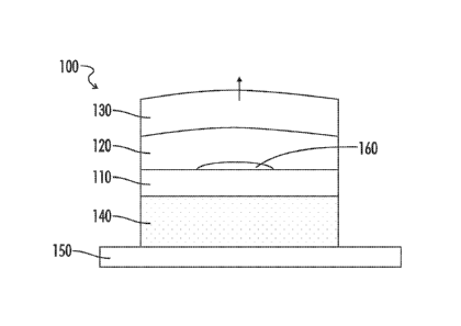
[045] Figures 1-3 illustrate properties of a preferred embodiment of a
short-
cavity tunable laser in accordance with the present invention. As shown in
Fig. 1, the
laser 100 comprises a gain region 110 and a tuning region 120, interposed
between a first
mirror 130 and a second mirror 140. Energy to support lasing operation can be
supplied
to the gain region in the form of optical or electrical pumping, as is well-
known to those
skilled in the art of lasers. A thermally conductive heat spreading layer 150,
preferably a
metal such as gold, gold-tin, indium, or indium containing solder adjacent one
mirror can
also be employed to increase an average output power of the tunable short
cavity laser.
In the case of a vertical cavity laser on a GaAs substrate, for example, a
substrate via
could be etched, stopping on the second mirror, on which the heat-spreading
layer could
be deposited through the substrate via.
[046] Referring to Fig. 1, adjustment of the effective optical path length
of the
tuning region causes the wavelength of the laser to be tuned. The laser emits
wavelength
tunable radiation, which is emitted through the first mirror. A typical
emitted power
spectrum 200, which is the power emitted as a function of wavelength, as shown
in Fig.
2. The Spectrum represents range of wavelengths in tunable emission and
intensity at
each wavelength. The wavelength tunable emission spans a wavelength emission
range
210 having a center wavelength 220. In the preferred embodiment of Fig. 1, the
tuning
region is an adjustable airgap, but other embodiments such as a liquid crystal
or
semiconductor whose optical path can be modified by adjustment of the
refractive index
are also possible.
[047] A preferred embodiment of the short-cavity tunable laser of Fig. 1 is
a
vertical cavity laser (VCL), but other embodiments, including but not limited
to short-
cavity edge-emitting lasers, could be employed. As is well-known to those
skilled in the
art of vertical cavity lasers, the VCL can be fabricated in monolithic one and
two-
dimensional arrays, which is advantageous for optical systems requiring
multiple optical
CA 02878975 2015-01-09
WO 2014/018939
PCMJS2013/052411
11
sources. Modern wafer scale optical fabrication techniques would allow for the
precise
location of such an array of laser emitters, as well as optical components
which would
then support the manufacturing of optical instruments from these arrays.
[048] The short cavity employed in an embodiment results in a large free-
spectral range (FSR), which is inversely related to cavity length. The present
embodiment discloses an FSR which in the present invention is >5% of the
center
wavelength shown in Fig. 2. As shown in Fig. 3, free spectral range is defined
as the
distance between transmission peaks, or longitudinal modes, in the direction
of laser
oscillation, of the optical cavity defined by the layers of Fig. 1. The
maximum
continuous mode-hop-free single-mode tuning range of the tunable laser is
limited by the
FSR. Thus, a laser having an FSR that is 5% of the center wavelength can be
expected to
have a maximum tuning range that is 5% of the center wavelength. Other
considerations,
such as the maximum achievable change in optical path length of the tuning
region, or the
available gain bandwidth of the gain region may limit the continuous single
mode tuning
range to less than the FSR, but the FSR represents an upper limit.
[049] In the preferred embodiment, an anti-reflection coating is placed
between
the gain region and the tuning region to suppress reflections in the device
and extend the
tuning range. This anti-reflection coating can be a quarter wavelength of
material such as
silicon nitride or silicon oxynitride, in the preferred case when the tuning
region is air,
and the gain region is semiconductor.
[050] Fig. 1 also illustrates that the top mirror 130 can be curved to form
a half-
symmetric cavity as in (Tayebati, P., Wang, P., Vakhshoori, D. et al., "Half-
symmetric
cavity tunable microelectromechanical VCSEL with single spatial mode," IEEE
Photonics Technology Letters, 10(12), 1679-1681 (1998)), which includes one
curved
mirror and one flat mirror. This is important because, although the short
cavity and large
FSR promote single longitudinal operation, the curved mirror further promotes
single
transverse mode operation, which is important for applications in imaging and
spectroscopy. The function of the curved mirror can also be accomplished by an
intra-
CA 02878975 2015-01-09
WO 2014/018939
PCMJS2013/052411
12
cavity microlens 160, as shown in Fig. 1. Generally either the microlens 160
or the
curved mirror 130 can be used, but a combination of both can also be used. The
microlens can be formed by reflow of a resist or polymer material, followed by
pattern
transfer of that shape into underlying materials, as is described in
(Strzelecka, E. M.,
Robinson, G. D., Coldren, L. A. et al., "Fabrication of refractive microlenses
in
semiconductors by mask shape transfer in reactive ion etching,"
Microelectronic
Engineering, 35(1-4), 385-388 (1997)) and known to those who are skilled in
the art.
Similarly, the curved mirror can be formed by structuring of sacrificial layer
by a reflow
and pattern transfer technique, deposition of the top mirror, and removal of
the sacrificial
layer. The sacrificial layer in such a process is preferably silicon or
germanium, and the
pattern transfer of a reflowed resist layer can be accomplished by inductively
coupled
plasma etching using a CF4/oxygen gas mixture. The curvature of the resulting
surface
in the sacrificial layer is a function of the ratio of these gases, and can be
adjusted by
straightforward optimization of this ratio.
[051] Achieving single transverse-mode operation of the tunable short
cavity
laser in Fig. 1 requires careful control of the curved mirror radius of
curvature and the
combined thickness of gain region and tuning region between the two minors.
For the
case of an airgap tuning region and operation near 1310 nm using a
semiconductor gain
region comprised of InP-based materials, typical dimension are a gain region
thickness
of about 1 micron, airgap thickness of about 1.6 pm, and a mirror radius of
curvature of
around 1 mm. Those skilled in the art of laser fabrication and design can
adjust numbers
in this range to achieve more specific numbers for particular designs in
particular
wavelength regimes. Using parameters close to these will lead to single
longitudinal and
transverse mode suppression of 40-50 dB.
[052] The single longitudinal and transverse mode operation achieved by the
short cavity laser according to an embodiment enables an optical source with
very long
dynamic coherence length. This coherence length is in excess of 100 mm under
dynamic
operation. Coherence length is inversely related to laser line-width. Long
coherence
CA 02878975 2015-01-09
WO 2014/018939
PCMJS2013/052411
13
length is important in spectroscopic applications requiring the measurement of
narrow
spectral features. In imaging applications like swept source optical coherence
tomography (SS-OCT), long coherence length corresponds to long imaging range.
Figure 5 shows a detection-limited measurement of coherence length in an SS-
OCT
system, obtained by repetitive sweeping at 60 kHz of a tunable laser according
to Fig. 1,
in which the FSR is about 8-9% of the center wavelength, and using the OCT
point
spread function as a measurement of coherence length. The absence of
substantial
amplitude degradation at 50 mm indicates that the coherent length is greater
than 100
mm. This measurement method is well-known to those skilled in the art of SS-
OCT.
[053] For some applications, it is advantageous to reduce the coherence
length to
eliminate interference from unwanted reflections in an optical system.
Coherence length
can be adjusted by adding a noise waveform to the tuning region, or otherwise
amplitude
or phase modulating the source. External means could include, for example, a
temporal
diffuser.
[054] In an embodiment, the frequency response of the optical path length
of a
tuning region to an applied tuning signal has a 6-dB bandwidth that exceeds
about 1 kHz.
Normally, this 6-dB bandwidth starts at DC but can start at some non-zero
frequency as
well. The 1 kHz bandwidth distinguishes the present invention from other types
of tuning
mechanisms employed in the prior art, such as electro-thermal tuning in
(Gierl, C.,
Gruendl, T., Debernardi, P. et al., "Surface micromachined tunable 1.55 mu m-
VCSEL
with 102 nm continuous single-mode tuning," Optics Express, 19(18), 17336-
17343
(2011)). In the preferred case where the tuning region is an airgap, the
airgap can be
tuned by a MEMS-based actuator, which contracts the airgap through
electrostatic force.
MEMS-based tuning mechanisms have been demonstrated to have a 6-dB bandwidth
exceeding 500 kHz, as illustrated in (Jayaraman, V., Cole, G. D., Robertson,
M. et al.,
"High-sweep-rate 1310 nm MEMS-VCSEL with 150 nm continuous tuning range,"
Electronics Letters, 48(14), 867-9 (2012)). As described below, the bandwidth
of a
MEMS-actuator can be extended to >1 MHz. The presence of such a wide bandwidth
CA 02878975 2015-01-09
WO 2014/018939
PCMJS2013/052411
14
enables repetitively swept operation at a range of frequencies from DC to >1
MHz. It
also enables non-repetitive wavelength tuning at a variety of scan speeds. The
ability to
vary the fundamental tuning frequency of the laser within one laser source
makes the
instrument appropriate for a broad range of applications, each of which have a
preferred
tuning rate. For example, the measurement of weak spectroscopic signals could
require
slow scanning speeds, whereas strong spectroscopic signals could be monitored
such that
dynamic temporal effects could be captured. Many applications in SSOCT could
also
benefit from variable scan frequency, which enables tradeoff of imaging
resolution and
imaging range with imaging speed.
[055] Although MEMS tuning of an airgap is the preferred embodiment of the
present invention, an alternative embodiment could tune the airgap through a
piezo-
electric actuator, such as described by (US patent 6263002). This
configuration is
illustrated also in Fig. 11, where the top mirror 1110 is placed on a piezo-
electric actuator
and separated by an airgap 1120 from the gain region 1130 and the bottom
mirror 1140.
The first mirror 1110 is moved relative to the gain region 1130 via piezo-
electric control
changing the airgap 1120 tuning region and therefore, the lasing wavelength.
In this
structure, the first mirror is attached to a fiber that can deliver pump
radiation and collect
laser radiation. Piezo tuning can also provide several kHz of bandwidth, which
is
generally less than the bandwidth of MEMS tuning, but piezo tuning can produce
larger
airgap changes, and can be bi-directional. It is also possible to obtain bi-
directional
tuning in a MEMS device through a 3-terminal device. In yet another
embodiment, piezo
and MEMS tuning can both be used to provide a combination of a slower, large
stroke
tuning mechanism, and a faster, small stroke tuning mechanism. These tuning
mechanisms can be combined further with other tuning mechanisms such as
carrier
injection tuning in semiconductors.
[056] The tuning region can be driven with a variety of waveforms, to
generate
various wavelength trajectories vs. time out of the short-cavity laser for a
variety of
applications. For example, the tuning region can be driven with a repetitive
waveform
CA 02878975 2015-01-09
WO 2014/018939
PCMJS2013/052411
having a fundamental frequency, generating a periodic variation of wavelength
vs. time
for applications such as swept source optical coherence tomography (SSOCT).
The
periodic waveform could be sinusoidal in shape, or an arbitrary waveform
constructed to
generate a linearized wavelength sweep vs. time or any wavelength trajectory
with time.
The response of the tuning region may be non-linear with respect to the
applied
waveform. A classic example is MEMS, in which the movement of an
electrostatically
actuated membrane varies as the square of applied voltage. In this case,
creating a linear
movement requires pre-distorting the applied waveform to account for the non-
linear
response of the MEMS actuator. The generation of arbitrary waveforms to
linearize
MEMS response is well-known to those skilled in the art of driving MEMS
devices, but
the principle of linearization can be applied to other tuning mechanisms as
well.
[057] The waveform applied to the tuning region is usually a variation in
applied
voltage or current vs. time, depending on the exact nature of the tuning
region and
mechanism of tuning, whether it be changing a physical path length or changing
a
refractive index of a semiconductor or liquid crystal, as some representative
examples.
By way of example, use of a MEMS based tuning element with its very low mass
reduces
the power required to sweep the laser wavelength in both a continuous sweep as
well as
in a non-continuous sweep. The use of a MEMS tuning element would require a
drive
voltage with very little current drawn.
[058] In addition to repetitive wavelength sweeping, the tuning region can
be
driven by a non-repetitive waveform, in response to an external trigger, or by
any
repetitive or non-repetitive arbitrary waveform. Examples of this are in
transient
spectroscopy, where it is advantageous to measure the transmission,
absorption, or
reflection spectrum of a material shortly after an event, such as an
explosion, chemical
reaction, or a biological event. Non-repetitive scanning would also facilitate
new modes
of operation whereby a number of narrow regions of interest separated by large
regions of
no interest could be interrogated with the laser in an optimized manner. One
example is a
series of slow scans across narrow spectroscopic features that are separated
by large
CA 02878975 2015-01-09
WO 2014/018939
PCT/US2013/052411
16
regions wherein the large regions are scanned at high speed. In the preferred
case of
MEMS tuning, many new operating modes are made possible by the extremely low
mass
of the tuning element that allows for rapid acceleration and deceleration of
the laser
tuning speed.
[059] With respect to scanning in response to an external trigger, the
advantages
of a MEMS implementation of the present invention are illuminated by a
comparison
with the commercially available Thorlabs model SL1325-P16 swept source laser
(which
is not a short-cavity laser). This prior art laser utilizes a resonantly
scanned optical
grating measuring over 10 mm2 as the tuning element, causing slow response
time
relative to a low mass MEMS element in the present invention. In an embodiment
according to the present invention the very low mass of the tuning element
allows greater
flexibility in the operating parameters, such as how quickly the laser can
respond to an
external event, as well as the wavelength region over which the laser is tuned
as a result
of an external event. This flexibility provides new modes of operation when it
is
desirable to synchronize the operation of the laser with external events.
[060] Having the laser tune across a widely adaptable tuning profile allows
the
performance of the laser to be adjusted to meet the demands of many
applications. By
way of example, in one application it would be desirable to scan the
wavelength of the
laser linearly in time if the laser is being used to measure the wavelength
dependence of
an optical element, in other applications would be desirable to scan the laser
linearly in
optical frequency when the laser is being employed to make measurements that
are best
made with samples equally spaced in frequency, such as is the case in Optical
Coherence
Tomography.
[061] Spectroscopy provides another example of the utility of a highly
flexible
tuning profile. In many spectroscopic applications, it is necessary to measure
multiple
unequally spaced and variable linevvidth lines across a range of wavelengths.
Maximizing overall signal to noise ratio requires slower scan speeds in
information rich
(e.g. many narrow lines) regions of the spectrum and faster scan speeds in
regions of the
CA 02878975 2015-01-09
WO 2014/018939
PCMJS2013/052411
17
spectrum with less or no information. Fig. 4 shows an example of a water vapor
absorption spectrum in the 1330-1365 nm range.
[062] For many applications, such as those described above, the tuning
region of
the tunable short-cavity laser according the present region can be driven open
loop¨that
is, without position or wavelength feedback. In other applications where
wavelength
stability is more important, however, feedback control can be employed. This
can be
advantageous in static operation, when the wavelength is locked to a
particular atomic
absorption line or other atomic reference. Alternately, the wavelength can be
first locked
to an atomic reference and then offset from this reference using another
element to
measure the offset distance, such as a Fabry-Perot or Mach-Zehnder
interferometer
having a known fringe spacing. Closed loop control can also be advantageous in
dynamic operation.
[063] Fig. 6 shows a preferred embodiment of closed loop control according
to
the present invention. As shown, a portion of the light emitted from the
tunable short-
cavity laser is split to a wavelength-sensing element 610, which can comprise
elements
such as a prism, grating, optical filter, or optical interferometer. In the
case of a
dispersive element like a prism or a grating, a position-sensing element like
a detector
array would be combined with the dispersive element to detect diffracted or
refracted
angle and infer wavelength offset from the desired position and feed this
error signal to
the tuning drive waveform 620. If the application doesn't require a specific
wavelength
but just that a fixed wavelength, or a series of fixed wavelengths be
delivered, then the
wavelength dispersing element and the position sensing element could be used
without
calibration of the dispersing element. In the case of an optical filter, the
transmission or
reflection of the filter as measured by an optical detector would be used to
determine
wavelength offset from a desired lock position and feed an error signal back
to the tuning
region drive waveform. Dynamic closed loop operation can be obtained by
scanning the
error signal, as has been shown in prior art lasers, such as Figure 1 of
(Roos, P. A.,
Reibel, R. R., Berg, T. et at., "Ultrabroadband optical chirp linearization
for precision
CA 02878975 2015-01-09
WO 2014/018939
PCMJS2013/052411
18
metrology applications," Optics Letters, 34(23), 3692-3694 (2009).) Closed
loop control
is particularly useful when driving a tuning region at speeds well below a
natural
resonance, which may create variabilities. For example, a MEMS actuator with a
500
kHz resonance driven at 100 kHz may be prone to variability and may have much
more
well-behaved tuning with closed loop control.
[064] Fig. 7 illustrates several details of a preferred implementation of
a short-
cavity laser constructed to operate at 1310 nm according to an embodiment of
the present
invention, and Figs. 9 and 10 demonstrate several additional performance
features of the
implementation of Fig. 7. Fig. 7 illustrates a semiconductor laser constructed
as a
vertical cavity surface emitting laser (VCSEL), which is a subset of vertical
cavity lasers
(VCL). A VCL can emit either downward or upward, and VCSELs emit upward,
meaning in the direction opposite the substrate. The VCSEL of Fig. 7 employs
two
distributed Bragg reflector (DBR) mirrors 710, 720 comprising alternating
quarter wave
layers of low and high refractive index material. The DBR is preferred for
both mirrors,
although a high contrast grating as used by prior art lasers can also be
employed, as
described in for example (Chase, C., Rao, Y., Hofmann, W. et al., "1550 nm
high
contrast grating VCSEL," Optics Express, 18(15), 15461-15466 (2010)).
[065] The bottom mirror 710 of Fig. 7, corresponding to the second mirror 140
of Fig. 1, is comprised of alternating quarter wave layers of GaAs and
Aluminum oxide
(Alx0y). This type of mirror is formed by lateral oxidation of an epitaxially
grown stack
of GaAs/AlAs, as described in (MacDougal, M. H., Dapkus, P. D., Bond, A. E. et
al.,
"Design and fabrication of VCSELs with Al x0 y-GaAs DBRs," IEEE Journal of
Selected Topics in Quantum Electronics, 3(3), 905-915915 (1997)). The
GaAs/A1x0y
mirror has a large reflectivity and wide bandwidth with a small number of
mirror periods.
The preferred number of mirror periods for the back mirror, when light is
coupled out the
top mirror as in Fig. 7, is six or seven periods, creating a theoretical
lossless reflectivity
of >99.9%. Other implementations of this minor could use AlGaAs/Alx0y, where
the
aluminum content of the AlGaAs is less than about 92%, so that it does not
oxidize
CA 02878975 2015-01-09
WO 2014/018939 PCMJS2013/052411
19
appreciably during lateral oxidation of the AlAs to form Alx0y. Use of AlGaAs
instead
of GaAs for the low index material is advantageous for increasing the bandgap
of the
low-index material to make it non-absorbing at the lasing wavelength or at the
pump
wavelength if the laser is optically pumped.
[066] The top suspended mirror 720 of Fig. 7, corresponding to the first
mirror
130 of Fig. 1, is comprised of alternating low and high refractive index
deposited
materials, such as for example SiO2 and Ta205. Other deposited materials could
be used
as well, including but not limited to the list consisting of TiO2, Hf02, Si,
Ag, Al, Au,
ZnS, ZnSe, CdF2, Al2F3, and CdS. These materials can be deposited by electron
beam
evaporation, ion beam sputtering, plasma-assisted deposition, or other means
well-known
to those skilled in the art. For the example, in case of a 10 period SiO2/
Ta205 period
mirror having refractive indices of 1.46/2.07 respectively, centered in a
range of about
700 nm to about 1600 nm, the theoretical lossless reflectivity exceeds 99.5%
over a range
of at least 10% of the center wavelength, as can be calculated by those
skilled in the art of
mirror design.
[067] The implementation of Fig. 7 uses MEMS actuation to control the
thickness of an airgap tuning region to control the output wavelength of the
device in the
range of 1310 nm. Application of a voltage between the actuator contacts 730,
740
shown contracts the airgap and tunes the laser to shorter wavelengths. The
MEMS
structure shown consists of a rigid supporting structure 750 and a suspended
deformable
dielectric membrane 760, on which is the suspended top mirror 720. The top of
the
dielectric membrane 760 is metallized to enable electrostatic force to be
applied by the
actuator contacts 730, 740. The membrane itself is transparent, runs
underneath and is
integral with the suspended mirror, and contributes constructively to the
reflectivity of
the suspended mirror. Ideally the membrane thickness is an odd number of
quarter
wavelengths at the center wavelength of the emitted tuned radiation. For many
wavelengths of interest, such as in the 600-2500 nm range, the ideal thickness
is about %
wavelength.
CA 02878975 2015-01-09
WO 2014/018939
PCMJS2013/052411
[068] In the preferred embodiment, the dielectric membrane is silicon nitride,
which is a robust material, which can be stress-engineered to create the
desired frequency
response. Ideally the silicon nitride has a tensile stress in the range or
about 100 to about
1000 MPa. This range of stress leads to a lowest order resonant frequency of
the MEMS
actuator, described below, that is substantially increased by the stress.
Although tensile
stress is preferred, compressive can also be employed, though it is less
preferred, since it
leads to bowing of the membrane after MEMS release. Other authors have made
advantageous use of this bowing to create a half-symmetric cavity, as
described for
example in (Matsui, Y., Vakhshoori, D., Peidong, W. et al., "Complete
polarization mode
control of long-wavelength tunable vertical-cavity surface-emitting lasers
over 65-nm
tuning, up to 14-mW output power," IEEE Journal of Quantum Electronics, 39(9),
1037-
10481048 (2003)).
[069] The representative preferred embodiment is shown in Fig. 7 is configured
to operate at 1310 nm. This configuration therefore uses an InP-based multi-
quantum
well (MQW) region comprising at least one quantum well in the gain region.
Since the
bottom fully oxidized GaAs/A10y mirror is grown on GaAs instead of InP, the
InP-based
MQW region must be joined to the GaAs-based fully oxidized mrror through a
wafer
bonding process, as described in fixed wavelength 1310 nm VCSELs such as in
(Jayaraman, V., Mehta, M., Jackson, A. W. et al., "High-power 1320-nm wafer-
bonded
VCSELs with tunnel junctions," IEEE Photonics Technology Letters, 15(11), 1495-
14971497 (2003)). The multi-quantum well region is preferably comprised of
multiple
compressively strained AlInGaAs quantum wells, with strain in a range of 1-
1.5%. In
another embodiment, it is possible to use a GaInNAs quantum well that can emit
around
1310 nm and can be grown on GaAs, eliminating the need for wafer bonding. The
AlInGaAs quantum well is however higher gain and more wavelength flexible, and
is
therefore preferred.
[070] Figs. 25 and 26 illustrate the major steps of a fabrication sequence
used to
fabricate the preferred implementation of the 1310 nm tunable short cavity
laser in Fig. 7.
CA 02878975 2015-01-09
WO 2014/018939
PCMJS2013/052411
21
Processing of devices in a wavelength range of 650-2300 nm can proceed in a
similar
fashion, with the except that GaAs-based devices do not require the first
wafer bonding
step shown in Fig. 25, since mirror and gain region can be epitaxially grown
in one step.
As shown in Fig. 25, at 1310 nm, or at any wavelength employing an active
region grown
on InP, the first step 2510 involves wafer bonding of the MQW region
epitaxially grown
on an InP substrate to a GaAs/AlAs mirror structure cpitaxially grown on a
GaAs
substrate. This process can be accomplished throught the application of
pressure and
about 570C temperature for about 15 minutes, as has been described in greater
detail by
prior art researchers in (Black, A., Hawkins, A. R., Margalit, N. M. et al.,
"Wafer fusion:
Materials issues and device results," IEEE Journal of Selected Topics in
Quantum
Electronics, 3(3), 943-951 (1997)). The MQW and the mirror structure are
joined at a
wafer-bonded interface. After bonding, the InP substrate is removed in a
second step
2520 using an HCL-based etch stopping on an InGaAs stop etch layer. A sulfuric
acid
based etch then removes the stop-etch layer.
[071] In a third series of steps 2530, the bottom MEMS contact, which is
preferably terminated with titanium to promote adhesion of germanium in a
subsequent
step, and anti-reflection coating are deposited and patterned, and holes are
etched for
oxidation of the GaAs/AlAs mirror structure. Oxidation converts the AlAs to
AlõOy to
create a highly reflecting mirror with six or severn periods. After mirror
oxidation, a
germanium sacrifical layer is deposited in a fourth step 2540, and the
germanium is
structured to have a curved surface in the region of light oscillation. This
curved surface
is created by a photoresist reflow and pattern transfer process, using an
oxygen-rich
CF4/02 inductively coupled plasma etch process. Fig. 26 illustrates how in a
5th series of
steps 2550, the silicon nitride membrane layer, top actuator contact, and top
suspended
mirror are deposited and patterned on the germanium sacrificial layer. The top
contact
layer is preferably aluminum.
[072] In a 6th series of steps 2560, the germanium sacrificial layer is
released
using Xenon Diflouride (XeF2) gas to create a suspended structure with a rigid
CA 02878975 2015-01-09
WO 2014/018939
PCMJS2013/052411
22
germanium support structure at the edges. Prior to the germanium release, wire
bond
pads, shown in Fig. 7 connecting with the top and bottom actuator metal, are
deposited to
complete processing before release. Processing after release is generally not
advisable, as
it can lead to collapse of the actuator. In many cases, it is preferable to
dice and wire
bond devices to a submount for packaging, prior to releasing the germanium
membrane.
[073] The design of the gain region in the preferred embodiment of Fig. 7 is
important for device performance. In the case where the structure is optically
pumped,
the quantum wells can be aligned with peaks of an optical standing wave to
enhance gain
through the well-known periodic gain effect, described in the prior art by
(Corzine, S. W.,
Geels, R. S., Scott, J. W. et al., "DESIGN OF FABRY-PEROT SURFACE-EMITTING
LASERS WITH A PERIODIC GAIN STRUCTURE," IEEE Journal of Quantum
Electronics, 25(6), 1513-1524 (1989)). One further advantage of periodic gain
is that the
wide spacing between quantum wells prevents strain accumulation and reduces
the need
for strain compensation. The ideal pump wavelength for the 1310 nm tunable
VCSEL
shown is in a range of about 850-1050 nm. In an optically pumped structure,
three
quantum wells can be placed on three separated standing wave peaks, and the
region
between them can be made of AlInGaAs substantially lattice-matched to InP, and
of a
composition that absorbs incoming pump radiation. Thus the gain region is
separated
from the absorbing regions, and photo-generated carriers in the absorbing
regions diffuse
into gain region. Alternately, the FSR of the structure can be increased by
placing three
quantum wells at a single standing wave peak. In this case, strain
compensation of the
compressively strained AlInGaAs wells with tensilely strained AlInGaAs may be
required. This creates a thinner absorbing region, since absorption may occur
only in the
quantum wells. Such a structure will require more pump power in an optically
pumped
device, but will provide wider tuning range. One implementation of Fig. 7
using three
quantum wells on a single standing wave peak enabled a structure with 161 nm
FSR near
1310 nm, representing 12.3% of the center wavelength, as shown in the tuning
results of
Fig. 9. Continuous single-mode tuning range with this device was 150 nm, as
also shown
CA 02878975 2015-01-09
WO 2014/018939
PCMJS2013/052411
23
in Fig. 9 and discussed more below. Fig. 9 shows the static and dynamic tuning
response
of an ultra-widely tunable MEMS-VCSELs. The long-wavelength spectrum 910 at
1372
nm exhibits a completing mode at 1211 nm, illustrating the 161 nm FSR of the
cavity.
The curve 920 represents the time-averaged spectrum uner sinusoidal sweeping
at 500
kHz. Both the static and dynamic response demomstrate continuous single-
transvers and
longitudinal mode lasing operation over a 150 nm span. FSR in the range of 140-
170 nm
for 1310 nm devices provides device tuning that is exceptionally well suited
for swept
source optical coherence tomography systems. A large FSR is desirable not only
as a
means to increase the tuning range of the laser but also as a means to reduce
the duty
factor of the laser such that additional tuning profiles from other tunable
short-cavity
lasers can be added as described later. For example, if the gain bandwidth of
the laser is
restricted to<50% of the FSR, and the entire FSR is swept, then the laser
automatically
turns off for more than half the sweep, leaving room to interleave a sweep
from another
laser, or a time-delayed copy of the sweep, as described in for example
(Klein, T.,
Wieser, W., Eigenwillig, C. M. etal., "Megahertz OCT for ultrawide-field
retinal
imaging with a 1050nm Fourier domain mode locked laser," Optics Express,
19(4), 3044-
30623062 (2011)).
[0741 When it is desirable to maintain lasing over a very wide tuning range
(>10% of center wavelength), it is advantageous to broaden the gain of the
quantum wells
by including a second confined quantum state in the well by using wider
quantum wells
as described in (US patent 7671997). We note that the wide FSR structure
producing the
results of Fig. 9 employed can be characterized by the number of maxima in the
optical
standing wave formed between the mirrors during lasing operation. The results
of Fig. 9
were produced by a structure with five standing wave maxima in the cavity
between the
bottom mirror and the suspended mirror. Futher reduction of cavity thickness
to below
five standing wave maxima can lead to larger FSR approaching 200 nm for a 1310
nm
device. Fig. 8 shows the variation of refractive index vs. depth along the
axis of laser
oscillation for an example 1310 nm design with four standing wave maxima
between the
CA 02878975 2015-01-09
WO 2014/018939
PCMJS2013/052411
24
two mirrors. The periodic structure at the left of Fig. 8 represents the fully
oxdized
mirror and the periodic structure at the right of Fig. 8 represents the
suspended dielectric
mirror including the thicker first layer which is the silicon nitride
membrane. The MQW
gain region and airgap tuning region between the mirrors are also indicated in
Fig. 8.
[075] The features described in the preceding paragraph apply not only to
VCSELs in the 1310 nm range but similar principles can be applied across the
1150-2500
nm wavelength range, which can use an InP-based gain region in conjunction
with a
GaAs-based mirror region. The 1200-1400 nm range is particularly important for
many
swept source optical coherence tomography applications, such as endoscopic
applications, vascular imaging, and cancer imaging. The 1800-2500 nm range is
important for gas spectroscopy. This latter range preferably uses
compressively strained
InGaAs quantum wells on Indium Phosphide substrates.
[076] Fig. 23 illustrates another MEMS-tunable VCSEL like that of Fig. 7 but
instead configured to operate in a wavelength range around 1060 nm. Like the
1310 nm
VCSEL, this device employs a fully oxidized AlGaAs/A1,0y mirror 2310 as the
bottom
mirror. The aluminum content in the AlGaAs layers of this bottom mirror is
preferably
>10%, to prevent absorption of the pump beam in the optically pumped
structure, which
ideally has a pump wavelength around 850 nm. In this case, no wafer bonding is
required, since the compressively strained InGaAs quantum wells in the gain
region can
be epitaxially grown on the same GaAs substrate as the fully oxidized mirror.
A non-
wafer-bonded structure like Fig. 23 can be configured with other quantum well
compositions to access a range of wavelengths in a range from about 600 nm to
about
1150 nm. Besides InGaAs, these include but are not limited to AlInGaP,
AlInGaAs,
InGaAsP, InGaP, AlGaAs, and GaAs. GaAs quantum wells would be used in about
the
800-870 nm range, AlGaAs wells in about the 730-800 nm range, AlInGaP and
InGaP in
about the 600-730 nm range, and InGaAsP or AlInGaAs as alternative materials
in about
the 800-900nm range. The wavelength range of 700-1100 nm is of particular
interest in
CA 02878975 2015-01-09
WO 2014/018939
PCMJS2013/052411
SSOCT ophthalmic imaging and also oxygen sensing, and the range of about 990-
1110
nm is of greatest interest for ophthalmology.
[077] As in the case of the 1310 nm structures, periodic gain can be employed
in
the structure of Fig. 23. In the 990-1110 nm range, it is advantageous to use
a periodic
gain structure with three InGaAs quantum wells 2320 at three standing wave
peaks in the
cavity, separated by GaAs barriers which absorb the pump radiation and
generate
electrons and holes which diffuse into the quantum wells. Typical quantum well
widths
are 6-12 nm and typical Indium percentage is about 20%. Quantum well widths
greater
than about 8 nm lead to a second confined quantum state and broadened gain. A
structure using this approach generated the tuning results shown in Fig. 24,
illustrating a
tuning range of 100 nm around 1060 nm. The FSR of this structure is around 100
nm or
about 9.4% of the center wavelength. FSR can be increased to >10% as in the
1310 nm
structure by placing all quantum wells on a single standing wave peak or by
placing four
quantum wells on two standing wave peaks. In these latter cases, strain
compensation of
the InGaAs with tensile-strained GaAsP, as described in the prior art on fixed
wavelength
VCSELs (Hatakeyama, H., Anan, T., Akagawa, T. et al., "Highly Reliable High-
Speed
1.1-mu m-Range VCSELs With InGaAs/GaAsP-MQWs," IEEE Journal of Quantum
Electronics, 46(6), 890-897 (2010)) can be employed.
[078] Both the structure of Fig. 7 and that of Fig. 24 achieve a tuning range
that
is >90% of the FSR of the device, as shown in the associated results of Figs.
9 and 24
respectively. Also shown in Figs. 9 and 24 is a suppression of transverse
modes,
manifesting themselves as a shoulder 1-3 nm away from the main peak, which is
generally >40 dB below the main peak. In an optically pumped structure
employing a
single transverse mode pump beam, the transverse mode suppression can be
increased to
>45 dB across the tuning range if the pump beam is well-aligned along the
optical axis of
the half-symmetric cavity of Fig. 1.
[079] The specific implementation of the embodiments in Figs. 7, 9, 23, 24
employs materials and wavelength ranges associated with GaAs and InP
substrates.
CA 02878975 2015-01-09
WO 2014/018939
PCMJS2013/052411
26
Other materials could be used to implement some embodiments of the present
invention.
For example, tunable emission in about the 2000-2500 nm mid-infrared range
could be
obtained using materials on GaSb substrates, as prior art researchers have
done with fixed
wavelength VCSELs in (Kashani-Shirazi, K., Bachmann, A., Boehm, G. et al.,
"MBE
growth of active regions for electrically pumped, cw-operating GaSb-based
VCSELs,"
Journal of Crystal Growth, 311(7), 1908-1911 (2009)). Alternately, a tunable
short-
cavity laser according to an embodiment of the present invention operating in
the 400-
550 nm range could be realized using materials grown on GaN substrates as
described by
researchers making fixed wavelength VCSELs (Higuchi, Y., Omae, K., Matsumura,
H. et
al., "Room-Temperature CW Lasing of a GaN-Based Vertical-Cavity Surface-
Emitting
Laser by Current Injection," Applied Physics Express, 1(12), (2008)).
Implementation of
embodiments of the present invention in the visible range of 400-700 nm range
has
application in optical metrology tools and biological and medical
spectroscopy.
[080] One preferred embodiment for all the wavelength ranges indicated above
is an optically pumped embodiment in which an optical pump supplies energy for
lasing,
as in many examples already discussed. For operation in the 550-700 nm range,
the
optical pump wavelength is preferably in a range of about 400 nm to about 600
nm. For
operation in the 700-1100 nm range, the preferred pump wavelength is in a
range of
about 600-1000 nm. For operation in the 1200-1400 nm range, the preferred pump
wavelength is in a range of about 700-1200 nm. For operation in the 1800-2500
nm
range, the preferred pump wavelength is in a range of about 1000-2000 nm. We
note that
it is often advantageous to pump through the top mirror, as indicated in the
1050 nm
MEMS-VCSEL of Fig. 24. Side pumping around the mirror is also possible, but
pumping through the top mirror leads to a more compact package. In this case
the top
mirror needs to have minimal reflectivity at the pump wavelength. Fig. 14
illustrates an
example top mirror designed reflectivity for a tunable short-cavity laser
configured to
emit in the range of 1200-1400 nm, with an optical pump at 1050 nm. As shown
in Fig.
14, the top mirror can be made to have minimal reflectivity 1410 at the pump
wavelength
CA 02878975 2015-01-09
WO 2014/018939
PCMJS2013/052411
27
at 1050 nm, while having high reflectivity 1420 at the desired 1200-1400 nm
emission
wavelength range.
[081] Although the above has been primarily described with respect to
optically
pumped devices, transition from optical pumping to electrical pumping can use
well-
known processing methods for vertical cavity lasers. An example electrically
pumped
structure according to an embodiment of the present invention is illustrated
by Fig. 27,
which is a MEMS-tunable VCSEL with GaAs-based MQW gain region 2710 and a fully
oxidized mirror, as in the 1060 nm example of Fig. 24. As shown in Fig. 27,
the bottom
MEMS contact 2740 also functions as the top laser diode contact. In the
optically
pumped structure, the confinement of optical carriers is accomplished by the
limited
lateral extent of the optical pump beam, while in an electrically pumped
structure a
current aperture 2720 must be provided. This aperture 2720 is usually provided
by
another partially oxidized layer above the fully oxidized mirror, as shown in
Fig. 27. The
current aperture could also be provided by a patterned and buried tunnel
junction, as has
been employed by other researchers. In both cases, care must be taken to
engineer the
spreading resistance to avoid current crowding, as has been described by prior
art
researchers in fixed wavelength VCSELs (Scott, J. W., Geels, R. S., Corzine,
S. W. etal.,
"MODELING TEMPERATURE EFFECTS AND SPATIAL HOLE-BURNING TO
OPTIMIZE VERTICAL-CAVITY SURFACE-EMITTING LASER PERFORMANCE,"
IEEE Journal of Quantum Electronics, 29(5), 1295-1308 (1993)).
[082] As shown in Fig. 27, the combination of implant passivation 2730 and
oxide current aperturing 2720 enables electrical pumping of the structure.
Current
conduction proceeds from the middle MEMS contact 2740 through the current
aperture
2720, and around the fully oxidized region of the bottom mirror to a backside
substrate
contact 2750. Carrier recombination in the MQW region, which is preferably
comprised
of three strain-compensated InGaAs/GaAsP quantum wells, produces gain for
lasing.
[083] For many applications of interest, it is desirable to control the
spectral
shape of the output power spectrum emerging from the tunable short cavity
laser. This
CA 02878975 2015-01-09
WO 2014/018939
PCMJS2013/052411
28
output power shaping can be accomplished in a variety of ways. One method is
by
controlling the shape of the top mirror reflectivity spectrum. Generally,
regions of lower
reflectivity allow more light out of the optical cavity, while regions of
higher reflectivity
allow less light out of the optical cavity. Thus, one can define a target
spectral shape or
power variation across the wavelength range, and adjust a shape of the mirror
reflectivity
achieve this spectrum. A target power variation might be a Gaussian shape.
Fig. 22
illustrates examples of several spectral shapes that have been achieved in the
MEMS-
VCSEL implementation of Fig. 7, by adjusting the reflectivity spectrum of the
suspended
top mirror. These spectra range from power peaked at both edges, power peaked
at the
blue edge, and power peaked at the red edge. Additional spectral shapes can be
achieved
by the same method.
[084] Another way of changing the spectral shape is to control the pump energy
into the gain region dynamically during wavelength tuning. In the case of an
optically
pumped device, this can be controlling the pump energy into the device, and in
the case
of an electrically pumped device the drive current would be controlled.
Shaping of the
pump energy can also improve thermal management of the device.
[085] For the particular embodiment that uses a MEMS actuator, further details
of the MEMS actuator design can be implemented to enhance the device
performance.
As mentioned above, the deformable dielectric membrane is preferably made of
silicon
nitride, and a tensile stress of 100-1000 MPa is preferred to give a
substantially increased
resonant frequency relative to a no-stress design, and to minimize bowing of
the
membrane upon release. By resonant frequency, we are referring to the lowest
order
mechanical mode of the device, which corresponds to the desired "piston"
motion of the
actuator. This is an important parameter of the device performance. One
preferred
actuator geometry is a central plate with supporting arms, as shown in Fig. 7,
Fig. 12,
and Fig. 23. Important parameters of this particular geometry are the actuator
diameter,
central plate diameter, arm width, and suspended mirror diameter, as shown in
Fig. 23.
Using an actuator diameter of about 220 pm, between four and eight supporting
arms, an
CA 02878975 2015-01-09
WO 2014/018939
PCMJS2013/052411
29
actuator arm width of about 16 pm, a suspended mirror diameter of about 34 pm,
a
suspended mirror comprised of about 11 periods of Si02/Ta205 centered at 1310
nm, a
central plate diameter varying from about 50 [tm to about 110 pm, and a 3/4
wavelength
silicon nitride membrane with stress in a range of about 200 MPa to about 450
MPa, it is
possible to obtain a variety of frequency responses represented by the
sampling of Fig.
10. Fig. 12 shows pictures of a sampling of actuator geometries resulting in
the
frequency responses of Fig. 10. In Fig. 12, top-view pictures of several MEMS
tunable
VCSEL structures having four or eight supporting struts 1210. Fig. 10 shows
the tuning
of a MEMS-VCSEL wavelength as a function of drive frequency applied to the
MEMS-
actuated airgap tuning mechanism. As shown, the resonant frequencies are in a
range of
about 200 kHz to about 500 kHz, and the 6 dB bandwidths of the fastest devices
are
approaching 1 MHz.
[086] Also shown is a variation in the damping of the actuator, manifested by
varying amounts of peaking at resonance. The damping is primarily caused by
squeeze-
film damping, which represents interaction with viscous air. As the actuator
area is
increased or the airgap is reduced, the squeeze-film damping goes up,
flattening the
frequency response. A flat wide frequency response is desirable for variable
speed drive,
and for linearization of drive through multiple harmonics. Though damping
through
squeezed film effects is demonstrated in Fig. 10 in a MEMS device, similar
effects can be
seen in other airgap tuned devices such as piezo-driven devices. In general,
it is possible
to control the damping of the MEMS actuator through a variety of methods,
including
changing the actuator area or shape to change interaction with viscous air,
changing the
background gas composition or gas pressure, which further changes the
contribution of
squeeze-film damping, changing the airgap thickness, and changing the size of
holes or
perforations in the actuator to change the regime of fluid flow through the
holes from a
turbulent to a non-turbulent regime. Additionally, annealing the actuator can
change the
stress of various materials in the actuator, which will have an effect on
damping.
CA 02878975 2015-01-09
WO 2014/018939
PCMJS2013/052411
[087] The frequency responses represented by Fig. 10 are representative and
not
limiting. The resonance frequency can be increased by stiffening the membrane
through
increased tensile stress, increased thickness (for example 5/4 wavelength),
reduced
suspended mirror diameter and thickness, or shortened arms, such that 6-dB
bandwidths
in excess of 2 MHz can be achieved, as can be calculated by those skilled in
the art of
finite element modeling. Similarly, resonant frequency can be decreased well
below 100
kHz by changing the same parameters in the opposite direction. We also note
that other
geometries are possible, such as a spiral arm geometry, which reduces resonant
frequency, or a perforated membrane without clearly delineated supporting
struts.
Referring to Fig. 12, if the diameter of the central plate 1220 is expanded to
the outer ring
1230 actuator diameter, and perforations are added, we achieve a perforated
membrane
without clearly delineated supporting struts.
[088] The silicon nitride membrane discussed above is highly insulating, and
may therefore be prone to charging and electrostatic drift. Introducing a
small amount of
electrical conductivity in the membrane can reduce the propensity to charging.
For
silicon nitride, this electrical conductivity can be introduced by using a non-
stoichiometric silicon-rich film, or by doping the silicon nitride film with
silicon.
[089] The tuning results presented in Figs. 9 and 24 indicate the voltages
required to tune the device, noted alongside the spectra. These voltages range
up to about
65 V for full tuning over on FSR, corresponding to a membrane deflection of
about half
the center wavelength or about 650 nm for 1310 nm devices and 525 nm for 1050
nm
devices. These voltages are associated with the MEMS actuator dimensions and
silicon
nitride stress levels indicated above, and with reference to Figs. 10 and 12,
along with a
nominal zero-voltage airgap in the range of about 1.6 [tm.
[090] We also note that faster tuning mechanisms than mechanical contraction
or expansion of an airgap can be employed such as carrier injection tuning in
semiconductors, which can be in the GHz range. This mechanism, however, is
typically
CA 02878975 2015-01-09
WO 2014/018939
PCMJS2013/052411
31
limited to about a 1% change in optical path length, so is not suitable for
large tuning
ranges.
[091] A number of additional structural and performance features of an
embodiment of the present invention can be understood with further reference
to Figs. 1
and 2. For many applications, it is desirable to have the intensity vs.
wavelength profile,
shown in Fig. 2, to be free of periodic variation. The present disclosure
describes a short-
cavity tunable laser with a ripple that is less than about 1% of an average
power. The
term "ripple" is commonly used to describe these variations. Depending on the
spectral
period of this ripple, and depending on the application, it may have varying
degrees of
adverse effect. For example, in a swept source OCT (SSOCT) system, ripple of a
particular spectral period having an amplitude of 1% or more relative to an
average
power can manifest itself as a spurious reflector at an apparent distance in
an SSOCT
image. Ripple is typically caused by spurious reflections outside the laser
cavity. These
reflections can come from coupling lenses or other optical elements in the
optical system,
or they can come from substrate reflections in a vertical cavity laser. For
example, in the
laser of Fig. 7, reflections coming from below the second mirror, such as from
the bottom
of the GaAs substrate 770 on which this device is disposed, can cause ripple.
The
substrate reflection amplitude can be suppressed by various means, including
but not
limited to increasing the reflectivity of the second mirror, introducing loss
through
dopants in the substrate, increasing substrate thickness, or roughening the
backside of the
substrate to increase scattering. An optimal grit for substrate roughening to
increase
scattering is a grit size >30 min in the range of 900-1400 nm tunable
emission. In
addition, use of a fully oxidized bottom mirror having 7 or more periods,
which has a
theoretical lossless reflectivity of >99.5%, can suppress ripple to <1%
levels.
[092] Another important performance feature of an embodiment of the present
invention is operation in a fixed polarization state throughout a tuning range
of the
wavelength swept emission. Semiconductor lasers in which lasing emission
occurs
perpendicular to the plane of a strained quantum well, such as vertical cavity
lasers, have
CA 02878975 2015-01-09
WO 2014/018939
PCMJS2013/052411
32
no natural preferred polarization unless some non-symmetry is introduced into
the cavity.
Operation in a single polarization state is important if operating with any
polarization-
sensitive components in the optical system, such as polarization-selective
optical
amplifiers. Such systems may also employ the polarization stable device
according to an
embodiment of the present invention in combination with polarization
maintaining fiber.
Polarization switching over the emission wavelength range can cause power
dropouts or
image artifacts in an SS-OCT system, and compromise dynamic coherence length.
Having a well-defined polarization state would also allow a laser system to be
constructed that requires alternating polarization states.
[093] Operation in a single polarization state throughout a tuning range of
the
device can be accomplished in a variety of ways. One way is to introduce one
or more
nanowires integral with the optical cavity of the device. With respect to Fig.
7, this
nanowire can be disposed on top of the MQW gain region 780 adjacent the
tunable
airgap, in the center of the optical path. Alternatively it could be placed on
top of the
suspended mirror. A nanowire is an element which can cause polarization-
dependent
scattering or absorption of light. Typical dimensions might be 50 nm wide,
several
microns long, and 10 nm thick. The nanowire might be constructed of metal or
may
simply be a refractive index perturbation. Typically light polarized along the
long
direction of the nanowire interacts with a different strength than that
polarized
perpendicular to the nanowire. Since laser cavities require small amounts of
loss
anisotropy for mode selection, a single intra-cavity nanowire is sufficient to
suppress one
polarization while maintaining low loss in another polarization. The loss in
different
polarizations for a nanowire can be calculated by known means to those skilled
in the art
as described for example in (Wang, J. J., Zhang, W., Deng, X. G. et al., "High-
performance nanowire-grid polarizers," Optics Letters, 30(2), 195-197 (2005)).
Having a
grid of nanowires creates greater loss anisotropy, but also increases loss for
the preferred
polarization. So in for example a VCSEL cavity, excess loss introduced in the
preferred
polarization should be <0.1%. This suggests one or a very small number of
nanowires.
CA 02878975 2015-01-09
WO 2014/018939
PCMJS2013/052411
33
In the case of a VCSEL or VCL, ideally the nanowire should be aligned with the
crystal
axes of the semiconductor on which the VCSEL is disposed. This typically means
the
[110] direction or perpendicular to the [110] direction for wafers grown on
(100) or near
(100) orientation. The reason for this is that a weak polarization selection
effect exists to
align the VCL polarization along one of the crystal axes, and any further
polarization
control method should strive to add to rather than compete with this effect.
[094] Other means of polarization control include introduction of anisotropic
stress, as in (Matsui, Y., Vakhshoori, D., Peidong, W. et al., "Complete
polarization
mode control of long-wavelength tunable vertical-cavity surface-emitting
lasers over 65-
nm tuning, up to 14-mW output power," IEEE Journal of Quantum Electronics,
39(9),
1037-10481048 (2003)), lateral current injection as described in fixed
wavelength
VCSELs (Zheng, Y., Lin, C.-H., and Coldren, L. A., "Control of Polarization
Phase
Offset in Low Threshold Polarization Switching VCSELs," IEEE Photonics
Technology
Letters, 23(5), 305-307 (2011)), or use of a non-circularly symmetric
oxidation process to
create the fully oxidized mirror of Fig. 7, as described with respect to Fig.
13. As shown
in Fig. 13, oxidation 1310 proceeds outward from two etched holes 1320, and
oxidation
fronts meet along a line shown by the dashed line 1330 in the figure. Along
this dashed
line is a 5 nm dip, which forms a refractive index nanowire, which can select
the VCSEL
polarization. The refractive index nanowire of Fig. 13 will be aligned with
the crystal
axes as long as the holes are aligned with the crystal axes.
[095] Further enhancement of polarization control can be obtained in wafer-
bonded devices by ensuring that crystal axes of the bonded wafers are aligned
during the
bonding process. Since one crystal axis may be slightly preferred over
another, aligning
crystal axes during bonding leads to multiplication of this effect, rather
than cancellation
of the effects by crossing the alignments.
[096] The tunable short-cavity laser described here can be combined in array
form to generate an aggregate tunable laser source with enhanced optical
properties. In
the particular implementation where the laser is a MEMS-tunable vertical
cavity laser,
CA 02878975 2015-01-09
WO 2014/018939 PCMJS2013/052411
34
the array can be fabricated in monolithic form. One example of such
combination of
particular utility in SS-OCT is described with the aid of Fig. 28. As shown in
Fig 28A, a
first tunable short cavity laser TCSL 1 and a second tunable short-cavity
laser TCSL 2
are multiplexed on to a common optical path, using a beam splitter, fiber
coupler or other
know combining element 2810. Each TCSL is driven to have a bidirectional
tuning over
its tuning range, as shown by the solid wavelength trajectory 2820 in Fig. 28C
for TCSL
1 and the dashed trajectory 2830 in Fig. 28C for TCSL 2. Each laser is
repetitively
scanned at a repetition period T, but the scan of TCSL 2 is time-delayed
relative to that of
TCSL 1 by half the repetition period. In addition, the pump energy 2840, 2850
(either
electrical or optical pump) for each of the two TCSLs is turned off during the
backward
wavelength scan such that only the forward or front of half of the wavelength
scan, when
pump energy is non-zero, emits laser radiation. In some instances, if the FSR
is much
larger than the gain bandwidth of the supporting material, scanning the tuning
element
beyond the material gain bandwidth will automatically shut off the laser
without having
to turn off the pump energy.
[097] The wavelength trajectory of the multiplexed output is shown in Fig.
28D,
comprising components from both TCSL 1 (solid) 2860 and TCSL 2 (dashed) 2870,
and
illustrating unidirectional scanning at a new repetition period T/2 which is
half the
original period T of each TCSL. In this way, the sweep rate has been
multiplied by a
factor of two. The same principle could be applied to N lasers and
multiplication of the
sweep rate by a factor of N. The principle of interleaving TCSLs can also be
used for
more than multiplying sweep rate, but also for multiplying tuning range,
interleaving
different tuning ranges, tuning speeds, or tuning trajectories, or a for a
variety of other
purposes evident to those skilled in the art of SSOCT, spectroscopy,
communications, or
optical detection.
[098] The tunable short-cavity laser described thus far can be combined with
an
optical amplifier to create an amplified tunable source with increased output
power and
other advantageous properties for imaging. The amplifier can be a
semiconductor
CA 02878975 2015-01-09
WO 2014/018939
PCMJS2013/052411
amplifier, a fiber amplifier such as a praseodymium-doped fiber amplifier for
operation
in a window around 1300 nm, an Ytterbium-doped amplifier for operation in a
window
around 1050 nm, a Fluoride-doped extended bandwidth fiber amplifier near 1050
nm, or
any kind of optical amplifier. The use of an amplifier can also enable the
interleaving
scheme above, wherein a high extinction ratio optical amplifier can be used to
turn on
one source at the appropriate time, instead of turning off the pump energy to
that source.
[099] One basic configuration is illustrated in Fig. 15, in which a tunable
short
cavity laser 1510 according an embodiment of the present invention emits an
input
tunable radiation 1520 directed to an input side of the optical amplifier
1530. This input
tunable radiation has an input average power, input power spectrum, input
wavelength
range, and input center wavelength. The amplifier amplifies the input tunable
radiation
to generation an output tunable radiation having an output average power,
output center
wavelength, output wavelength range, and output power spectrum.
[0100] In the preferred embodiment, the amplifier is operated in a saturated
regime, as is well-known to those skilled in the art of optical amplifiers.
The saturated
regime can suppress noise fluctuations present in the input tunable radiation,
and can also
provide advantageous spectral shaping in which a full-width at half-maximum
(FWHM)
of the output tunable radiation can exceed a FWHM of the output tunable
radiation. An
example of this is shown in Fig. 21, in which the amplified tunable spectrum
2110 has a
wider FWHM than the input tunable radiation 2120 from the tunable short cavity
laser.
[0101] In the preferred embodiment the optical amplifier is a semiconductor
quantum well amplifier, which can provide low noise, wide gain-bandwidth, and
high
gain. Semiconductor quantum well amplifiers can also provide very high
extinction ratio
>40 dB, which can be used as a switch to gate devices on and off as described
above.
The quantum well is preferably configured to have two confined quantum states
to
support a wider gain bandwidth. Fig. 16 illustrates amplified spontaneous
emission from
a dual quantum state semiconductor optical amplifier at 1310 nm, comprising
three
AlInGaAs compressively strained quantum wells, illustrating a hump 1610 at the
shorter
CA 02878975 2015-01-09
WO 2014/018939
PCMJS2013/052411
36
end of the spectrum corresponding to second quantum state widening of the
spectrum.
The 3-dB spectral width of this amplified spontaneous emission (ASE) is 110
nm,
suggesting a 3 dB small signal gain bandwidth of similar value.
[0102] The semiconductor optical amplifier can be configured to be
polarization
sensitive, by using all compressively strained or tensile-strained quantum
wells, or
polarization insensitive by using both types of strain in a single structure
to provide gain
at all polarizations.
[0103] In the preferred configuration, the center wavelength of the input
tunable
radiation is at a longer wavelength than a center wavelength of amplified
spontaneous
emission (ASE) emitted by the amplifier. The amplifier ASE is typically blue-
shifted
relative to the amplifier gain spectrum, so this configuration brings the
spectrum of input
tunable radiation into more optimal alignment with the amplifier gain
spectrum. In
general, varying the alignment of the amplifier ASE relative to the input
power spectrum
can provide advantageous spectral shaping.
[0104] The basic configuration of Fig. 15 can be augmented with various forms
of filtering to create a lower noise amplified swept source. Many swept source
laser
application in metrology, spectroscopy, and biophotonics would benefit from
the
suppression of broadband ASE, and an improvement in side mode suppression. The
addition of an additional tunable spectral filter to the system, either
internal to the laser
cavity, between the laser and amplifier, or at the output of the system is one
means of
providing improved performance in this regard. In one preferred embodiment,
the
amplifier shown in Fig. 15 can be a tunable resonant amplifier, such as a
vertical cavity
amplifier described by (Cole, G. D., Bjorlin, E. S., Chen, Q. et al., "MEMS-
tunable
vertical-cavity SOAs," IEEE Journal of Quantum Electronics, 41(3), 390-407
(2005)),
which only amplifies at a narrow band of wavelengths, and is synchronously
tuned with
the input tunable radiation of the tunable short cavity laser, such that the
passband of the
amplifier is always matched to the input tunable radiation wavelength.
CA 02878975 2015-01-09
WO 2014/018939
PCMJS2013/052411
37
[0105] A number of other preferred configurations are illustrated by Figs. 17-
20.
In Fig. 17, a synchronously tuned optical filter 1710, whose passband is
aligned at all
times with the wavelength of the input tunable radiation, is placed after the
broadband
optical amplifier 1720 to reduce residual ASE noise and improve a signal to
noise ratio of
the amplified tunable radiation. In Fig. 18, the same synchronously tuned
optical filter
1810 is placed between the tunable short cavity laser 1830 and the optical
amplifier 1820,
to improved a side-mode suppression of the input tunable radiation prior to
amplification.
[0106] Another configuration is illustrated in Fig. 19, where two
amplification
stages 1910, 1920 are used. These can be implement as two separate amplifiers,
or as a
single waveguide amplifier with split amplifier contacts. The use of two
amplification
stages 1910, 1920 provides further flexibility in spectral shaping. For
example, the gain
spectrum of the two amplifiers can be shifted relative to each other, either
by biasing
identical epitaxial structures differently, or by using different epitaxial
structures in the
two amplifiers. The use of two amplification stages can also create higher
gain and
greater output power.
[0107] Fig. 20 illustrates yet another two-stage amplifier configuration in
which a
synchronously tuned optical amplifier 2030 is placed between the two amplifier
stages
2010, 2020. This will serve to provide an improved signal to noise ratio of
the output
tunable radiation.
[0108] In most cases of practical interest, in optical systems such as SSOCT
and
optical spectroscopy, the preferred range of input average powers is about
0.05-2 mW,
resulting in a preferred range of output average powers of about 10-120 mW.
The exact
numbers depend on the gain and saturation power of the amplifier, but this
range
generally produces amplified tunable radiation with good signal to noise ratio
for optical
systems.
[0109] The basic configuration of the tunable short-cavity laser in
combination
with an amplifier can be realized with semiconductor optical amplifiers
employing a
variety of materials appropriate for a variety of wavelength ranges. For
example, the
CA 02878975 2015-01-09
WO 2014/018939
PCMJS2013/052411
38
amplifier can operate in the 1200-1400 nm range appropriate for SSOCT and
water vapor
spectroscopy. In this range, use of an AlinGaAs or InGaAsP quantum well on InP
produces the required gain. Alternately, the amplifier can operate in about
the 800-1100
nm range appropriate for ophthalmic SSOCT, employing at least one
compressively
strained InGaAs quantum well.
[0110] The tunable short cavity laser described in this disclosure has utility
in a
large number of optical systems, some of which have been briefly alluded to in
the
preceding description. A few representative examples of those systems are
herein now
described. A system for SSOCT can employ a tunable laser comprising the
tunable
short-cavity laser described above, in combination with a means for splitting
tunable
radiation from the tunable laser to a reference path and a sample path, and an
optical
detector configured to detect an interference signal between light reflected
from said
sample and traversing said reference path. Signal processing of this
interference signal
can then be used to reconstruct structural or compositional information about
he sample,
as is well-know to those skilled in the art of SSOCT.
[0111] A system for optical spectroscopy can employ the tunable short-cavity
laser described, in conjunction with an optical detector, to measure an
absorption,
transmission, scattering, or reflection spectrum of a sample, which can be a
solid, liquid,
gas, plasma, or any substance in any state of matter. In addition, the
variable tuning
speed of the tunable short cavity laser can be used to scan across an optical
spectrum at
variable speed, slowing down information rich regions and speeding up in less-
information rich regions, to obtain a desired signal to noise ratio while
minimizing
measurement time.
[0112] The tunable short cavity laser described can, in combination with a
dispersive optical element, be employed in a system for optical beam steering.
For
example, it is well-known that the diffraction angle of a grating is a
function of the
wavelength of input tunable radiation. Thus, tuning the radiation will scan
the diffraction
CA 02878975 2015-01-09
WO 2014/018939
PCT/US2013/052411
39
angle and achieve optical beam steering. Other dispersive elements such as
prisms can
also be employed.
[0113] Other optical systems which can employ a short-cavity laser according
to
an embodiment of the present invention include a distance interferometer,
where
switching between two or more wavelengths can be used to infer distance.
[0114] An embodiment of the present invention can also be used to create a
tunable oscillator, by beating the tunable output of the short-cavity laser
with a fixed
wavelength reference laser. This beating can be accomplished by, for example,
an optical
detector that responds to incident optical power. If two collinear laser beams
impinge on
this detector, the detector output will oscillate at the difference in optical
frequencies
between the two laser beams, provided that difference frequency is within the
detector
bandwidth. As one laser is tuned, this difference frequency will also tune,
creating a
tunable oscillator down-shifted from optical frequencies to lower frequencies.
[0115] While the present invention has been described at some length and with
some particularity with respect to the several described embodiments, it is
not intended
that it should be limited to any such particulars or embodiments or any
particular
embodiment, but it is to be construed with references to the appended claims
so as to
provide the broadest possible interpretation of such claims in view of the
prior art and,
therefore, to effectively encompass the intended scope of the invention.
Furthermore, the
foregoing describes the invention in terms of embodiments foreseen by the
inventor for
which an enabling description was available, notwithstanding that
insubstantial
modifications of the invention, not presently foreseen, may nonetheless
represent
equivalents thereto.