Note: Descriptions are shown in the official language in which they were submitted.
CA 02879150 2015-01-14
WO 2014/016262 PCT/EP2013/065442
METHOD FOR PRODUCING MICROCARRIERS
The invention relates to a method for producing microcarriers and
to a microcarrier. The invention concerns in particular microcarriers suitable
for
performing a biological and/or a chemical assay for research and clinical
laboratories.
Within the scope of the present invention, a microcarrier or a
microparticle refers to any type of particles, respectively to any type of
carriers,
microscopic in size, typically with the largest dimension being from 100 nm to
300 micrometers, preferably from 1 pm to 200 pm.
According to the present invention, the term microcarrier refers to a
microparticle functionalized, or adapted to be functionalized, that is
containing,
or adapted to contain, one or more ligands or functional units bound to the
surface of the microcarrier or impregnated in its bulk. A large spectrum of
chemical and biological molecules may be attached as ligands to a
microcarrier. A microcarrier can have multiple functions and/or ligands. As
used
herein, the term functional unit is meant to define any species that modifies,
attaches to, appends from, coats or is covalently or non-covalently bound to
the
surface of said microcarrier or impregnated in its bulk. These functions
include
all functions that are routinely used in high-throughput screening technology
and diagnostics.
Drug discovery or screening and DNA sequencing commonly
involve performing assays on very large numbers of compounds or molecules.
These assays typically include, for instance, screening chemical libraries for
compounds of interest or particular target molecules, or testing for chemical
and biological interactions of interest between molecules. Those assays often
require carrying out thousands of individual chemical and/or biological
reactions.
Numerous practical problems arise from the handling of such a
large number of individual reactions. The most significant problem is probably
the necessity to label and track each individual reaction.
CA 02879150 2015-01-14
WO 2014/016262 PCT/EP2013/065442
2
One conventional method of tracking the identity of the reactions is
achieved by physically separating each reaction in a microtiter plate
(microarray). The use of microtiter plates, however, carries several
disadvantages like, in particular, a physical limitation to the size of
microtiter
plates used, and thus to the number of different reactions that may be carried
out on the plates.
In light of the limitations in the use of microarrays, they are
nowadays advantageously replaced by functionalized encoded microparticles
to perform chemical and/or biological assays. Each functionalized encoded
microparticle is provided with a code that uniquely identifies the particular
ligand(s) bound to its surface. The use of such functionalized encoded
microparticles allows for random processing, which means that thousands of
uniquely functionalized encoded microparticles may all be mixed and subjected
to an assay simultaneously. Examples of functionalized encoded microparticles
are described in the international patent application WO 00/63695 and are
illustrated in Figure 1.
The international patent application WO 2010/072011 describes an
assay device having at least a microfluidic channel which serves as a reaction
chamber in which a plurality of functionalized encoded microparticles or
microcarriers 1 (Figure 1) can be packed. The microfluidic channel is provided
with stopping means acting as filters that allow a liquid solution containing
chemical and/or biological reagents to flow through while blocking the
microcarriers 1 inside. The geometrical height of said microfluidic channels
and
the dimensions of said microcarriers 1 are chosen so that said microcarriers 1
are typically arranged in a monolayer arrangement inside each microfluidic
channels preventing said microcarriers 1 to overlap each other.
Those functionalized encoded microcarriers 1 that show a favorable
reaction of interest between their attached ligand(s) and the chemical and/or
biological reagents flowing through may then have their code read, thereby
leading to the identity of the ligand that produced the favorable reaction.
The code may comprise a distinctive pattern of a plurality of
traversing holes 2 and may also include an asymmetric orientation mark such
CA 02879150 2015-01-14
WO 2014/016262 PCT/EP2013/065442
3
as, for example, a L-shaped sign 3 (as shown in Figure 1) or a triangle. This
asymmetric orientation mark allows the distinction between the top surface 4
and the bottom surface 5 of the microcarrier 1.
The term microfluidic channel refers to a closed channel, i.e. an
elongated passage for fluids, with a cross-section microscopic in size, i.e.
with
the smallest dimension of the cross-section being typically from about 1 to
about 500 micrometers, preferably about 10 to about 200 micrometers. A
microfluidic channel has a longitudinal direction, that is not necessarily a
straight line, and that corresponds to the direction in which fluids are
directed
within the microfluidic channel, i.e. preferably essentially to the direction
corresponding to the average speed vector of the fluid, assuming a laminar
flow
regime.
With the assay device described in WO 2010/072011, the detection
of a reaction of interest can be based on continuous readout of the
fluorescence intensity of each encoded microcarrier 1 present in a
microfluidic
channel, as depicted in Figure 2. In other words, the presence of a target
molecule in the assay will trigger a predetermined fluorescent signal.
However,
the predetermined fluorescent signal can be very difficult to detect due to
the
presence of strong fluorescent background.
It is known that coating the microcarriers with an optical layer
increases the fluorescence emitted during the assay to a detectable level. For
example, Figure 2 shows a batch of coated microcarriers 1 obtained by the
method described in the document WO 2011/044708, wherein an optical layer
is deposited on the microcarriers 1.
However, the result of the biological assay illustrated in Figure 2,
shows different patterns of fluorescent signal emitted from the coated
microcarriers 1. In particular, some microcarriers la emit a homogeneous and
detectable fluorescent signal while other microcarriers lb emit a partial or
non-
homogeneous fluorescent signal, which has most of time a shape of a crescent
moon (hereafter referred to as "shadow effect"). Furthermore, some
microcarriers do not emit any detectable fluorescence because they are
exempt of optical layer on their surface.
4
Such defects render difficult the extraction of precise quantitative
information
during the analysis.
The absence or the partial deposition of the optical layer on some
microcarriers lb results from the process involved in the document WO
2011/044708.
Indeed, this process cannot avoid the partial or full overlapping between
several
microcarriers 1 before and during the deposition of the optical layer. Such
overlapping is
shown in Figure 3 where an area A of the top surface 4 of a microcarrier 1
will be coated
by an optical layer, whereas an area B of the top surface 4 of said
microcarrier 1, hidden
by a another microcarrier 1', will not be coated by said optical layer.
Furthermore, during the process described in WO 2011/044708, several
microcarriers may flip over before coating and thus be coated on the wrong
surface.
Moreover, it is impossible to separate the partly coated microcarriers lb or
the
non-coated microcarriers from the well coated microcarriers 1a before
performing the
fluorescent assay. Indeed, the presence of an optical layer on a microcarrier
is only
distinguishable by a fluorescent signal emitted during the fluorescent assay.
The present invention aims to remedy all or part of the disadvantages
mentioned above.
To this aim, the invention proposes a method for producing microcarriers
comprising the following steps:
(a) providing a wafer having a sandwich structure comprising a bottom layer, a
top layer and a insulating layer located between said bottom and top layers,
(b) etching away the top layer to delineate lateral walls of bodies of the
microcarriers,
(c) depositing a first active layer at least on a top surface of the bodies,
(d) applying a continuous polymer layer over the first active layer,
(e) before etching away the bottom layer and the insulating layer,
(f) then removing the polymer layer to release the microcarriers.
CA 2879150 2019-05-15
CA 02879150 2015-01-14
WO 2014/016262 PCT/EP2013/065442
Thus, in the method according to the invention, the deposition of
the first active layer is achieved while the microcarriers are still bound to
the
wafer, in order to prevent the flipping or overlapping phenomena described
above. The first active layer is deposited homogeneously on the entire top
5 surface of the bodies so as to avoid the above mentioned "shadow effect"
during analysis. Consequently, data integrity for precise quantitative
information
concerning the ligand(s) and the target molecule(s) flowing through the
microchannel is preserved.
The microcarriers are also bound together until their release, thus
avoiding the microcarriers to get dispersed in sensitive parts of the
equipment
used for their preparation, like for instance in the turbo-pumps.
Optionally, the step (c) of deposition of the first active layer is made
between above mentioned steps (a) and (b). In a variant, step (a) to (f) are
successively implemented.
According to an embodiment, step (e) is made by a first etching for
etching selectively the bottom layer while preserving the insulating layer,
for
example by using an etching bath, and by a second etching for etching the
insulating layer, for example by a dry etching.
If the bottom layer comprises monocristalline silicon, the etching
bath may be a potassium hydroxide bath. In addition, if the insulating layer
comprises silicon dioxide, the dry etching could be made by plasma etching of
CHF3 (fluoroform) or by plasma etching of CF4.
The polymer layer may also be removed by dry etching. For
example, if the polymer layer comprises parylen, it may be etched by oxygen
plasma.
Additionally, a distinctive mark, for example a code, may be
engraved on the microcarriers, for example between steps (b) and (c).
The same distinctive mark can be attributed to a plurality of
microcarriers, for example to all microcarriers belonging to a same batch.
Thus, during an assay, different types of microcarriers can be used
simultaneously and mixed together, each type having its own distinctive mark
and supporting one or more specific ligand(s). In this case, the specific mark
CA 02879150 2015-01-14
WO 2014/016262 PCT/EP2013/065442
6
allows identifying the type of each microcarrier and its attached ligand
during
the assay.
When the distinctive mark is engraved before the deposition of the
first active layer (step c), the thickness of said layer and the size of said
distinctive mark are chosen so that the distinctive mark is readable through
the
first active layer.
In addition, the bottom layer and/or the top layer may comprise
monocristalline silicon, the insulating layer may comprise silicon dioxide and
the polymer layer may comprise parylen. According to another embodiment,
the polymer layer is a glue layer which binds a support to the wafer.
Monocristalline silicon layers can be etched easily and efficiently by
known etching methods such as a selective potassium hydroxide bath etching.
The insulating layer comprising silicon dioxide is able to protect the
microcarriers while etching the bottom layer by using an etching bath.
The parylen layer is a highly resistant layer capable of maintaining
the microcarriers before releasing.
The use of a support bound to the wafer provides enhanced
mechanical properties in order to facilitate the handling of the wafer during
the
production of the microcarriers.
According to an embodiment of the invention, a second active layer
is deposited at least on a bottom surface of the bodies of the microcarriers,
for
example between steps (e) and (f).
The microcarriers produced by such method comprise two opposite
active layers, respectively a first active layer on the top surface of the
body and
a second active layer on the bottom surface of the body.
The first active layer and/or the second active layer may comprise a
material having optical or magnetic properties, polycrystalline silicon and/or
polytetrafluoroethylene, or a metallic layer having a high reflective index.
Using a material having optical properties will increase substantially
the fluorescent signal emitted from the corresponding surface of the
microcarrier. A material having magnetic properties can be used to orientate
the microcarrier in a desired direction, for example. The use of
polycrystalline
CA 02879150 2015-01-14
WO 2014/016262 PCT/EP2013/065442
7
silicon increases the porosity of the corresponding surface of the body in
order
to increase the effective area to be coated on said surface. Finally,
polytetrafluoroethylene can be used to reduce the friction between the
microcarrier and the surface on which it rests during the assay.
The first active layer and/or the second active layer may comprise
an oxide or a nitride, for example silicon dioxide, or a metal layer.
Silicon dioxide may be used to smooth the corresponding surface
of the body and to increase sliding of non-specific molecules on said surface.
The specific signal emitted by the molecules bound to said surface is
therefore
enhanced while the interfering signal emitted by non-specific molecules is
considerably lowered.
The invention also relates to a microcarrier obtained by a method
according to the invention, comprising a body having a top surface covered
with a first active layer and a bottom surface covered with a second active
layer.
When both top and bottom surfaces of the bodies are covered by
an active layer comprising a material having optical properties (optical
layer), a
reliable assay can be performed whatever the orientation of the microcarrier.
The invention can be better understood and other details, features,
and advantages of the invention appear on reading the following description
made by way of non-limiting examples with reference to the accompanying
drawings, in which:
Figure 1 illustrates a top perspective view of microcarriers
according to the prior art;
Figure 2 illustrates fluorescent emissions on microcarriers
according to the prior art, observed during an assay;
Figure 3 illustrates a top perspective view of a batch of
microcarriers before deposition of an optical layer in a manufacturing method
according to the prior art;
Figures 4 to 12 illustrate the successive steps of the method for
producing microcarriers according to an embodiment of the invention;
Figures 13 to 17 illustrate another embodiment of the invention;
CA 02879150 2015-01-14
WO 2014/016262 PCT/EP2013/065442
8
Figure 18 illustrates fluorescent emissions on microcarriers
according to the invention, observed during an assay.
A method for producing microcarriers according to the invention will
be described with reference to Figures 6 to 17. This method comprises the
following successive steps:
A first step, shown in Figure 4 consists in providing a wafer 6
having a sandwich structure, which comprises a bottom layer 7, a top layer 8
and a insulating layer 9 located between said bottom and top layers 7, 8.
For example, said wafer 6 is a SOI (Silicon On Insulator) wafer
having a diameter of 100 mm, a 380 pm thick bottom layer 7, a 1 pm thick
insulating layer 9 and a 10 pm thick top layer 8. The top layer 8 and the
bottom
layer 7 are made of monocristalline silicon, and the insulating layer 9 is
made of
silicon dioxide.
A second step, shown in Figure 5 consists in applying a
photosensitive resist layer 10 onto the top layer 8. In order to delineate the
surface layout of the microcarriers, the photosensitive resist layer 10 is
illuminated with UV light through a mask (not shown), such as a chrome/glass
mask. Open patterns in the mask corresponding to the microcarrier layout
provide a space-selective UV illumination. Photo initiators react and start
polymerizing the resist layer 10 where the resist has been space-selectively
illuminated. Specific chemistry is then used to remove unexposed and
unreacted resist. The remaining pattern of hardened resist defines the outer
shape of the microcarriers.
In a preferred embodiment herein, the remaining pattern of
hardened resist further defines a code such as a binary code consisting of a
series of through holes in the bodies 11 of the microcarriers, similar to the
holes
2 and 3 shown in figure 1.
The photosensitive resist 10 may be positive or negative
photoresist. One example for a positive resist is MICROPOSIT S 1805 PHOTO
RESIST supplied by Shipley Company and one example for a negative
photoresist is GM1040 SU-8 PHOTO EPDXY as supplied by Gersteltec
Engineering Solutions. The photosensitive resist layer 10 may be applied onto
9
the wafer 6 by different techniques known in the art, such as spray coating,
or preferably
spin coating.
A third step, shown in Figure 6, consists in etching away the top layer 8 to
delineate lateral walls 12 of the bodies 11 of the microcarriers. This may be
done by deep
reactive silicon etching (DRIE), such as the Bosch process for deep silicon
etching based
on DRIE (Deep Reactive Ion Etching).
The Bosch process is disclosed in the document "J.K. Bhardwaj, H. Ashraf,
Proc. SPIE, 2639, 224 (1995); A. Schilp, M. Hausner, M. Puech, N. Launay,H.
Karagoezoglu, F. Laermer, Advanced etch tool for high etch rate deep reactive
ion etching
in silicon micromachining production environment, Proceeding MST 2001,
Dusseldorf'.
The Deep Reactive Ion Etching is disclosed in the document "Madou MJ, 2002,
Fundamentals of microfabrication, CRC Press".
In a fourth step shown in Figure 7, the photosensitive resist 10 is removed in
a
wet chemical bath. Thus, it remains a clean monocristalline silicon layer
defining a series
of bodies 11 that are patterned according to the design of the microcarriers.
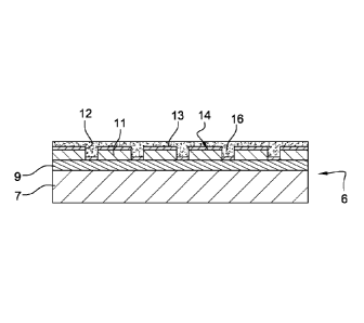
A fifth step, shown in Figure 8, consists in depositing a first active layer
13 on
the top surface 14 of the bodies 11. During the deposition, the first active
layer 13 is also
deposited in the bottom of the recesses 15 formed between the lateral walls
12.
The first active layer 13 is a layer having optical properties, such as an
oxide
layer comprising silicon dioxide. The thickness of the first layer 13 is
approximately
between 90 and 120 nm when working with red fluorescence labels. Any other
dielectric
material, such as a nitride, or a metal layer, could also be used.
Different types of oxide deposition methods can be used such as PECVD
(Plasma-enhanced chemical vapor deposition), evaporation, or sputtering (Madou
MJ,
2002, Fundamentals of microfabrication, CRC Press). For the deposition of
silicon dioxide
from PECVD technique, a mixture of gases such as dichlorosilane or silane and
oxygen
may be used, typically at pressures from a few hundred milliTorr to a few
Torr. The
deposition of the
CA 2879150 2019-05-15
CA 02879150 2015-01-14
WO 2014/016262 PCT/EP2013/065442
silicon dioxide is performed with a temperature comprised in a range from the
room temperature to 300 C.
A sixth step, shown in Figure 9, consists in applying a polymer layer
16 over the first active layer 13, for example a parylen layer or a layer made
of
5 a material known under the references ProTEK, AZ PC 520D or SX AR-PC
5000/40, respectively provided by the companies Brewer Science,
Microchemical and Allresist. The thickness of said polymer layer 16 may be
between 1pm to 100pm. This polymer layer is for example applied by Chemical
Vapor Deposition (CVD) or by spin coating.A seventh step, shown in Figure 10,
10 consists in etching away the bottom layer 7 and the insulating layer 9.
The etching away of the bottom layer 7 is performed by grinding a
major portion of the bottom layer 7 and etching the rest of the bottom layer 7
by
bath etching consisting in dipping the SOI wafer into a potassium hydroxide
bath. Then, the insulating layer 9 is completely etched away by plasma etching
of CHF3 (fluoroform) or by plasma etching of CF4. The etch rate of the
insulating layer is controlled. In order to produce bi-layered microcarriers,
the
method according to the first embodiment of the invention comprises an eighth
step, shown in Figure 11, which consists in depositing a second active layer
17
onto the bottom surface 18 of the bodies 11 of the microcarriers. The second
active layer 17 has also optical properties, such as an oxide layer comprising
silicon dioxide. The thickness of the second layer 17 is approximately between
90 and 120 nm when working with red fluorescence labels. Any other dielectric
material, such as a nitride, or a metal layercould also be used.
The second active layer 17 may be deposited with the same
method used for the deposition of the first active layer 13.
The polymer layer 16 is then etched away in order to separate and
release the bi-layered microcarriers 19, as shown in Figure 12a, for example
by
oxygen plasma. The etch rate is controlled. The microcarriers 19 obtained by
such method each comprise a body 11 having a first active layer 13 on its top
surface 14 and a second active layer 17 on its bottom surface 18. Each active
layer 13, 17 covers homogeneously and continuously the corresponding
surface 14, 18 of the body 11.
CA 02879150 2015-01-14
WO 2014/016262 PCT/EP2013/065442
11
Figures 13 to 17 illustrate another embodiment of the method
according to the invention.
In this embodiment, the wafer 6 shown in Figure 8 is obtained with
the same five steps.
Then, in a sixth step (Figure 13), a support 21 is covered with a
layer of glue 22. The support 21 is for example a wafer made of silicon,
quartz
or glass and has a thickness about 300 to 700 tm. The glue is for example a
resin referenced WaferBOND HT10.10 or CR200 and provided by the company
Brewer Science. The thickness of the glue layer 22 is about 10 to 100 M, and
is preferably about 50 pm.
In a seventh step, shown in Figure 14, the support 21 is bound to
the wafer 6 through the glue layer 22 which contacts and adheres to the first
active layer 13. Such binding is preferably made by pressing and heating the
wafer 6, the support 21 and the glue layer 22.
In a variant, the glue layer 22 is directly applied on the first active
layer 13 and the support 21 is applied onto the glue layer 22.
An eight step, shown in Figure 15, consists in etching away the
bottom layer 7 and the insulating layer 9. This etching step is similar to the
one
performed in Figure 10.
A second active layer 17 can then be deposited onto the bottom
surface 18 of the bodies 11 of the microcarriers (Figure 16).
Then, the support 21 is separated from the wafer 6 by removing the
glue layer 22. Such removal can be made by heating the glue layer 22 or by
using a solvent. The bi-layered microcarriers 19 are thus separated and
released, as shown in Figure 17.
The support 21 provides enhanced mechanical properties in order
to facilitate the handling of the wafer 6 during the production of the
microcarriers.
As shown in Figure 13, during an assay, the functionalized surface
of each microcarrier 19 will emit a homogeneous fluorescent signal so that the
CA 02879150 2015-01-14
WO 2014/016262 PCT/EP2013/065442
12
above mentioned "shadow effect" is avoided. Thus, the use of such
microcarriers 19 provides precise quantitative information during the assay.
The use of bi-layered microcarriers 19 is useful when it is difficult to
control the orientation of the microcarriers during the analysis.
On the contrary, if the orientation of the microcarriers can be
controlled, only the top surface 14 of the bodies 11 can be covered with an
active layer 13.
To this aim, another embodiment of the method according to the
invention proposes to etch the polymer layer 16 directly after the seventh
step,
shown in Figure 10, or to remove the glue layer 22 (in order to separate the
support 21 from the wafer 6) directly avec the step shown in Figure 15.
In this embodiment, as shown in Figure 12b, microcarriers 20
having only one active layer 13 are released. This embodiment involves a less
complex method, enabling the production of less expensive microcarriers 20.
In each embodiment, the released microcarriers 19, 20 may be kept
in suspension in liquid containers or vessels until use in an assay. Each
microcarrier 19, 20 is preferably shaped in the form of a disk and has a
diameter between 1 and 200 ium, for example 40 gm.
Other embodiments of the invention will be apparent to those
skilled in the art from consideration of the specification and practice of the
invention disclosed herein. It is intended that the specification and example
be
considered as exemplary only, with the true scope and spirit of the invention
being indicated by the following claims.