Note: Descriptions are shown in the official language in which they were submitted.
CA 02879170 2015-01-14
WO 2014/015129
PCT/US2013/051064
1
POLARIZATION DIVERSE WAVELENGTH SELECTIVE
SWITCH
CROSS REFERENCE TO RELATED APPLICATION SECTION
[0001] The
present application claims priority to U.S. Provisional Patent Application
Number 61/673,580, filed on July 19, 2012, entitled "Polarization Diverse
Wavelength
Selective Switch." The entire content of U.S. Provisional Patent Application
Number
61/673,580 is herein incorporated by reference.
FIELD OF THE INVENTION
[0002] The
present invention relates to an optical switching device and in particular to
a
wavelength selective switch (WSS) implementing polarization manipulation
optics. While
some embodiments will be described herein with particular reference to that
application, it
will be appreciated that the invention is not limited to such a field of use,
and is applicable
in broader contexts.
BACKGROUND
[0003] Any
discussion of the background art throughout the specification should in no
way be considered as an admission that such art is widely known or forms part
of
common general knowledge in the field.
[0004] With the
development of more complex optical networks, the capabilities of
optical switching devices are evolving. Switches, such as wavelength selective
switches
(WSS) are incorporating more input and output ports to manage the increased
system
demand. Further, WSS devices can be configured to independently route signals
from two
sources within a single device. In such a configuration, a single WSS device
essentially
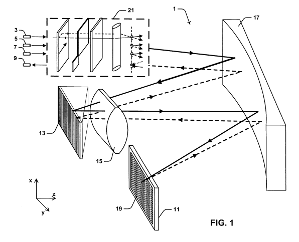
operates as two separate devices. An example of a dual source or "twin" device
is
described in US Patent 7,397,980 to Frisken, entitled "Dual-source optical
wavelength
processor" and assigned to Finisar Corporation.
[0005] However,
constraints on the size of the device generally place limits on the
number and location of possible ports and the functionality of the device.
Further, with
increased port numbers, directivity issues become more prominent as the number
of
possible switching states gives rise to undesired connectivity between pairs
of ports. That
is, establishing a particular link between two ports simultaneously
establishes links
between other pairs of ports. Such undesired links become more common as the
number
CA 02879170 2015-01-14
WO 2014/015129
PCT/US2013/051064
2
of ports in a switching device increases and also as the number of network
switching
points increases, particularly in networks utilizing bidirectional dual source
WSS devices.
Undesired links between ports can establish or enhance multipath interference
in the
beam along the path and can also cause instability in source transmitters such
as lasers.
[0006] In the case of dual source devices, the independent routing of a
dual source
device can be difficult to maintain as the setting up of switching states of a
first optical
source may simultaneously couple signals to ports intended for the second
source. In both
single source and dual source devices, this connectivity issue is often
addressed by
setting up of isolator arrays on the input ports. However, this adds to
optical loss, size and
cost.
[0007] There is a need for improved port isolation in optical switching
devices.
[0008] In current dual source WSS devices beams from the two sources are
propagated separately in space through the optical system. This separation of
beams
requires larger sized optical components and gives rise to increased physical
device size
compared to conventional single source devices. Increase component and device
size
typically leads to increase manufacturing cost.
[0009] There is also a need for improved dual source WSS devices.
SUMMARY OF THE INVENTION
[0010] It is an object of the invention, in its preferred form to provide
an improved or
alternative WSS device.
[0011] In accordance with a first aspect of the present invention there is
provided an
optical switching device for processing optical beams with more than one
independent
wavelength channel, including:
one or more input ports for inputting optical beams in a forward direction of
propagation;
a switching module for reflecting beams propagating in the forward direction
and selectively switching the optical beams along predetermined paths in a
return
direction of propagation;
one or more output ports for receiving predetermined optical beams propagating
in the return direction; and
CA 02879170 2015-01-14
WO 2014/015129
PCT/US2013/051064
3
a port selecting module for selectively directing the beams such that
predetermined ones of the beams propagating in the return direction propagate
along trajectories out of alignment with the input ports.
[0012] The port
selecting module preferably includes one or more polarizing elements
for polarizing the optical beams into a predetermined polarization state. The
port selecting
module preferably further includes:
a polarization separation element for spatially separating an optical beam
into
two orthogonal polarization components; and
a polarization rotation element for selectively rotating the polarization
components with respect to each other.
[0013] The
polarization separation element preferably includes a birefringent walk-off
crystal element.
[0014] The
input and output ports are preferably disposed in an array extending in a
first dimension and the spatial separation of polarization components is in a
second
dimension perpendicular to the first dimension.
[0015] The polarization rotation element preferably includes a Faraday rotator
configured to apply a 45 rotation to a polarization component. The
polarization rotation
element preferably further includes a half-wave plate element configured to
rotate a first
polarization component in a forward propagation direction and to rotate a
second
polarization component in a return propagation direction. The first
polarization component
and the second polarization component are preferably the same component.
[0016] The
optical switching device preferably includes an optical power element for
focusing the polarization components together. The optical switching device
preferably
includes a second polarization separation element for spatially separating the
two
orthogonal polarization components in the first dimension.
[0017] The
polarization rotation element is preferably reconfigurable to allow
selectivity
to define specific ports as being either an input port or an output port. In
one embodiment,
the polarization rotation element preferably includes a transmissive liquid
crystal element
device including a plurality of individually drivable electro-optic cells.
Preferably, the
electro-optic cells are selectively electrically drivable between two discrete
phase states,
one phase state configured to couple an optical beam into a predetermined
output port
and one phase state configured to couple an optical beam away from a
predetermined
output port.
CA 02879170 2015-01-14
WO 2014/015129
PCT/US2013/051064
4
[0018] The
optical switching device preferably includes three input ports and one
output port.
[0019] The
optical switching device preferably includes a dispersive element for
spatially dispersing the optical beams into a plurality of wavelength channels
for
independent selective switching of the channels by the switching module.
[0020] The
optical switching device preferably includes a beam shifting element for
selectively applying a spatial shift to the optical beams in the first
dimension based on the
spatial position and polarization of the beams. In one embodiment, the spatial
shift is
preferably 125 pm.
[0021] In
accordance with a second aspect of the present invention, there is provided
an optical switching method, including:
defining one or more input ports for inputting optical beams in a forward
direction of propagation;
reflecting beams propagating in the forward direction and selectively
switching
the optical beams along predetermined paths in a return direction of
propagation;
defining one or more output ports for receiving predetermined optical beams
propagating in the return direction; and
selectively directing the beams such that beams propagating in the return
direction propagate along trajectories out of alignment with the input ports.
[0022] In
accordance with a third aspect of the present invention, there is provided an
optical signal manipulation system including:
a plurality of ports for carrying a plurality of optical beams to be
manipulated,
each optical beam including a plurality of independent wavelength channels;
a polarizing module for polarizing a first group of beams from the series of
optical beams into a first polarization state and for polarizing a second
group of
beams from the series of optical beams into a second polarization state
orthogonal
to the first state;
a wavelength dispersion element for spatially separating the plurality of
wavelength channels of the first and second groups in the direction of a first
dimension; and
a wavelength manipulation module having:
CA 02879170 2015-01-14
WO 2014/015129
PCT/US2013/051064
a separation element for spatially separating the plurality of wavelength
channels of the first and second groups in the direction of a second
dimension orthogonal to the first dimension; and
a processing device including a series of independent wavelength
processing elements for separately processing each of the separated
wavelengths of the first and second group, with wavelength channels of the
first group being processed independently of wavelength channels of the
second group at a location spatially separated in the second dimension.
[0023] The
optical signal manipulation system preferably includes a beam confining
module for spatially confining the first group of beams with the second group
of beams
along a direction of propagation to a predefined spatial offset in the first
dimension. The
spatial offset in the first dimension is preferably 300 pm. The beam confining
module
preferably includes a polarization beam splitter configured to reflect the
first group of
beams and transmit the second group of beams.
[0024] The beam
confining module preferably includes a pair of spatially offset
substantially parallel reflective surfaces, a first reflective surface of the
pair being
positioned to reflect the first group of beams and a second reflective surface
of the pair
being positioned to reflect the second group of beams. The pair of reflective
surfaces
preferably are both surfaces of a single prism element.
[0025] In one
embodiment, the ports are preferably divided into a first group of ports for
carrying the first group of beams and a second group of ports for carrying the
second
group of beams, and wherein the two groups of ports are disposed parallel to
each other.
In another embodiment, the ports are divided into a first group of ports for
carrying the first
group of beams and a second group of ports for carrying the second group of
beams, and
wherein the two groups of ports are disposed at an angle relative to each
other.
[0026] In
accordance with a fourth aspect of the present invention, there is provided a
wavelength manipulation device for independently manipulating optical beams
from a first
and second source, the optical beams having orthogonal polarizations and
including a
plurality of individual wavelength channels, the device including:
a separation element for spatially separating the optical beams from the first
and second sources by polarization for incidence onto a processing device; and
a processing device including an array of independently controllable
processing
elements for separately and independently processing the beams from the first
and
second sources.
CA 02879170 2015-01-14
WO 2014/015129
PCT/US2013/051064
6
[0027] The
beams are preferably incident substantially normally onto the processing
device. The separating element is preferably configured to receive the beams
in a first
plane and project them onto the processing device in a second plane relative
to the first
plane. The second plane is preferably substantially normal to the first plane.
[0028] The separation element preferably includes a polarization beam splitter
configured to reflect beams from a first source having a first polarization
state and to
transmit beams from a second source having a second polarization state.
[0029] The
wavelength manipulation device preferably includes a reflective element
configured to reflect beams from the second source onto the processing device.
[0030] The
separation element preferably includes a half-wave plate positioned for
rotating the beams of the first source into the same polarization state as the
beams of the
second source.
[0031] The
wavelength manipulation device preferably includes a birefringent wedge
for angularly dispersing the beams from each source prior to incidence onto
the
polarization beam splitter.
[0032] In
accordance with a fifth aspect of the present invention, there is provided an
optical manipulation device, including:
a polarization separation element for spatially separating at least one input
optical
beam into first and second orthogonal polarization components;
a polarization rotation element for rotating the polarization orientation of
the first
polarization component into the same orientation as the second polarization
component;
at least one directing element for directing the first and second polarization
components along substantially parallel but spatially separated output
trajectories.
[0033] The
polarization separation element is preferably a polarization beam splitter.
The polarization rotation element is a preferably reflective half-wave plate.
The reflective
half-wave plate preferably defines, in part, the at least one directing
element for directing
the first polarization component. The at least one directing element
preferably includes an
angled mirror for directing the second polarization component.
[0034] The
optical manipulation device preferably includes a second polarization
separation element for angularly separating the at least one input beam into
orthogonal
polarization components. The second polarization separation element is
preferably a
birefringent wedge. The second polarization separation element preferably
angularly
CA 02879170 2015-01-14
WO 2014/015129
PCT/US2013/051064
7
separates the orthogonal polarization components in a dimension perpendicular
to the
spatial separation performed by the first polarization separation element.
[0035] The output trajectories of the polarization components are preferably
substantially perpendicular to the trajectory of the at least one input
optical beam.
[0036] The
optical manipulation element preferably includes a processing device
having an array of independently controllable processing elements for
separately and
independently processing the first and second polarization components.
[0037] In
accordance with a sixth aspect of the present invention, there is provided a
wavelength manipulation device for independently manipulating optical beams
from a first
and second source, the optical beams having orthogonal polarizations and
including a
plurality of individual wavelength channels, the device including:
an electrically controllable directing element for simultaneously selectively
spatially
directing the optical beams from both the first and second sources along
predefined
trajectories onto a processing device; and
a processing device including an array of independently controllable
processing
elements for separately and independently processing the beams from the first
and
second sources.
[0038] The
electrically controllable directing element preferably includes a MEMS
mirror. In one embodiment, the electrically controllable directing element is
preferably
configured to vary the predefined trajectories in response to data indicative
of a local
temperature of the device. In another embodiment, the electrically
controllable directing
element is preferably responsive to a detected optical reference signal.
[0039] In
accordance with a seventh aspect of the present invention, there is provided
an optical manipulation method, including:
receiving one or more polarized optical beams at a position along a first axis
perpendicular to a propagation direction of the one or more beams;
applying a spatial shift to the one or more beams along the first axis based
on the
polarization and position of the one or more beams along the first axis; and
simultaneously compensating the one or more beams for one or more aberrations
based on the position of the one or more beams along the first axis.
CA 02879170 2015-01-14
WO 2014/015129
PCT/US2013/051064
8
BRIEF DESCRIPTION OF THE DRAWINGS
[0040]
Preferred embodiments of the disclosure will now be described, by way of
example only, with reference to the accompanying drawings in which:
Fig. 1 is a schematic perspective view of a WSS device according to a first
embodiment;
Fig. 2 is a schematic exploded perspective view of a port selecting module for
an
optical switch, showing polarization states of optical beams throughout the
module;
Fig. 3 is a schematic illustration of a symmetric polarization loop
established in the
WSS of Fig. 1;
Fig. 4 is a schematic plan view of the selecting module of Fig. 2 showing the
trajectory and polarization states of an optical beam passing through the
module
between an input port and an output port;
Fig. 5 is a schematic plan view of the selecting module of Fig. 2 showing the
trajectory and polarization states of an optical beam passing through the
module
between two input ports;
Fig. 6 is a schematic perspective view of a half-wave plate in the form of a
reconfigurable transmissive liquid crystal device;
Fig. 7 is a schematic illustration of a symmetric polarization loop
established in the
WSS of Fig. 1, showing diffractive effects at the LCOS device;
Fig. 8 is a schematic exploded perspective view of a port selecting module for
an
optical switch according to a second embodiment, showing polarization states
of
optical beams throughout the module;
Fig. 9 is a plan view of a beam shifting element used in the port selecting
module
of Fig. 8, illustrating beam components in the input direction;
Fig. 10 is a plan view of a beam shifting element used in the port selecting
module
of Fig. 8, illustrating 'wanted' beam components in the return direction;
Fig. 11 is a plan view of a beam shifting element used in the port selecting
module
of Fig. 8, illustrating 'unwanted' beam components in the return direction;
CA 02879170 2015-01-14
WO 2014/015129
PCT/US2013/051064
9
Fig. 12 is a schematic perspective view of a WSS device according to a second
embodiment;
Fig. 13 is a sectional front view of an LCOS device showing the relative
positioning
of wavelength channels between two input sources;
Fig. 14 is a schematic plan view of a beam confining module according to an
embodiment;
Fig. 15 is a schematic plan view of a beam confining module according to
another
embodiment;
Fig. 16 is a side view of a separation element used in the WSS device of Fig.
12;
Fig. 17 is a schematic illustration of a WSS device incorporating a beam
correction
module with electrically controllable MEMS mirror for providing simultaneous
active beam control to two independent optical devices;
Fig. 18 is schematic plan view of the beam correction module used in the WSS
device of Fig. 17;
Fig. 19 is a sectional side view of an alternate beam correction module
wherein the
MEMS mirror is mounted co-planar with the substrate;
Fig. 20 is a plan view of a turning mirror used in an embodiment of the beam
correction module; and
Fig. 21 is a schematic illustration of the evolution of the polarization state
of the
beam through a turning mirror and a quarter-wave plate.
DETAILED DESCRIPTION
[0041] The
techniques and improvements included in the present application will be
described in the context of an optical wavelength selective switch (WSS) for
switching
wavelength channels contained within wavelength division multiplexed (WDM)
optical
signals. For example, the optical signals may comprise dense wavelength
division
multiplexed signals including a plurality of individual wavelength channels
equally
spectrally separated by 50 GHz. However, it will be appreciated that these
techniques and
improvements are able to be implemented in other types of optical switching
and
manipulation devices.
CA 02879170 2015-01-14
WO 2014/015129
PCT/US2013/051064
GENERAL OPERATION OF THE WSS OPTICAL SWITCH
[0042]
Referring initially to Fig. 1, there is illustrated an exemplary WSS optical
switching device 1 configured for switching input optical beams from three
input optical
fiber ports 3, 5 and 7 to an output optical fiber port 9. Ports 3, 5, 7 and 9
are adapted for
releasable connection to respective optical fibers (not shown). The optical
beams are
indicative of WDM optical signals, as mentioned above. On a broad functional
level,
device 1 performs a similar switching function to that described in US Patent
7,397,980 to
Frisken, entitled "Dual-source optical wavelength processor" and assigned to
Finisar
Corporation, the contents of which are incorporated herein by way of cross-
reference. The
optical beams propagate from input ports 3, 5 and 7 in a forward direction and
are
reflected from a liquid crystal on silicon (LCOS) device 11 (described below)
in a return
direction to output port 9.
[0043] Ports 3,
5, 7 and 9 are equally spaced apart along a first axis (x-axis) by a
distance of about 250 pm so as to accommodate optical fibers disposed in a
fiber v-
groove array, which are also equally spaced by 250 pm. In other embodiments,
ports 3, 5, 7 and 9 are equally spaced apart in the x-axis by other distances.
In further
embodiments, ports 3, 5, 7 and 9 are not equally spaced apart in the x-axis.
In some
embodiments, ports 3, 5 and 7 include micro-lenses for controlling the
divergence and
profile of the beams exiting or entering the ports from connected optical
fibers. In one
embodiment, these micro-lenses are mounted to the optical fibers themselves.
In another
embodiment, the micro-lenses are disposed in an array adjacent the ports in
the z-axis or
propagation direction. In a further embodiment, micro-lenses are included in a
fiber v-
groove array disposed along the x-axis.
[0044] Device 1
includes a wavelength dispersive grism element 13 for spatially
dispersing the individual wavelength channels from an input optical beam in
the direction
of a second axis (y-axis). Grism element 13 operates in similar a manner to
that described
in US Patent 7,397,980. That is, to spatially separate the constituent
wavelength channels
contained within each optical beam in the y-axis according to wavelength. In
various
embodiments, grism 13 may be formed of suitable materials to provide a low
polarization
dependent loss or a reduced polarization sensitivity to further enhance the
polarization
diversity of device 1.
[0045] A
collimating lens 15 is positioned adjacent to grism 13 such that the optical
beams traverse the lens both prior to incidence onto grism 13 and after
reflection from the
grism. This double pass of lens 15 acts to collimate beams in the x-axis.
Similarly, in
propagating between input ports 3, 5 and 7 and LCOS device 11, the beams
reflect twice
CA 02879170 2015-01-14
WO 2014/015129
PCT/US2013/051064
11
off a cylindrical mirror 17. Mirror 17 has appropriate curvature in the y-axis
such that each
dispersed channel is focused in the y-axis onto the LCOS device. In another
embodiment
(not shown), focusing in the y-axis is provided by two cylindrical mirrors,
each having
substantially the same radius of curvature in the y-axis. In further
embodiments, the
cylindrical mirrors have different radii of curvature.
[0046] The
dispersed wavelength channels are incident onto LCOS device 11, which
acts as a reflective optical manipulation device to independently steer each
channel in the
x-axis. At the device level, LCOS device 11 operates in a similar manner to
that described
in US Patent 7,092,599 to Frisken, entitled "Wavelength manipulation system
and
method" and assigned to Finisar Corporation, the contents of which are
incorporated
herein by way of cross-reference. However, due to the flexibility available in
these
devices, LCOS device 11 is also able to be driven in other arrangements, such
as in a
dual source mode of operation, as described below.
[0047] LCOS
device 11 includes a two-dimensional array of substantially square-
shaped cells 19 formed in a layer of liquid crystal material. In an exemplary
embodiment,
device 11 includes an array of 1280 by 768 cells. Each cell is independently
electrically
drivable to impose a relative phase shift to a local region of an incident
optical beam. The
cells are able to be driven at different relative levels to define a phase
profile which
manipulates the optical wavefront to selectively steer the beam.
[0048] LCOS
device 11 steers the wavelength channels at certain angles along
predetermined paths in a return direction such that some wavelengths are
coupled to
output port 9. Other wavelength channels are steered at other angles that
couple them
away from output port 9, thereby dropping them from the system.
[0049] It will
be appreciated that in other embodiments, device 1 includes different
numbers of input and output ports and is configured to simultaneously couple
beams
between different input and output ports. In some embodiments, grism 13 is
replaced with
a diffraction grating or other diffractive device. In some embodiments, LCOS
device 11 is
replaced with a micro-electromechanical mirror (MEMS) based optical
manipulation
device or other type of optical manipulation device.
[0050]
Referring still to Fig. 1, the input optical beams are transmitted through a
port
selecting module 21, which provides polarization diversity to device 1 and
provides
capability to restrict optical beams returning from LCOS device 11 from being
coupled
back into input ports 3, 5 and 7. The operation of port selecting module 21 is
described
below.
CA 02879170 2015-01-14
WO 2014/015129
PCT/US2013/051064
12
PORT SELECTIVITY IN THE WSS
[0051]
Referring to Fig. 2, there is illustrated a schematic exploded side view of
port
selecting module 21. In traversing module 21, example optical beam 22
initially passes
through a polarization separation element in the form of a birefringent walk-
off crystal
element 23 for spatially separating in the y-axis an optical beam into two
orthogonal
polarization components. A first polarization component 25 of each optical
beam is
designated by solid circles. A second polarization component 27 of each
optical beam is
designated by dashed circles. The illustrated orientations of the polarization
states is
exemplary only and it will be appreciated by the skilled person that arbitrary
orthogonally
polarization states can be generated.
[0052] Walk-off
element 23 is formed of a birefringent crystalline material that has a
material optic axis disposed at an angle relative to the surface normal. Beam
components
polarized parallel to the crystalline optic axis (parallel to component 27 in
the illustrated
embodiment) are refracted or walked-off from the original direction of
propagation by an
amount dependent on the refractive index and thickness of the element. Beam
components polarized perpendicular to the crystalline optic axis are
unaffected by the
material. In preferred embodiments, walk-off element 23 has a thickness in the
order of
millimeters and provides a spatial separation of polarization components in
the order of
microns. In the illustrated embodiment, the beams are separated into
components having
vertical and horizontal orientations and propagating parallel at the output of
element 23.
However, in other embodiments, element 23 is able to be configured to split
the beams
into pairs of orthogonal polarization components having any orientation.
[0053] In
another embodiment, walk-off element 23 is replaced with a birefringent
wedge, which angularly separates two orthogonal components by an angle
determined by
the refractive index and angle of the wedge. In embodiments incorporating
birefringent
wedges, it is sometimes necessary to angle input ports with respect to output
ports or
vise-versa in the direction of polarization separation (y-axis).
[0054] The beam
components output from walk-off element 23 are then passed
through a half-wave plate element 29. This element includes birefringent
regions 31
and 33 which impose a 180 or 7 radians phase shift between constituent sub-
components of that particular polarization component to rotate the
polarization by 90 .
Region 31 of element 29 is configured to rotate component 27 propagating in
the forward
direction by 90 . Component 25 is passed through element 29 without rotation.
After
passing through element 29, both components propagate in the vertical
orientation, as
CA 02879170 2015-01-14
WO 2014/015129
PCT/US2013/051064
13
illustrated in Fig. 2. Exemplary birefringent materials that are used to form
regions 31
and 33 include calcite, tourmaline, quartz, sodium nitrate, lithium niobate
and rutile.
[0055] Region
33 of element 29 is configured to rotate component 27 again in the
return direction by 90 . However, it will be appreciated that, in other
embodiments, the
location of regions 31 and 33 can be varied in the y-axis to rotate the other
polarization
components of each beam. These other embodiments are able to provide the same
functionality as that illustrated in Fig. 2. The general requirement is that
the location of
regions 31 and 33 must be oppositely disposed in the y-axis about the vertical
center (x-
axis) of element 29 such that the same components rotated in the forward
direction are
again rotated in the return direction. That is, region 31 may be disposed to
the left of
region 33 in the y-axis or, alternatively, region 31 may be disposed to the
right of
region 33 in the y-axis.
[0056] The
specific location of regions in the x-axis defines which ports will operate as
input ports and which ports will operate as output ports. By way of example,
in Fig. 2,
beams from the input ports 3, 5 and 7 are transmitted through region 31 of
element 29
and beams returned to output port 9 are transmitted through region 33, which
is disposed
opposite to region 31 in the y-axis.
[0057] It will
be appreciated that in other embodiments, the location of regions 31
and 33 differ and define devices having different arrangements of input and
output ports.
Further, as will be described below, in one embodiment, element 29 is
reconfigurable to
define different positions for regions 31 and 33 for beams between different
arrangements
of input and output ports.
[0058] In one
embodiment, element 29 is at least partially formed from a non-
birefringent and substantially transparent substrate on which birefringent
materials are
mounted to define birefringent regions such as regions 31 and 33. In some
embodiments,
the birefringent materials are able to be moved and mounted or adhered to
different
locations of the substrate to provide flexibility to reconfigure which ports
in device 1 are to
operate as input ports and which ports are to operate as output ports. In one
particular
embodiment, the substrate is formed of glass. In another embodiment, regions
31 and 33
define separate half-wave plate elements, which are able to be positioned at
relative
positions along the optical z-axis in alignment with the corresponding beam
components.
[0059] At the
output of element 29 in the forward propagation direction, components 25
and 27 have a common vertical orientation . The components 25 and 27 are then
passed
through a Faraday rotator 35 configured to apply a 45 rotation to each
polarization
CA 02879170 2015-01-14
WO 2014/015129
PCT/US2013/051064
14
component 25 and 27. Rotator 35 is a non-reciprocal element which applies the
same
polarization rotation to beams independent of propagation direction through
the element.
As such, in the reverse direction of propagation, rotator 35 again applies a
45 rotation to
each component 25 and 27, as illustrated in Fig. 2. In the illustrated
embodiment, at the
output of the rotator 35 in the forward direction, each polarization component
25 and 27
has a +45 orientation. In other embodiments, the polarization components 25
and 27
have other orientations, depending on the particular configuration of optical
separation
and rotation elements.
[0060] In many
cases the optical isolation that is achieved in this operation can be
advantageous though in some cases this will impose a limitation. If a single
polarization is
imposed to a beam (either intentionally or because of single polarization
operation of any
component) then the wavelength switch function will be nonreciprocal
(isolating) however
if no polarizing element is imposed within the switching train then the
overall device
function will remain reciprocal. In some embodiments, isolation is established
between
forward and return path through a spatial offset. An exemplary embodiment
utilizing this
isolation is described below in relation to Fig. 8. Another embodiment
providing improved
isolation involves establishing a retro reflection point at the switching
matrix. In these
embodiments, spatial diversity is able to be used to achieve the enhanced
directivity
rather than polarization isolation.
[0061] After
propagation through Faraday rotator 35 in the forward direction, the
polarization components are passed through a cylindrical lens 37 having
optical power in
the y-axis. Lens 37 angularly converges the polarization components together
at focal
plane 39, which defines a first point of symmetry in device 1 of Fig. 1.
Referring again to
Fig. 1, the polarization components propagate through device 1 separately and
are
recombined at the LCOS device 11, which defines a second point of symmetry in
device 1. Between plane 39 and LCOS device 11, a symmetric polarization loop
is
established, as illustrated schematically in Fig. 3.
[0062]
Referring to Fig. 3, along the loop, one polarization component propagates
clockwise, while the orthogonal component propagates anti-clockwise. Module 21
rotates
both polarization components into a common orientation (vertical in the
illustrated
embodiment) such that polarization dependent effects in the system are
equalized. At
focal plane 39, these two polarization components are spatially confined, as
shown in Fig.
3. At the LCOS device 11, both components are again confined so that they can
be
simultaneously manipulated by common cells of device 11. In other embodiments,
the
polarization components are rotated into orientations other than vertical. As
the LCOS
CA 02879170 2015-01-14
WO 2014/015129
PCT/US2013/051064
device is polarization dependent, the polarization components are preferably
rotated into
alignment with the polarization axis of the LCOS device. In other embodiments
utilizing
spatial light modulators other than LCOS devices, this alignment of the
polarization
components with a predefined axis may not be required.
[0063] In other
embodiments, module 21 is placed at other locations in the optical
system and performs substantially the same function as described above. The
general
requirement is that the polarization equalization performed by module 21
occurs before
the optical beams reach polarization dependent optical elements such grism 13
and
LCOS 11 of Fig. 1.
[0064] When the
polarization components return to port selecting module 21 of Fig. 2,
they converge at plane 39 and are collimated in passing back through lens 37.
The
components return through Faraday rotator 35, half-wave plate element 29 and
walk-off
element 23 in a similar manner to that described in relation to the forward
direction. Walk-
off element 23 either recombines the components for coupling to output port 9
or couples
them out of alignment with the ports to attenuate them. The selection of which
beam to
couple to the output port is made by the LCOS device, which is selectively
driven to apply
a predetermined switching angle to the beams in the x-axis. In conventional
WSS devices,
the establishment of a particular switching state from one input port to an
output port
simultaneously couples beams between other ports that are symmetric about that
switching angle. By way of example, in device 1 illustrated in Fig. 1,
switching a beam
from input port 3 to output port 9 will simultaneously switch beams from input
port 5 to
input port 7, potentially giving rise to multipath interference in signals
transmitted between
ports 5 and 7 and instabilities in laser sources connected to those ports.
[0065] The
particular configuration of elements in port selecting module 21 acts to
reduce or minimize this undesired cross coupling between input ports through a
selective
process of coupling polarization states. This process will now be described
with reference
to Figs 4 and 5, which illustrate schematic plan views of port selecting
module 21 of Fig. 2.
Referring initially to Fig. 4, there is illustrated a schematic plan view of
port selecting
module 21 illustrating the spatial evolution of beams propagating between
input port 3 and
output port 9. As in Fig. 2, first polarization component 25 is indicated by
solid circles and
the orthogonal component 27 is indicated by dashed circles.
[0066] As
described above, in the forward direction, input port 3 projects optical
beam 22 through walk-off element 23, half-wave plate element 29 and Faraday
rotator 35
to spatially separate the two orthogonal polarization components and rotate
them into the
same orientation. In this forward direction, component 25 remains aligned with
input port 3
CA 02879170 2015-01-14
WO 2014/015129
PCT/US2013/051064
16
in the y-axis and component 27 is refracted out of alignment with port 3 by
walk-off
element 23.
[0067] In the
return direction, component 27 is axially aligned with output port 9 and
component 25 is out of alignment with output port 9. In this return direction,
both
components pass through rotator 35 and are rotated 45 such that they are both
oriented
horizontally. Second component 27 is passed through birefringent region 33 to
rotate it
into a vertical orientation. Component 25 passes through element 29 without a
rotation in
orientation and reaches walk-off element 23 in a horizontal orientation and
offset from
output port 9. In traversing walk-off element 23, component 25 experiences
walk-off and is
refracted towards port 9 due to its alignment with the preferred axis of
element 23 (
horizontal in this embodiment). After passing walk-off element 23, component
25 is axially
aligned with port 9 in the y-axis. Component 27 is in the vertical orientation
and passes
directly through walk-off element 23 without refraction, thereby remaining
axially aligned
with output port 9. Therefore, both components 25 and 27 are recombined and
coupled
efficiently into output port 9. Similar coupling occurs between ports 5 and 9,
and between
ports 7 and 9 and the optical loss incurred by each polarization state is
substantially
equal.
[0068] Due to
symmetry in the optical system, to perform the switching described
above, LCOS device 11 also simultaneously sets up a switching path between
input
ports 5 and 7 of Fig. 2. Referring now to Fig. 5, there is illustrated a
schematic plan view
of port selecting module 21 illustrating the spatial evolution of beams
propagating between
input port 5 and input port 7. As with Figs 2 and 4, polarization component 25
is indicated
by solid circles and the orthogonal component 27 is indicated by dashed
circles.
[0069]
Propagation in the forward direction from port 5 is identical to that
described
above in relation to Fig. 4. However, in the return direction, the system is
asymmetric due
to the positioning of region 31 of element 29. Component 25 passes through
region 31 of
element 29, experiencing a polarization rotation of 90 into a vertical
orientation.
Component 27 is unaffected by element 29 and remains in a horizontal
orientation. In
passing through walk-off element 23, component 27 experiences walk-off due to
its
polarization alignment with the preferred axis of the element. This walk-off
refracts
component 27 out of alignment with input port 7. Component 25 is not affected
by
element 23 due to its anti-alignment with the preferred axis of element 23.
Component 25
passes directly through element 23 and remains out of alignment with input
port 7.
Therefore, neither component is coupled to input port 7.
CA 02879170 2015-01-14
WO 2014/015129
PCT/US2013/051064
17
[0070]
Comparing Figs 4 and 5, it can be seen that the symmetry in optical path
between input port 3 and output port 9 provides effective coupling of an
optical beam
between the ports. However, the asymmetry in optical path between input port 5
and input
port 7 restricts the optical beam from coupling between the input ports,
significantly
reducing interference effects to optical signals from the other input ports.
The symmetry is
controlled by the relative positioning of the half-wave plate regions 31 and
33 such that
both separated polarization components undergo the same relative changes in
the return
direction as in the forward direction. This symmetry is not present between
two input
ports, only between input ports and output port 9.
[0071] As
illustrated in the plan views of Figs 4 and 5, switching paths that include a
half-wave plate element on opposite sides (in the y-axis) between the forward
and return
directions will provide symmetry and therefore facilitate coupling between an
input port
and output port. Conversely, switching paths that include a half-wave plate
element on the
same side (in the y-axis) between the forward and return directions will not
provide
symmetry and therefore will not couple beams between the fibers. A symmetric
path
defines a switching path and an asymmetric path defines a non-switching path.
From this
it can be observed that the choice of a switching path can be made by the
relative
positioning of half-wave plate elements in the y-axis.
[0072]
Referring generally to Figs 2 to 5, it will be appreciated that the
orientations of
the particular polarization components described above are exemplary only. In
other
embodiments, module 21 is configured to manipulate polarization components
having
different orientations while performing the same functionality. Specifically,
walk-off
element 23 is configured to split optical beams into polarization components
other than
horizontal and vertical. Similarly, the relative position of regions 31 and 33
of element 29
are able to be interchanged while still performing the same overall
polarization
manipulation.
[0073] In
another embodiment (not shown), module 21 includes a half-wave plate
located between element 29 and lens 37. This additional half-wave plate is
configured to
apply a further arbitrary polarization rotation so as to propagate the beams
through
device 1 in a preferred polarization state. In a further embodiment, element
29 includes an
array of half-wave plates that act to apply different rotations to each of the
beams so that
they can arrive at the Faraday rotator at an equal but arbitrary orientation.
[0074] In one
embodiment (not shown) module 21 includes an additional polarizing
element having a polarizing axis oriented along a preferred axis. In one
embodiment this
polarizing element is located between elements 35 and 37. The polarizing
element acts to
CA 02879170 2015-01-14
WO 2014/015129
PCT/US2013/051064
18
filter out optical power that has strayed from the desired orientation so as
to improve
isolation between polarization states.
[0075]
Referring now to Fig. 6, there is illustrated an alternative embodiment half-
wave
plate element in the form of a reconfigurable transmissive liquid crystal
device 41.
Device 41 is able to replace element 29 of Figs 2, 4 and 5. Like LCOS device
11 of Fig. 1,
device 41 includes a two-dimensional array of independently drivable phase
manipulating
cells configured to impose a relative phase shift to a local area of an
incident optical
beam. The cells are divided into eight regions 43, 45, 47, 49, 51, 53, 55 and
57 that are
axially aligned with polarization components of each beam (walk-off element 23
is omitted
from Fig. 6 for simplicity). Within each region, the cells are selectively
electrically driven at
one of two discrete polarization rotation states. A first state (illustrated
by the vertical lines
across regions 45, 47, 51 and 55) imposes a relative phase change of 180 or 7
radians
phase shift between constituent sub-components of that particular polarization
component
to rotate the polarization by 90 . That is, regions driven in the first state
operate as a half-
wave plate. A second state imposes little or no phase change to essentially
pass the
polarization component without rotation.
[0076] This
selective driving in one of two states allows selectively defining of specific
ports as being configured as either an input port or an output port.
Specifically, defining a
symmetric switching path between two ports allows coupling from one port to
the other. By
way of example, device 41 includes four vertically separated pairs of
horizontally adjacent
cells. In the top pair of regions, region 45 is driven in the first state and
region 43 is driven
in a second state. The adjacent three pairs of regions below are driven with
an opposite
configuration. This sets up symmetric switching paths between port 3 and any
one of
ports 5, 7 and 9. Therefore, in one configuration, port 3 can be used as an
input port and
ports 5, 7 and 9 as output ports. Alternatively, ports 5, 7 and 9 can be used
as input ports
while port 3 is used as an output port.
[0077] In WSS
devices implementing pixilated spatial light modulators, such as LCOS
and MEMS (for example, Texas Instruments DLPTM) devices, undesired diffraction
effects
are experienced due to the inherent periodic pattern of the cell structure.
The periodicity of
the LCOS surface results in a small amount of uncontrolled diffraction in
addition to the
steering applied to each beam. Referring now to Fig. 7, the symmetric loop
path of Fig. 3
is shown with the addition of extra diffraction effects originating from LCOS
device 11,
illustrated as dashed arrows at the LCOS device. While most of the light is
directed along
the steering paths 59 and 61, some light is diffracted along other paths, e.g.
path 63. If
one of these paths is aligned with the input path, then a particular
polarization component
CA 02879170 2015-01-14
WO 2014/015129
PCT/US2013/051064
19
will be coupled back to the originating input port, resulting in undesired
interference effects
which degrade the overall device performance.
[0078] Standard
polarization diversity schemes do not compensate for these diffractive
coupling effects. Referring now to Fig. 8, there is illustrated another
embodiment port
selecting module 65 which is capable of compensating for the above described
diffractive
coupling effects. Corresponding features of module 21 are designated by the
same
reference numerals in module 65. Module 65 includes a beam shifting element 67
located
between walk-off crystal 23 and half-wave plate element 29. Module 65 is
comprised of a
pair of birefringent wedges, configured to shift one polarization component
with respect to
the other in the x-axis. This shift can be seen more clearly in Fig. 9.
[0079] Turning
to Fig. 9, there is illustrated a plan view of beam shifting element 67
showing propagation of optical beam 22 therethrough. Beam 22 is initially
incident onto
birefringent wedge 71, which has a crystalline optic axis oriented such that
it refracts or
'walks off' component 25 (having a vertical polarization orientation) downward
in the x-
axis. Birefringent wedge 71 is configured such that component 27 (having a
horizontal
polarization orientation) passes without any change. The components then
propagate
through a second birefringent wedge 73, which has a crystalline optic axis
oriented
orthogonal to that of wedge 71. In propagating through wedge 73, component 25
is
walked off upward in the x-axis. The width of wedge 73 is greater than that of
wedge 71
and so component 25 experiences a net refraction upward from its original
trajectory in
the x-axis. Through wedge 73, component 27 again remains unrefracted. The
choice of
wedge angle here is appropriate to compensate for 1st order effects of the
polarization
dependent switching displacement and may be chosen to optimize any optical
design
involving polarization diversity and multiple ports.
[0080] In
effect, element 67 acts to both shift the beams to apply a 125 pm (or other)
beam displacement, and also to apply correction to beams that are offset from
the desired
propagation path. As shown in Fig. 9, the beam shifting function is performed
by the right
had side of wedge 73 and the beam correction is performed by the combination
of the left
hand side of wedge 73 and wedge 71. In the beam correction section of the
element 67,
wedges 71 and 73 have different thicknesses as a function of 'x' position.
This means that
polarization components that travel at different heights 'x' in device 1 will
exit the beam
correction section with a small 'x' offset. This subtle variation in the
offset as a function of
'x' compensates for system aberrations, and substantially reduces the overall
polarization
dependent loss in device 1.
CA 02879170 2015-01-14
WO 2014/015129
PCT/US2013/051064
[0081] It will
be appreciated that, in other embodiments, different methods of shifting
one polarization component with respect to the other. In one exemplary
embodiment,
element 67 consists only of the right hand beam shifting side of wedge 73. In
another
exemplary embodiment, element 67 includes a beam compensator that refracts one
polarization state at an angle such that, at the output, it is displaced by
about 125 pm from
the other polarization component.
[0082] At the
output of element 67, the two components propagate parallel but with
a 125 im separation in the x-axis, which is half the spacing of the input and
output ports.
Referring again to Figs 7 and 8, the system is symmetric such that components
that
propagate along the steering paths 59 and 61 are recombined by element 67 and
coupled
to the corresponding output port. That is, component 25, which was shifted by
element 67
in the forward direction, is shifted back to its original position in the x-
axis in the reverse
direction. Consequently, components 25 and 27 trace the same paths back
through
element 67 on the return path and are coupled to an output port.
[0083]
Conversely, components that are diffracted by the LCOS device and coupled
back along the input path will not be coupled to an output port. These
components
propagate back through module 65 where Faraday rotator 35 and half-wave plate
element 29 rotate the polarization components into the orthogonal orientation
to that of the
forward direction. Then, upon reaching beam shifting element 67, the component
not
shifted in the forward direction (component 27 in the illustrated embodiment)
is shifted in
the return direction. Similarly, the component shifted in the forward
direction
(component 25 in the illustrated embodiment) is not shifted in the return
direction. This
situation is illustrated in Fig. 10, which illustrates a plan view of beam
shifting element 67
showing propagation of 'unwanted' components of beams 25 and 27 in the return
direction
to exemplary output port 9. Here, the position of each component 25 and 27 is
reversed
from that of Fig. 9. This situation results in both components being shifted
and offset by
125 im out of alignment with output port 9, thereby restricting the components
from
coupling back to port 9. The situation of 'wanted light' is illustrated in
Fig. 11 wherein the
components of beams 25 and 27 that are coupled correctly and symmetrically are
returned in axial alignment with output port 9.
[0084]
Therefore, port selecting module 65 restricts back coupling of optical beams
from LCOS device 11, thereby reducing interference effects and improving
device
performance.
[0085] The
particular shift spacing of 125 Rm is chosen as the input and output fibers
are disposed in an array having a fiber spacing of 250 tim. Therefore, a shift
of 125 im
CA 02879170 2015-01-14
WO 2014/015129
PCT/US2013/051064
21
centres the beams directly between two adjacent ports to minimise cross-
coupling
between the ports. In other embodiments utilizing different fiber port
spacings, element 65
is configured to provide different shifts in the x-axis to accommodate the
different spacing
of the ports. In further embodiments element 67 is replaced with a walk-off
crystal which
provides an equivalent 125 jim offset in the x-axis.
[0086]
Therefore, the above embodiments provide efficient switching of optical beams
in a WSS device independent of polarization. Beams being switched between an
input
port and an output port are coupled efficiently while inadvertent switching of
beams
between two input ports is significantly reduced.
DUAL SOURCE ARCHITECTURE
[0087] As
mentioned above, WSS devices can also be configured to operate as dual
source devices wherein two groups of optical beams are independently coupled
between
two sources sharing a common optical system. In known dual source WSS devices,
beams from each source are typically separated in angle and/or space in
propagation
through the device to differentiate the two sources. The angular separation
can give rise
to aberrations due to angular incidence onto the diffractive grism and LCOS
device. The
spatial separation requires a larger optical setup with larger components,
leading to
increased cost.
[0088]
Referring now to Fig. 12 there is illustrated a further embodiment WSS
device 75 configured to operate as a dual source device. Device 75 is
constructed to
reduce these spatial and angular separation requirements that are present in
conventional
dual source WSS devices. Corresponding features of earlier described
embodiments are
indicated by the same reference numerals.
[0089] Device
75 includes a plurality of ports, which are divided into a first group 77 for
carrying a first group of beams corresponding to a first optical device
(Source A) and a
second group of ports 79 for carrying a second group of beams corresponding to
a
second optical device (Source B). Source A is configured to switch an optical
beam 81
from input port 83 to one or more of a first set of twenty three output ports
85 and 87 (only
two are shown for simplicity). Simultaneously and independently, Source B is
configured
to switch an optical beam 89 from input port 91 to one or more of a second set
of twenty
three output ports 93 and 95 (again, only two are shown for simplicity). In
other
embodiments, different numbers of output ports are included in each device.
[0090] The two
groups of ports 77 and 79 are disposed parallel to each other and
transmit beams through corresponding independent polarizing port selecting
modules 97
CA 02879170 2015-01-14
WO 2014/015129
PCT/US2013/051064
22
and 99. In addition to providing appropriate polarization manipulation,
modules 97 and 99
are configured to output beams 81 and 89 in orthogonal polarization states. In
the
illustrated embodiment, module 97 outputs a beam with vertical polarization
and
module 99 outputs a beam with horizontal polarization. In one embodiment,
modules 97
and 99 comprise port selecting module 21 of Fig. 2, with one module including
elements
oriented to provide vertical beam output and the other module including
elements oriented
to provide horizontal beam output. In some embodiments, modules 97 and 99
include port
selecting module 21 of Fig. 2 in addition to other optics. In one embodiment,
modules 97
and 99 include only polarizers oriented with their axes aligned to output the
required
polarization orientation. In further embodiments, other known polarization
diversity
systems are implemented in place of, or in addition to modules 97 and 99.
[0091]
Referring still to Fig. 12, beams 81 and 89 are passed through a beam
confining
module 101 for spatially confining and realigning beams 81 and 89 along a
direction of
propagation (z-axis). This spatial confinement reduces the necessary size of
the optical
system and associated coupling elements, and allows for more efficient use of
space on
LCOS device 11. At the same time, the beams are restricted from being
spatially
overlapped so as to maintain isolation between the signals from the two
sources. In one
embodiment, beams 81 and 89 are confined to a spatial offset of about 300 pm
in the y-
axis (wavelength dispersion axis). In other embodiments, the offsets are
chosen by the
beam size in the system, and the required optical isolation between sources A
and B.
[0092] The
spatial offset defined by module 101 emerges as an offset of individual
wavelength channels at LCOS device 11. Referring now to Fig. 13, there is
illustrated
schematically front view of a region of LCOS device 11. As shown, the offset
of 300 pm
defined by confining module 101 provides a 300 pm offset between corresponding
wavelength channels of sources A and B in the y-axis. This offset provides
enhanced
isolation between signals from sources A and B.
[0093]
Returning to Fig. 12, confining module 101 includes an angled mirror 103,
which
reflects beam 81 and directs it perpendicularly towards beam 89. Both beams
are passed
through a polarization beam splitter (PBS) 105 that is configured to reflect
beam 81.
Beam 89, having an orthogonal polarization orientation, is not affected by the
reflective
surface and passes directly through PBS 105. At the output of module 101,
beams 81
and 89 propagate parallel with a predefined spacing.
[0094] It will
be appreciated that fiber arrays 77 and 79 corresponding to sources A
and B need not be disposed parallel to each other. By suitable angling of
mirror 103, the
two sources are able to be angled with respect to each other. In one exemplary
CA 02879170 2015-01-14
WO 2014/015129
PCT/US2013/051064
23
embodiment, fiber array 77 from Source A is disposed perpendicularly to fiber
array 79 of
Source B. This arrangement of fibers provides simplicity for aligning the
beams and
enhanced isolation between the two arrays of fibers. In further embodiments,
fiber
arrays 77 and 79 are disposed at angles other than 900 to each other.
[0095]
Referring now to Fig. 14, there is illustrated a second embodiment beam
confining module 108. Module 108 includes a coupling prism 114.
[0096] To
confine the beams from the two sources, beam 81 from Source A is directed
onto a first reflective surface 116 of prism 114 which reflects beam 81 at an
angle
substantially 90 from the input direction. Beam 89 from Source B is directed
onto a
second reflective surface 118 of prism 114 and is also reflected at an angle
substantially 90 to the input direction. Reflective surfaces 116 and 118 are
disposed
substantially parallel with each other but are spatially separated. The
reflection of
beam 81 occurs at a longitudinally separate location from that of beam 89 and,
upon
reflection, this separation translates to a controlled transverse separation.
[0097] The
focal point from focusing lens 37 of module 97 is located at surface 116 and
the focal point from lens 37 of module 99 is located on transmissive surface
112. In other
embodiments, the respective focal points are located elsewhere. In the
illustrated
embodiment, the separation between the beams after module 108 is about 300 pm.
However, the exact separation will be determined by the size of the focal
spots at
surfaces 116 and 112, and the degree of isolation required between sources A
and B
[0098] Although
module 108 outputs confined beams 81 and 89 at a direction 90 to
the input direction, it will be appreciated that the beams can be reflected
off a further 45
mirror (not shown) to output the beams in the same direction as they were
input. This
allows module 108 to be incorporated into device 75 of Fig. 12 in place of
model 101.
[0099]
Referring to Fig. 15, there is illustrated a third embodiment beam confining
module 120. Module 120 operates in substantially the same manner as module 108
of
Fig. 12 but is positioned to output confined parallel beams 81 and 89 at an
angle greater
than 90 to the input direction. In various embodiments, beams 81 and 89 from
sources A
and B are able to be confined to arbitrary spatial offsets and directed at
arbitrary angles by
varying the orientation and/or distance between surfaces 116 and 118.
[00100] Although, beams 81 and 89 are illustrated as having an input spatial
separation
of 3 mm in Figs 14 and 15, it will be appreciated that this spatial separation
is exemplary
and dependent upon the particular optical system. In other embodiments, beams
81
and 89 are input from sources A and B with different spacings.
CA 02879170 2015-01-14
WO 2014/015129
PCT/US2013/051064
24
[00101] The fiber ports, polarizing modules 97 and 99 and beam confining
module 101
collectively define a "front end" of WSS device 75. The "back end" is defined
by the
switching and dispersive optics, including the grism 13 and LCOS device 11. In
known
dual source WSS systems, beams of separate devices are spatially separated at
the front
end for separate processing at the back end. This front end separation of
beams provides
lower limits on the physical size of the source and the optical elements
required to
manipulate each beam. In device 75, beams 81 and 89 are encoded with
perpendicular
polarization orientations and transmitted together through the back end of the
device.
[00102] Referring still to Fig. 12, device 75 includes grism 13 for spatially
separating
from the beams the plurality of wavelength channels in the y-axis. In various
embodiments, grism 13 may be formed of suitable materials to provide a low
polarization
dependent loss or a reduced polarization sensitivity to further enhance the
polarization
diversity of device 75. The dispersed wavelength channels are incident onto a
separation
element 107 for spatially separating the wavelength channels in the x-axis by
polarization
for incidence onto LCOS device 11. LCOS device 11 includes an array of
independently
drivable cells for separately and independently processing each of the
separated
wavelengths from devices A and B. As illustrated, wavelength channels of
Source A are
processed at a location that is spatially offset in the z-axis to wavelength
channels of
Source B (a separation in the x-axis translates to a translation in the z-axis
upon
transmission through separation element 107).
[00103] Referring now to Fig. 16, there is illustrated a side view of
separation
element 107, the operation of which will now be described. Confined beams 81
and 89 are
together incident onto a side of an optional birefringent wedge 109, which
angularly
diverges beam 81 from beam 89 with very high polarization extinction. The
diverging
beams are then passed through a PBS 111, which reflects vertically polarized
beam 81
and transmits horizontally polarized beam 89. Beam 81 is reflected vertically
onto a half-
wave plate element 113, which reflects beam 81 and rotates it into a
horizontal
polarization. On its downward return, beam 81 passes directly through PBS 111
and is
incident substantially perpendicularly onto a first region 115 of LCOS device
11. Beam 89
is transmitted onto an angled mirror element 117, which reflects beam 89
substantially
perpendicularly onto a second region 119 of LCOS device 11. The paths
travelled by
beams 81 and 89 through element 107 are substantially equal.
[00104] Separating element 107 is configured to receive the beams propagating
in the z-
axis and project them downward onto LCOS device 11 in the x-axis. Regions 115
and 119
are offset in the z-axis such that the independently drivable cells of LCOS
device 11
CA 02879170 2015-01-14
WO 2014/015129
PCT/US2013/051064
simultaneously and independently route optical beams from devices A and B
through the
common optical system. In other embodiments, separating element 107 does not
include
wedge 109.
[00105] Returning to Fig. 12, the design of device 75 allows the two
orthogonal beams
from separate devices to be transmitted along spatially confined or
overlapping paths and
reduces the need for relatively large physical separation of the beams in the
device.
Therefore, the physical dimensions of device 75 are able to be made smaller
than other
known dual source WSS devices.
THERMAL AND STABILITY CONTROL
[00106] Protection from thermal changes and vibrations to the switching
devices
described above is provided in part by the substrate and enclosure used to
support and
protect the device. In some embodiments, the device is mounted on a thick 5 mm
substrate which provides for increased optical stability against effects such
as bending.
Further, the device enclosure includes copper shielding and electronically
controllable
thermoelectric temperature controllers mounted to the substrate. All of these
temperature
and stability controlling features add to the size of the packaged device,
particularly the
device height. There is generally a desire to minimize the overall package
size of an
optical device.
[00107] Described below are embodiments that incorporate further protection
from beam
misalignment due to temperature changes and device stability by utilizing
active beam
control and correction. Use of active beam correction allows the relaxing of
traditional
temperature/stability control features in place of the active corrective
system, thereby
allowing designers to remove one or more controlling features and reducing the
overall
package size.
[00108] Referring to Fig. 17, there is illustrated a WSS device 135
incorporating an
active beam correction module 136. Module 136 includes an electrically
controllable
MEMS mirror 137 and a spherical lens 139, and provides simultaneous active
beam
correction to two independent optical sources (Source A and Source B).
Functionally,
device 135 is substantially similar to device 75 of Fig 11 with the addition
of active beam
control. Corresponding features of earlier described embodiments are indicated
by the
same reference numerals in Fig 17.
[00109] A schematic plan view of the active control system 136 is illustrated
in Fig. 18.
MEMs 137 is mounted on one end to a substrate on which device 135 is mounted
so as to
be disposed vertically and extending perpendicularly from the substrate.
Spherical lens
CA 02879170 2015-01-14
WO 2014/015129
PCT/US2013/051064
26
139 is positioned one focal length from both sources A and B on one side and
one focal
length from MEMs 137 on the other side. Lens 139 simultaneously focuses beams
from
both sources onto MEMS 137 and collimates the beams returning from MEMS 137 to
an
image point 140.
[00110] Referring again to Fig. 17, in terms of relative positioning, module
136 is located
after modules 97 and 99 and before cylindrical module 101. However, it should
be
understood that, in other embodiments, module 136 is located at other points
before
module 101 and after sources A and B. In one such embodiment, module 136 is
located
within modules 97 and 99, after elements 35 and before elements 37.
[00111] An angled reflector 141 is positioned to direct beams 900 into the
plane of the
switching optics, although this element is not strictly necessary and angles
other then 90
degrees are able to be used. It will be appreciated by the skilled person
that, in other
embodiments, different optical configurations of module 136 can be designed to
allow a
single source or many sources for the same single MEMS 137. In another
embodiment,
MEMS 137 is replaced with an array of steering elements, each of which is
aligned with a
separate source.
[00112] In operation, MEMS 137 is electronically configurable to be tilted at
predetermined angles in one dimension to selectively adjust the beam
trajectories and
compensate for misalignments in device 135. Misalignment of beams in device
135 is
caused by, inter alia, the bending and deformation of optical elements due to
temperature
change and mechanical instabilities. MEMS 137 is controlled by an electronic
control
system (not shown). In one embodiment the control system is adapted to receive
input
from a temperature sensor and, in response to that input, specify a particular
tilt angle of
MEMS 137. In another embodiment, a reference beam is coupled through one of
the
sources and received by an external detector to detect an optimum coupling
trajectory.
The data received by the detector is fed to MEMS 137 to specify a tilt angle
to maintain
the optimum coupling.
[00113] The MEMS is situated such that each optical beam is reflected off the
mirror at a
predefined angle. The MEMS is controllable to tilt the mirror in one dimension
so as to
adjust the trajectory of the beams in one dimension. In another embodiment,
the MEMS is
configured to be tiltable in two dimensions. This selective adjustment allows
for correction
of beam trajectories that arise from thermal changes to the optical elements
in the device.
[00114] In device 135, MEMS 137 is mounted vertically onto substrate 123 so as
to
direct beams propagating across the substrate. In some embodiments, it is
advantageous
CA 02879170 2015-01-14
WO 2014/015129
PCT/US2013/051064
27
to mount MEMS 137 horizontally onto substrate 123 such that MEMS 137 faces
vertically
upward. In these embodiments, a slightly different configuration is required,
as described
below.
[00115] Referring now to Fig. 19, there is illustrated a schematic side view
of MEMS 137
mounted co-planar with the substrate on which the device is mounted. In this
embodiment, a turning mirror 145 is used to direct the beam from its
substantially
horizontal propagation, vertically downward onto MEMS 137. Before reaching
MEMS 137,
the beam is passed through a polarization correcting quarter-wave plate 147
for rotating
the polarization of the beam to correct for polarization changes induced by
turning
mirror 145. After propagation through quarter-wave plate 147, the beam is
reflected off
MEMS 137 at an angle depending on the tilt angle of the device. The reflected
beam is
passed back through quarter-wave plate 147 and directed off turning mirror 145
back into
the switching device. The beam passes through this system initially prior to
switching and
again after switching has been performed.
[00116] A plan view of turning mirror 145 is illustrated in Fig. 20. Optical
beams are
reflected off mirror 145 twice: once prior to incidence onto MEMS 137 and once
after
reflection off MEMS 137. Each reflection off mirror 145 rotates the
polarization of the
beams by an angle 0, which is dependent upon the incident angle a to mirror
145.
Quarter-wave plate 147 corrects for these polarization rotations to ensure the
beam output
from correcting module 136 of Fig. 17 has substantially the same polarization
orientation
as the input beam.
[00117] Referring to Fig. 21, there is illustrated a schematic illustration of
the evolution of
the polarization state of the beam through turning mirror 145 and quarter-wave
plate 147.
In operation, turning mirror 145 rotates the polarization of the beam by an
angle 0 in one
direction depending on the angle of incidence (a) of the beam onto mirror 145.
After two
passes through quarter-wave plate 147, the direction of the rotation of
polarization is
flipped to ¨0. Finally, upon the second pass of turning mirror 145, the beam
undergoes a
further polarization rotation that undoes the initial polarization rotation.
[00118] The operation of the polarization correction is most efficient when
the optical
axis of quarter -wave plate 147 is parallel or perpendicular to the
polarization state of the
optical beam. The system described in relation to Figs 19 and 20 functions
equivalently
and simultaneously for beams originating from both input sources to device 135
of Fig. 17,
even though the incident beam angles are different and the polarization states
of each
beam are orthogonal.
CA 02879170 2015-01-14
WO 2014/015129
PCT/US2013/051064
28
[00119] In a further embodiment (not shown), two MEMS mirrors are implemented
with
one MEMS positioned to correct the trajectories for beams from Source A and
the other
MEMS positioned to correct the trajectories for beams from Source B. In other
embodiments, active correcting elements other than MEMs mirrors are utilized.
By way of
example, in one embodiment, a LCOS device is used in place of MEMS mirror 137
and is
configured to provide equivalent steering of the optical beams.
[00120] The active control systems described above are not limited to the
specific
embodiments in which it is described. It will be appreciated that
substantially similar active
control systems are able to be implemented into the other embodiments
described in this
application, as well as other optical switching devices generally.
[00121] It will be appreciated that in other embodiments, combinations of the
features
described in the above embodiments can be used. By way of example, in one
other
embodiment, beams from independent devices are input perpendicularly, and are
also
offset in the y-dimension.
[00122] The person skilled in the art will appreciate that the principles
described above
in relation to the dual source embodiments are also applicable to optical
switches
incorporating a single source or more than two independent sources.
CONCLUSIONS
[00123] It will be appreciated that the disclosure above provides various
significant WSS
devices. In particular, the embodiments described herein are adapted to
efficiently couple
optical beams between predefined input and output ports while substantially
restricting the
internal back-reflection to other input ports. This improved port selectivity
reduces the
interference effects introduced by the WSS device and improves the overall
device
performance. Further, with the improved port selectivity, there is no need to
implement
isolator arrays on the input ports. This brings down size, and cost of the
WSS, as well as
reducing overall optical loss.
[00124] Some embodiments are reconfigurable, allowing the interchange of input
and
output ports. Further, some embodiments are adapted to provide a dual source
WSS
architecture providing the simultaneous and/or bidirectional switching of two
optical
sources. In these dual source architectures, the beams from the two sources
are
propagated internally with orthogonal polarization states and processed
separately at the
switching matrix. This allows the beams to be transmitted along spatially
confined or
overlapping optical paths. This reduces the need for relatively large physical
separation of
CA 02879170 2015-01-14
WO 2014/015129
PCT/US2013/051064
29
the beams in the device, thereby reducing the necessary physical dimensions of
the WSS
device compared to other known dual source WSS devices.
[00125] Dual source embodiments of the invention are adapted to provide
increased
isolation of the beams at the LCOS device by applying a spatial offset to the
beams at the
front-end of the device. Some embodiments are also adapted to provide active
correction
of beam trajectories so as to compensate for beam misalignments due to thermal
and
mechanical aberrations in the WSS.
INTERPRETATION
[00126] Throughout this specification, use of the term "element" is intended
to mean
either a single unitary component or a collection of components that combine
to perform a
specific function or purpose.
[00127] Throughout this specification, use of the term "orthogonal" is used to
refer to a
90 difference in orientation when expressed in a Jones vector format or in a
Cartesian
coordinate system. Similarly, reference to a 90 rotation is interpreted to
mean a rotation
into an orthogonal state.
[00128] Unless specifically stated otherwise, as apparent from the following
discussions,
it is appreciated that throughout the specification discussions utilizing
terms such as
"processing," "computing," "calculating," "determining", analyzing" or the
like, refer to the
action and/or processes of a computer or computing system, or similar
electronic
computing device, that manipulate and/or transform data represented as
physical, such as
electronic, quantities into other data similarly represented as physical
quantities.
[00129] In a similar manner, the term "processor" may refer to any device or
portion of a
device that processes electronic data, e.g., from registers and/or memory to
transform that
electronic data into other electronic data that, e.g., may be stored in
registers and/or
memory. A "computer" or a "computing machine" or a "computing platform" may
include
one or more processors.
[00130] The methodologies described herein are, in one embodiment, performable
by
one or more processors that accept computer-readable (also called machine-
readable)
code containing a set of instructions that when executed by one or more of the
processors
carry out at least one of the methods described herein. Any processor capable
of
executing a set of instructions (sequential or otherwise) that specify actions
to be taken
are included. Thus, one example is a typical processing system that includes
one or more
processors. Each processor may include one or more of a CPU, a graphics
processing
unit, and a programmable DSP unit. The processing system further may include a
CA 02879170 2015-01-14
WO 2014/015129
PCT/US2013/051064
memory subsystem including main RAM and/or a static RAM, and/or ROM. A bus
subsystem may be included for communicating between the components. The
processing
system further may be a distributed processing system with processors coupled
by a
network. If the processing system requires a display, such a display may be
included, e.g.,
a liquid element display (LCD) or a cathode ray tube (CRT) display. If manual
data entry is
required, the processing system also includes an input device such as one or
more of an
alphanumeric input unit such as a keyboard, a pointing control device such as
a mouse,
and so forth. The term memory unit as used herein, if clear from the context
and unless
explicitly stated otherwise, also encompasses a storage system such as a disk
drive unit.
The processing system in some configurations may include a sound output
device, and a
network interface device. The memory subsystem thus includes a computer-
readable
carrier medium that carries computer-readable code (e.g., software) including
a set of
instructions to cause performing, when executed by one or more processors, one
of more
of the methods described herein. Note that when the method includes several
elements,
e.g., several steps, no ordering of such elements is implied, unless
specifically stated. The
software may reside in the hard disk, or may also reside, completely or at
least partially,
within the RAM and/or within the processor during execution thereof by the
computer
system. Thus, the memory and the processor also constitute computer-readable
carrier
medium carrying computer-readable code.
[00131] Reference throughout this specification to "one embodiment", "some
embodiments" or "an embodiment" means that a particular feature, structure or
characteristic described in connection with the embodiment is included in at
least one
embodiment of the present disclosure. Thus, appearances of the phrases "in one
embodiment", "in some embodiments" or "in an embodiment" in various places
throughout
this specification are not necessarily all referring to the same embodiment.
Furthermore,
the particular features, structures or characteristics may be combined in any
suitable
manner, as would be apparent to one of ordinary skill in the art from this
disclosure, in one
or more embodiments.
[00132] As used herein, unless otherwise specified the use of the ordinal
adjectives
"first, "second", "third", etc., to describe a common object, merely indicate
that different
instances of like objects are being referred to, and are not intended to imply
that the
objects so described must be in a given sequence, either temporally,
spatially, in ranking,
or in any other manner.
[00133] In the claims below and the description herein, any one of the terms
comprising,
comprised of or which comprises is an open term that means including at least
the
CA 02879170 2015-01-14
WO 2014/015129
PCT/US2013/051064
31
elements/features that follow, but not excluding others. Thus, the term
comprising, when
used in the claims, should not be interpreted as being !imitative to the means
or elements
or steps listed thereafter. For example, the scope of the expression a device
comprising A
and B should not be limited to devices consisting only of elements A and B.
Any one of
the terms including or which includes or that includes as used herein is also
an open term
that also means including at least the elements/features that follow the term,
but not
excluding others. Thus, including is synonymous with and means comprising.
[00134] It should be appreciated that in the above description of exemplary
embodiments of the disclosure, various features of the disclosure are
sometimes grouped
together in a single embodiment, Fig., or description thereof for the purpose
of
streamlining the disclosure and aiding in the understanding of one or more of
the various
inventive aspects. This method of disclosure, however, is not to be
interpreted as
reflecting an intention that the claims require more features than are
expressly recited in
each claim. Rather, as the following claims reflect, inventive aspects lie in
less than all
features of a single foregoing disclosed embodiment. Thus, the claims
following the
Detailed Description are hereby expressly incorporated into this Detailed
Description, with
each claim standing on its own as a separate embodiment of this disclosure.
[00135] Furthermore, while some embodiments described herein include some but
not
other features included in other embodiments, combinations of features of
different
embodiments are meant to be within the scope of the disclosure, and form
different
embodiments, as would be understood by those skilled in the art. For example,
in the
following claims, any of the claimed embodiments can be used in any
combination.
[00136] In the description provided herein, numerous specific details are set
forth.
However, it is understood that embodiments of the disclosure may be practiced
without
these specific details. In other instances, well-known methods, structures and
techniques
have not been shown in detail in order not to obscure an understanding of this
description.
[00137] Similarly, it is to be noticed that the term coupled, when used in the
claims,
should not be interpreted as being limited to direct connections only. The
terms "coupled"
and "connected," along with their derivatives, may be used. It should be
understood that
these terms are not intended as synonyms for each other. Thus, the scope of
the
expression a device A coupled to a device B should not be limited to devices
or systems
wherein an output of device A is directly connected to an input of device B.
It means that
there exists a path between an output of A and an input of B which may be a
path
including other devices or means. "Coupled" may mean that two or more elements
are
CA 02879170 2015-01-14
WO 2014/015129
PCT/US2013/051064
32
either in direct physical, electrical or optical contact, or that two or more
elements are not
in direct contact with each other but yet still co-operate or interact with
each other.
[00138] Thus, while there has been described what are believed to be the
preferred
embodiments of the disclosure, those skilled in the art will recognize that
other and further
modifications may be made thereto without departing from the spirit of the
disclosure, and
it is intended to claim all such changes and modifications as fall within the
scope of the
disclosure. For example, any formulas given above are merely representative of
procedures that may be used. Functionality may be added or deleted from the
block
diagrams and operations may be interchanged among functional blocks. Steps may
be
added or deleted to methods described within the scope of the present
disclosure.