Note: Descriptions are shown in the official language in which they were submitted.
CA 02879461 2015-01-15
Method and Apparatus for Stabilization of Optical Transmitter
[0001] The section headings used herein are for organizational purposes
only and should
not to be construed as limiting the subject matter described in the present
application in any way.
Introduction
[0002] The increasing need for high bit-rate data transmissions through
optical fibers
presents significant challenges to the fiber-optic telecommunications
industry. For example,
high bit-rate systems are highly susceptible to optical fiber nonlinearities.
In addition, the high
bit-rate systems make electronic processing of data very difficult.
[0003] One option to confront these challenges is to transmit the data in a
Dual-
Polarization Quadrature Phase-Shift Keying (DP-QPSK) format. Quadrature phase
shift keying
involves representing the data in the complex plane, so that each symbol
consists of a real (in-
phase) and an imaginary (quadrature phase) part. In the DP-QPSK modulation
format,
independent data transmissions take place on two orthogonal polarizations. One
signal is
transmitted in the horizontal polarization and the other signal is transmitted
in the vertical
polarization. However, both signals have the same optical frequency, and they
are polarized 900
with respect to each other so they do not interfere. Unlike a traditional
modulation format, where
the signal is in either a "1" or a "0" level once per timeslot, QPSK enables
the modulation of two
bits per time slot because the signal can be in one of four different phase
states. That is, the
signal could be a (0, 0); (1, 1); (0, 1); or (1, 0).
[0004] Dual Polarization QPSK modulation effectively lowers the baud rate
of the
system, by transmitting four bits per optical symbol, which keeps the optical
spectrum four times
1
CA 02879461 2015-01-15
narrower than if the baud rate had not been reduced. Thus, theoretically, the
DP-QPSK data rate
is two times the QPSK data rate, which equals the transmission of four bits
per time slot as seen
by the receiver in just one quarter of the receiver bandwidth. Thus, the dual
polarization
provides twice the information per time slot and the QPSK signal provides
twice as many bits
per time slot compared to the conventional on-off keying modulation format. As
a result, each of
the dual-polarization data modulation signals only need to be modulated with
data at one quarter
of the desired bit rate. This means that the baud rate, or number of symbols
transmitted per
second, can actually be one half of the bit rate. When polarization
multiplexing is also used, a
system achieves a bit rate that is four times that of its baud rate. The
reduced data rate narrows
the optical bandwidth required to send the signal, allowing more optical
channels in the same
spectral band. Therefore, the electronics processes a signal that is a factor
of four times slower
than the actual data rate. The information can then be processed by commonly
available digital
signal processing (DSP) hardware and software which significantly reduce the
requirements of
the optical interworking hardware.
[0005] DP-QPSK
reception is based on detection of the optical phase of the signal, which
necessitates the use of coherent detection. In coherent detection, the output
of a local oscillator
operating at a similar wavelength is mixed with the incoming signal at the
receiving end, which
provides the ability to recover the optical phase of the signal using an array
of four
photo detectors. The coherent receiver is designed to lock onto the frequency
and phase of the
incoming signal and is thus able to recover the incoming dual polarization
QPSK bits
appropriately. After detection, the real voltages are reassigned to their
respective types (in-phase
or quadrature phases) so that the data can be recovered. Digital post-
processing techniques are
often used to compensate for distortion and error introduced by the
transmission process.
2
CA 02879461 2015-01-15
Brief Description of the Drawings
[0006] The present teaching, in accordance with preferred and exemplary
embodiments,
together with further advantages thereof, is more particularly described in
the following detailed
description, taken in conjunction with the accompanying drawings. The skilled
person in the art
will understand that the drawings, described below, are for illustration
purposes only. The
drawings are not necessarily to scale, emphasis instead generally being placed
upon illustrating
principles of the teaching. In the drawings, like reference characters
generally refer to like
features and structural elements throughout the various figures. The drawings
are not intended to
limit the scope of the Applicants' teaching in any way.
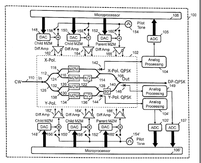
[0007] FIG. 1 illustrates a block diagram of one embodiment of a DP-QPSK
optical
transmitter according to the present teaching.
[0008] FIG. 2 illustrates one embodiment of an analog signal processor used
in the bias
control circuit of a DP-QPSK transmitter according to the present teaching
that is described in
connection with FIG. 1.
[0009] FIG. 3 illustrates graphs of the AC photodetector output power in
dBm and the
DC photodetector output current in milliamps, both as a function of the DC
voltage applied to
one of the child Mach-Zehnder modulators.
[0010] FIG. 4 illustrates graphs of AC output power of the envelope
detector in dBm and
DC output voltage of the envelope detector in volts both as a function of DC
bias voltage applied
to one of the parent Mach-Zehnder modulators.
[0011] FIG. 5 illustrates a flow chart of one embodiment of a method of
stabilizing a DP-
3
CA 02879461 2015-01-15
QPSK transmitter according to the present teaching that performs switching as
well as
implements the digital closed loop controllers to bias stabilize the high data
rate optical
modulators, such as 100-Gb/s DP-QPSK optical modulator.
[0012] FIG. 6 illustrates a method of bias stabilizing the DP-QPSK
modulator according
to the present teaching.
[0013] FIG. 7A illustrates an experimental test apparatus for a DP-QPSK
transmitter
according to the present teaching.
[0014] FIG. 7B illustrates experimental results as eye diagrams of X and Y
polarized
QPSK signals and for the combined DP-QPSK signal that were generated using the
experimental
test set apparatus for a DP-QPSK transmitter that is shown in FIG. 7A.
Description of Various Embodiments
[0015] Reference in the specification to "one embodiment" or "an
embodiment" means
that a particular feature, structure, or characteristic described in
connection with the embodiment
is included in at least one embodiment of the teaching. The appearances of the
phrase "in one
embodiment" in various places in the specification are not necessarily all
referring to the same
embodiment.
[0016] It should be understood that the individual steps of the methods of
the present
teachings may be performed in any order and/or simultaneously as long as the
teaching remains
operable. Furthermore, it should be understood that the apparatus and methods
of the present
teachings can include any number or all of the described embodiments as long
as the teaching
remains operable.
4
CA 02879461 2015-01-15
[0017] The present teaching will now be described in more detail with
reference to
exemplary embodiments thereof as shown in the accompanying drawings. While the
present
teachings are described in conjunction with various embodiments and examples,
it is not
intended that the present teachings be limited to such embodiments. On the
contrary, the present
teachings encompass various alternatives, modifications and equivalents, as
will be appreciated
by those of skill in the art. Those of ordinary skill in the art having access
to the teaching herein
will recognize additional implementations, modifications, and embodiments, as
well as other
fields of use, which are within the scope of the present disclosure as
described herein.
[0018] The present teaching relates to methods and apparatus for
implementing a digital
time division multiplexed optical transmitter for transmitting high data rate
DP-QPSK signals
over long-haul fiber optic networks. Some methods and apparatus according to
the present
teaching use lock-in stabilization of lithium niobate-based time division
multiplexed optical
transmitter for high data rate transmission. For example, transmitters
according to the present
teaching can generate DP-QPSK signals at 100-Gb/s for transmission over long-
haul fiber optic
networks. The DP-QPSK modulation format is particularly attractive for high
data rate optical
transmission (100-Gb/s and higher) in metro areas networks as well as long
haul fiber-optic
networks.
[0019] A high data rate DP-QPSK optical transmitter according to the
present teaching is
described as having a Mach-Zehnder type optical modulator which has two
parallel Mach-
Zehnder type superstructures. A first Mach-Zehnder type superstructure is used
for a first
polarization. A second Mach-Zehnder type superstructure is used a second
polarization. Each of
the two parallel Mach-Zehnder superstructures includes two parallel child Mach-
Zehnder optical
modulators. One skilled in the art will appreciate that numerous types of Mach-
Zehnder
CA 02879461 2015-01-15
modulators can be used, such as Mach-Zehnder modulators formed of lithium
niobate, Mach-
Zehnder modulators formed of Ill-V compound semiconductors, such as GaAlAs on
GaAs, and
Mach-Zehnder modulators formed of 1I-VI semiconductor, such as 1nP.
[0020] FIG. 1 illustrates a block diagram of one embodiment of a DP-QPSK
optical
transmitter 100 according to the present teaching. The DP-QPSK optical
transmitter 100
includes a DP-QPSK modulator 102 and associated hardware that differentially
drives the
modulator 102 components under microprocessor control. Many aspects of the
optical
transmitter of the present teaching is described in connection with the D-QPSK
modulation
format. However, one skilled in the art will appreciate that the transmitter
and methods of
transmitting according to the present teaching can be used with numerous other
types of
modulator formats, such as BPSK, m-ary QAM, m-ary PSK, OFDM, and any dual-
polarization
variant of these modulations forms. In addition, some aspects of the DP-QPSK
optical
transmitter 100 are described in connection with Mach-Zehnder modulators
(MZMs) and more
particularly described in connection with lithium niobate-based Mach-Zehnder
modulators.
However, one skilled in the art will appreciate that other types of
modulators, such as electro-
absorption modulators, can be used with the transmitter according to the
present teaching.
[0021] Lithium niobate-based Mach-Zehnder modulators have certain desirable
features
for high data rate transmitters, such as being stable against numerous types
of environmental
variations so that they can generate very reliable and repeatable high data
rate transmissions at
100 Gb/s and higher. In particular, lithium niobate-based Mach-Zehnder
modulators can have
highly stable operation under large operating temperature variations. In one
aspect of the optical
transmitter of the present teaching, the DP-QPSK lithium niobate optical
modulators are
stabilized using various lock-in techniques, which can be performed
automatically under
6
CA 02879461 2015-01-15
microprocessor control. Analog signal processors 104, 104' and microprocessors
106, 106' are
used to determine the various operating points of the parent and child Mach-
Zehnder modulators.
[0022] The DP-QPSK optical transmitter 100 includes an outer Mach-Zehnder
modulator
108 that includes an optical input 110 that receives an optical beam from a
laser source. In many
embodiments, the laser source is a tunable laser source. A first arm of the
outer Mach-Zehnder
modulator 112 includes a first parent Mach-Zehnder modulator 114. The first
parent Mach-
Zehnder modulator 114 includes a first child Mach-Zehnder modulator 116 that
is optically
coupled into a first arm 118. A second child Mach-Zehnder modulator 120 is
optically coupled
to a n/2 optical phase shifter 122 and optically coupled into a second arm
124. The first parent
Mach-Zehnder modulator 114 modulates a QPSK signal with a first polarization.
[0023] A second arm 126 of the outer Mach-Zehnder modulator 108 includes a
second
parent Mach-Zehndcr modulator 128 that includes a first child Mach-Zehnder
modulator 130
optically coupled into a first arm 132. A second child Mach-Zehnder modulator
134 is optically
coupled to a n/2 optical phase shifter 136 and optically coupled into a second
arm 138. An
optical polarization rotator 140 is also optically coupled into the second arm
126 of the outer
Mach-Zehnder modulator 108. In some embodiments, the optical polarization
rotator 140 is a
fixed n/2 polarization rotator. In other embodiments, the optical polarization
rotator 140 is a
variable polarization rotator. The second parent Mach-Zehnder modulator 128
modulates a
QPSK signal with a second polarization. The outer Mach-Zehnder modulator 108
multiplexes
the first and second polarization embedded into a dual-polarization QPSK
signal generation.
[0024] In one specific embodiment, the first and second parent Mach-Zehnder
modulators 114, 128 and each of the first and second child Mach-Zehnder
modulators 116, 120,
7
CA 02879461 2015-01-15
130, and 134 are all lithium niobate based Mach-Zehnder modulators. In this
embodiment, the
four individual child Mach-Zehender modulators 116, 120, 130, and 134 are
driven by an
electrical NRZ signal with a peak-to-peak voltage swing of 2V5 and biased at
the point of
minimum transmission to generate four PSK signals. In other embodiments, some
of these
modulators are other types of Mach-Zehnder modulators such as III-V or II-V
semiconductor
Mach Zehnder modulators. In yet other embodiments, electro-absorption
modulators can be
used instead of Mach-Zehnder modulators. In these embodiments, the first and
second parent
Mach-Zehnder modulators 114, 128 are biased at the quadrature point to
generate QPSK signals
in first and second polarization.
[0025] A first optical detector 142 is optically coupled to an output of
the first parent
Mach-Zehnder modulator 114. The first optical detector 142 detects the QPSK
signal generated
by the first parent Mach-Zehnder modulator 114 with the first polarization. A
second optical
detector 144 is optically coupled to an output of the second parent Mach-
Zehnder modulator 128.
The second optical detector 144 detects the QPSK signal generated by the
second parent Mach-
Zehnder modulator 128 with the second polarization. The first and second
optical detectors 142,
144 can be any type of optical detectors as long as the detectors have the
desired optical-to-
electrical conversion bandwidths. For example, the first and second optical
detectors 142, 144
can be PIN photodetectors with an optical-electrical bandwidth of a least 1
GHz and with an
optical-electrical coupling efficiency of at least 0.05%. In some embodiments,
a third
photodetector 146 can be optically coupled to an output of the DP-QPSK optical
modulator 102.
The additional third photodetector 146 may be used to lock-in stabilize the
variable polarization
rotator 140 used to generate the dual-polarization signal. Thus, one feature
of the optical
transmitter of the present teaching is the direct/indirect detection of AC
terms using
8
CA 02879461 2015-01-15
photodetector that may be built into the optical modulators.
[0026] One aspect of the present teaching is the hardware and software
that implements
various analog processors and digital controllers that are used to stabilize
and track various
operating points of the DP-QPSK optical modulator 102. The various analog and
digital
controllers can be pure integral controllers or can be proportional-integral
controllers. These
controllers are feedback controllers which calculate an "error" value as the
difference between a
measured process variable and a desired setpoint. The controllers attempt to
minimize the error
by adjusting the process control inputs. Proportional-integral controllers can
operate in a
proportional mode, an integral mode, or a proportional-integral mode.
[0027] The bias control circuit includes the analog signal processors 104,
104' and the
microprocessors 106, 106' for each polarization. In this embodiment, two
microprocessors 106,
106' are used for control. However, in other embodiments, only one
microprocessor can be
used. The analog signal processor 104 includes an analog input that is
electrically connected to
the output of the first photodetector 142. Similarly the analog signal
processor 104' includes an
analog input that is electrically connected to the output of the second
photodetector 142. The
analog-to-digital converters 105, 105' convert the output signals from the
analog processors 104,
104' to digital signals that can be processed by the microprocessors 106,
106'. The
microprocessors 106, 106' each have three digital outputs that are
electrically connected to
digital-to-analog converters 148, 148', 150, 150', 152, 152'.
[0028] The outputs of the digital-to-analog converters 148, 148', 150,
150', 152, 152'are
coupled to inputs of respective adder circuits 156, 156', 158, 158', 160,
160'. The output of pilot
tone generators 154, 154' that generate pilot tone signals are electrically
connected to other
9
CA 02879461 2015-01-15
inputs of the adder circuits 156, 156', 158, 158', 160, 160'. The outputs of
the adder circuits
156, 156', 158, 158', 160, 160' are electrically connected to respective
inputs of differential
amplifier 162, 162', 164, 164', 166, 166'. Each of the differential amplifiers
162, 162', 164,
164', 166, 166' include an output and inverse output that are electrically
connected to bias inputs
of a respective child or parent Mach-Zehnder modulators as shown in FIG. I.
That is, each child
and parent Mach-Zehnder modulator is biased by an output and an inverse output
of a respective
differential amplifier to increase the output voltage swing in order to
satisfy the end-of-life drive
voltage requirement.
[0029] More generally, the bias control circuit including the analog signal
processors
104, 104' and the microprocessors 106, 106' has a first and second input
electrically connected
to respective outputs of the first and second optical detectors 142, 144. A
first and second output
are electrically coupled to respective bias inputs of the first and second
child Mach-Zehnder
modulator 116, 120 of the first parent Mach-Zehndcr modulator 114. A third
output is
electrically coupled to a phase bias input of the first parent Mach-Zehnder
modulator 114. A
fourth and fifth output are electrically coupled to respective bias inputs of
the first and second
child Mach-Zehnder modulators 130, 134 of the second parent Mach-Zehnder
modulator 128. A
sixth output is electrically coupled to the phase bias input of the second
parent Mach-Zehnder
modulator 128. In embodiments that include the third photodetector 146
optically coupled to an
output of the outer Mach-Zehnder modulator 108, an output of the third optical
detector 146 is
electrically connected to an input of the bias control circuit 149 which in
turn is connected to
analog-to-digital converter 107.
[0030] The bias control circuit of the present teaching can include many
different
components such as the analog processors 104, 104' that generate voltages
which correspond to
CA 02879461 2015-01-15
DC photocurrents generated by the first, second, and third optical detectors
142, 144, and 146.
The bias control circuit can include analog-to-digital converters that covert
AC electrical signals
generated by the first, second, and third optical detectors 142, 144, and 146
in response to
modulated data to digital data. The microprocessors 106, 106' or other digital
processor(s)
acquire signals to determine bias signals that stabilize the optical
transmitter. In some
embodiments, bias control circuits according to the present teaching generate
electrical signals in
response to both DC and AC signals detected by the first, second, and third
optical detectors 142,
144, and 146. The bias control circuit monitors the pilot tone signals
generated by the pilot tone
generators 154, 154' that are received by the first, second, and third optical
detectors 142, 144,
and 146 and then generates bias control signals on at least one output that
sequentially stabilize
at least some of the Mach-Zehnder modulators in response to the monitored
pilot tone.
[0031] For DP-QPSK operation, the first and second parent Mach-Zehnder
modulators
114, 128 are biased at quadrature to establish a ic/2 phase shift between
signals generated by the
corresponding child Mach-Zehnder modulators 116 and 120, 130 and 134 so that
the first parent
Mach-Zehnder modulator 114 generates the QPSK signal with the first
polarization and the
second parent Mach-Zehnder modulator 128 generates the QPSK signal with the
second
polarization.
[0032] The bias control signals also stabilize the generated DP-QPSK signal
in response
to signals generated by the first, second, and third optical detectors 142,
144, and 146. In various
modes of operation, the bias control circuit generates electrical signals that
stabilize the first and
second parent Mach-Zehnder modulators 114, 128 to a quadrature point or to a
minimum
transmission point that minimizes DC and AC signals detected by the first,
second, and third
optical detectors 142, 144, and 146. In other embodiments, the bias control
circuit generates
11
CA 02879461 2015-01-15
electrical signals that suppresses or minimizes a fundamental harmonic of a
pilot tone applied to
a bias signal. Also, the bias control circuit generates electrical signals on
at least one output that
maximize average DC photocurrent generated by at least one of the first,
second, and third
optical detectors 142, 144, and 146.
[0033] The optical modulator structure in the transmitter 100 of FIG. 1 is
very sensitive
to the various operating bias points of the two parent Mach-Zehnder modulators
114, 128 and the
four child Mach-Zehnder modulators 116, 120, 130, 134 and these operating bias
points are
sensitive to environmental variations such as temperature. To build a reliable
optical transmitter
that operates at 100 Gb/s and above data rates that is stable against
temperature, will usually
require an automatic modulator bias control circuit that is controlled by a
microprocessor as
described here. One aspect of the present teaching is that the optical
transmitter of the present
teaching includes analog and digital signal processing that performs automatic
lock-in
stabilization of various bias points of the two parent Mach-Zehnder modulators
114, 128 and the
four child Mach-Zehnder modulators 116, 120, 130, 134.
[0034] To implement Time Division Multiplexed (TDM) lock-in stabilization
of the DP-
QPSK modulator, the output of the synchronous multiplier is directly sampled
at a rate which is
at least 20 times the fundamental frequency of a pilot tone using a high-speed
analog-to-digital
converter. This sampled signal is processed digitally in the microprocessors
106, 106' to
implement a digital controller which is an integral, proportional, or
proportional-integral
controller. The output of the digital loop controller is then directed to a
respective digital-to-
analog converter whose output is amplified by a differential driver amplifier
that drives the
respective child or parent MZMs embedded into a DP-QPSK modulator using high-
speed digital-
to-analog converters.
12
CA 02879461 2015-01-15
[0035] FIG. 2 illustrates one embodiment of an analog signal processor 200
used in the
bias control circuit of a DP-QPSK transmitter 100 according to the present
teaching that is
described in connection with FIG. 1. Referring to FIGS. 1 and 2, two analog
signal processors
are used the DP-QPSK transmitter 100 according to the present teaching. The
first analog signal
processor 104 has an input that is electrically connected to the output of the
first photodetector
142 and the second analog signal processor 104' has an input that is
electrically connected to the
output of the second photodetector 144. Thus, the first photodetector 142
detects the X-polarized
QPSK signal and the second photodetector 144 detects the Y-polarized QPSK
signal. The
following description of hardware and methods of operation is for one of the
analog signal
processors 104, 104'. However, it is understood that the hardware and methods
of operation is
the same for the other analog signal processor.
[0036] The photodetector 142 is terminated with a 50 Ohm impedance 202.
One aspect
of the present teaching is the use of a current mirror 204 that mirrors the DC
photocurrent of the
photodetector used to detect the QPSK modulated signal for each polarization.
A current mirror
circuit 204 is electrically connected in series with the photodetector 142.
The current mirror
circuit 204 generates a DC current that mirrors the DC photocurrent flowing
through the
photodetector 142. The current mirror circuit 204 accurately monitors the
average DC
photocurrent of the photodetector per polarization. The voltage corresponding
to this
photocurrent is then subtracted from the reference voltage and the resulting
voltage difference is
fed back into a synchronous multiplier with the directly detected AC term for
lock-in
stabilization of the four child Mach-Zchnder modulators 116, 120, 130, and
134. The output of
the current mirror 204 is the DC portion of the error signal of the X or Y
polarized QPSK signal,
which is the interference between the two modulated DPSK signals for each
polarization.
13
CA 02879461 2015-01-15
[0037] Another aspect of the present teaching is the use of indirect
detection of AC error
terms with a photodetector 142 followed by a high-speed electronic amplifier
206 and an
envelope detector 208 for each polarization. The envelop detector 208 is
switched in and out
whenever the parent Mach-Zehnder modulators 114, 128 are lock-in stabilized to
their
corresponding quadrature points. The DC output voltage of the envelop detector
208 along with
its AC counterpart is fed back into the synchronous multiplier. More
specifically, the output of
the photodetector 142 is electrically connected to a high-speed amplifier 206,
which amplifies
the AC portion of the error signal. The high-speed amplifier 206 has a
bandwidth that is high
enough to pass the AC error signal information. For example, the bandwidth of
the high-speed
amplifier 206 should be at least one 1 GHz for 100 GHz data transmission. In
addition, the
coupling efficiency for the high-speed amplifier 208 should be high enough to
pass enough
signal so that it can be processed by the analog signal processing hardware.
[0038] The output of the high-speed amplifier 206 is electrically connected
to a switch
210 that selects either the envelope detector 208 or a low pass filter 212 for
further processing.
The switch 210 is controlled by the microprocessor 106. In a first switch
position, the switch
210 selects a first signal path 214 through the envelope detector 208 for
processing the detected
X or Y polarized QPSK signal for stabilizing the phase. In a first switch
position, the switch 210
selects a second signal path 216 through a low pass filter 212 for stabilizing
each of the child
Mach-Zehnder modulators 116, 120, 130, and 134.
[0039] In the first signal path 214, the detected X, Y polarized QPSK
signal passes
through the envelope detector 208. The envelope detector 208 is an RF peak
detector, such as a
diode peak detector, that detects the DC and AC power carried by the input
signal. The envelope
detector 208 passes both a DC and an AC portion of the error signal. The
bandwidth of the
14
CA 02879461 2015-01-15
envelope detector 208 is chosen to be high enough to pass the AC portion of
the error signal
including the pilot tone. For example, the bandwidth of the envelope detector
208 is at least one
1 MHz in some systems that transmit data at 100-Gb/s.
[0040] The DC and AC portions of the error signal then pass through a
second low pass
filter 218 that is chosen to pass only the DC portion of the signal. For
example, the second low
pass filter 218 can be a 100 Hz low pass filter that essentially only passes
the DC error signal. In
addition, a second switch 220 when positioned in a first position couples a 10
kHz band pass
filter 222 to the output of the envelope detector 208 so that it passes only
AC error signals in the
kHz band, which includes the pilot tone signal. The second switch 220 is also
controlled by
the microprocessor 106.
[0041] In the second signal path 216, the detected X, Y polarized QPSK
signal passes
through the low pass filter 212. In one embodiment, the low pass filter 212 is
a 1 MHz low pass
filter that passes the DC portion of the error signal and the AC portion of
the error signal below
1 MHz. The second switch 220 is electrically connected a 10 kHz band pass
filter 222 in the
second signal path 216 when positioned in a second position. The 10 kHz band
pass filter 222
passes only error signals in the 10 kHz band, which includes the pilot tone
signal.
[0042] An adder circuit 224 is used to combine signals from the current
mirror 204,
envelope detector 208 and the low pass filter 212 in various ways depending
upon the switching
configuration. The adder circuit 224 includes a first input that is
electrically connected to the
output of a third switch 226 that selects between the 100 Hz low pass filter
218 and the output of
the current mirror 204. A second input of the adder circuit 224 is
electrically connected to output
of the 10 kHz band pass filter 222 that is electrically connected to the
output of the second switch
CA 02879461 2015-01-15
220.
[0043] The output of the adder circuit 224 is electrically connected to a
first input of a
multiplier 228. The output of the pilot tone generator 154 is electrically
connected to the delay
network 232 that delays the pilot tone signal in time. The output of the delay
network 232 is
electrically connected to the second input of the multiplier 228. The delay
generated by the
delay network 232 is adjusted so that only the error is detected at the pilot
tone frequency. The
output of the multiplier 228 is electrically connected to the analog-to-
digital converter 105
described in connection with the optical transmitter of FIG. 1.
[0044] For stabilizing the phase of the transmitter 100, the first switch
210 selects the
first signal path 214, where the second switch 220 electrically connects the
10 kHz band pass
filter 222 to the output of the envelop detector 208 and the third switch 226
electrically connects
the 100 Hz low pass filter 218 to the first input of the adder circuit 224.
The adder circuit 224
combines the DC portion of the signal detected by the envelope detector 208
that is filtered with
the 100 Hz low pass filter 218 with the AC portion of the signal detected by
the envelope
detector 208 that is filtered with the 10 kHz band pass filter 222. The
multiplier 228 multiplies
the broad band interference noise with a delayed reference pilot tone signal
to separate the
detected pilot tone from the rest of the broad-band interference noise. The
analog-to-digital
converter 105 converts the multiplied signal into a digital signal so that it
can be processed by
the microprocessor 106. In some methods of operation, whenever you switch from
the first
signal path 214 to the second signal path 216, the output of the analog-to-
digital converter 105 is
processed by the microprocessor 106.
[0045] FIG. 3 illustrates graphs 300 of the AC photodetector output power
in dBm 302
16
CA 02879461 2015-01-15
and the DC photodetector output current in milliamps 304, both as a function
of the DC voltage
applied to the child Mach-Zehnder modulators. These graphs 300 illustrate the
desired bias
condition for the child Mach-Zehnder modulators for the DP-QPSK transmitter of
the present
teaching. There are three AC minimums of the AC photodetector output power
that occur as the
bias voltage applied to the Mach-Zehnder modulator is increased from zero to
20 volts. The first
and third AC minimums occur when maximum transmission occurs and the
photodetector's DC
output current is at a maximum value. The bias conditions for maximum
transmission where the
photodetector's output current is a maximum occurs when the Mach-Zehnder
modulator bias
voltage is at 2 and 15 volts. The second AC minimum occurs at about 7 volts
when minimum
transmission occurs and the photodetector's output current is at a minimum..
The output power
of the modulator is about -30 dB for minimum transmission. Each of the Mach-
Zehnder
modulators is biased at their minimum transmission point where they are in a
DC off condition.
That is, the modulators are biased so that there are no NRZ signals driving
the modulator.
[0046] The graphs 300 of the AC photodetector output power in dBm 302 and
the DC
photodetector output current in milliamps 304 as a function of the DC voltage
applied to the
child Mach-Zehnder modulators show that if the transmitter were to monitor
only AC pilot tones
alone, the transmitter could lock onto the first or third AC minimums instead
of the second AC
minimum. Consequently, both the AC pilot tone and the DC photocurrent must be
monitored
simultaneously for each polarization to determine the correct bias point
stabilization for each of
the four child Mach-Zehnder modulators.
[00471 Thus, the characteristics of the graphs 300 shown in FIG. 3
illustrate that to bias
stabilize the child Mach-Zehnder modulators to minimum transmission, it is
necessary to both
suppress the fundamental harmonic of the pilot tone (AC) and to ensure that
the average DC
17
CA 02879461 2015-01-15
photocurrent of the photodetector is at its maximum value (DC) for proper lock-
in stabilization
when NRZ signals drive the respective child Mach-Zehnder modulator with a peak-
to-peak
voltage swing of 2V7,. In theory, one can use only the AC term, but then the
DC voltage range
has to be limited otherwise bias stabilization scheme could bring the
modulator to a point of
maximum transmission where the AC term once again goes through its minimum
value.
However, to satisfy the end-of-life DC bias voltage requirement of a 100-Gb/s
DP-QPSK
modulator, the operating DC bias voltage range cannot be restricted.
Therefore, it is necessary to
monitor both the AC term and the DC term while doing lock-in stabilization for
child Mach-
Zehnder modulators 116, 120, 130, and 134.
[0048] FIG. 4 illustrates graphs 400 of AC output power of the envelope
detector 208 in
dBm 402 and DC output voltage of the envelope detector in volts 404 both as a
function of DC
bias voltage applied to the parent Mach-Zehnder modulators. These graphs 402,
404 illustrate
the desired bias conditions of the parent Mach-Zehnder modulators for the DP-
QPSK transmitter
of the present teaching. The graph of AC output power of the envelope detector
402 is for the
pilot tone signal. In order to stabilize the phase of the parent Mach-Zehnder
modulator, both the
AC and DC output of the envelope detector 208 must be at a minimum. Thus,
according to the
graphs 402, 404, in order to stabilize the phase of the parent Mach-Zchnder
modulator, the DC
bias voltage should be locked at either 4, 11, or 17 Volts.
[0049] The graphs 400 of the AC output power of the envelope detector 208
in dBm 402
and the DC output of the envelope detector in volts 404 as a function of the
DC voltage applied
to the parent Mach-Zehnder modulators show that if the transmitter were to
monitor only AC
pilot tones alone, the transmitter could lock onto the wrong quadrature point
and hence polarity
of the modulated data at the output of the 100-Gb/s optical transmitter. That
is, both the DC and
18
CA 02879461 2015-01-15
AC output of the envelope detector 208 must be monitored simultaneously to
determine the
correct bias stabilization points so that the parent Mach-Zehndcr modulators
are stabilized to
their respective quadrature points.
[0050] Thus, the two parent Mach-Zehnder modulators 114, 128 are biased at
the
quadrature points to get the proper 90 degree optical phase shift between the
two PSK signals
generated by the corresponding two child Mach-Zehnder modulators 116 and 120,
130 and 134
to generate a QPSK signal for each of the X and Y polarizations. To bias
stabilize the two parent
Mach-Zehnder modulators 114, 128 to quadrature points, it is necessary to
minimize the DC
signal generated by the envelop detector 208 which measures the interference
between the two
modulated PSK signals. The interference is at a minimum when these two PSK
signals are
combined in phase quadrature (a desired QPSK signal) per polarization. Also,
it is necessary to
suppress the fundamental harmonic of the pilot tone (AC) which is indirectly
detected by the
envelop detector. In principle, only the DC voltage generated by the envelop
detector can be
monitored to bias stabilize the parent Mach-Zehnder modulators 114, 128, but
then the operating
DC voltage range must be restricted which is undesirable because the device
will not meet the
end-of-life requirement of a 100-Gbis optical modulator. Therefore, it is
necessary to monitor
both the DC and AC terms while performing lock-in stabilization for the parent
Mach-Zehndcr
modulators.
[0051] FIG. 5 illustrates a flow chart 500 of one embodiment of a method of
stabilizing a
DP-QPSK transmitter according to the present teaching that performs switching
as well as
implements the digital loop controllers to bias stabilize the high data rate
optical modulators,
such as 100-Gb/s DP-QPSK optical modulator. In many modes of operation, the
four individual
child Mach-Zehnder modulators 116, 120 130, and 134 are individually lock-in
stabilized at bias
19
CA 02879461 2015-01-15
points that generate four PSK signals. Also, the two parent Mach-Zehnder
modulators 114, 128
are lock-in stabilized at bias points which generate dual polarization QPSK
(PD-QPSK) signals
for transmission. Switching time division multiplexing using six different
proportional-integral
loop controllers is used for bias stabilization.
100521 Referring to FIGS. 1, 2, Sand 6, in a first step 502 of a method
according to the
present teaching, the analog signal processor 104 is initialized where the
analog and digital
inputs and outputs are configured. In a second step 504, the bias
stabilization algorithm is
initiated to acquire the relevant stabilization bias points of the DP-QPSK
modulator. In the
initial acquisition loop, the DP-QPSK modulator is lock-in stabilized using
time division
multiplexed digital loop controllers for at least ten iterations. That is, a
determination is made as
to what child or parent Mach-Zehnder modulator should be stabilized next
according to the
method 600 of bias stabilizing the DP-QPSK modulator of FIG. 6. For example,
the method can
first stabilize the first (I) and then second (Q) child Mach-Zehnder modulator
in the X
polarization, then stabilize the parent Mach-Zehnder modulator in the X
polarization, then
stabilize the first (I) and then second (Q) child Mach-Zehnder modulator in
the Y polarization,
then stabilize the parent Mach-Zehnder modulator in the Y polarization. In
some embodiments
described herein, each of the child Mach-Zehnder modulators 116, 120, 130, 134
and the parent
Mach-Zehnder modulators 114 and 128 are stabilized sequentially. However, in
other apparatus
and methods according to the present teaching, at least some of the child Mach-
Zehnder
modulators 116, 120, 130, 134 and the parent Mach-Zehnder modulators 114 and
128 are
stabilized in both the X polarization and Y polarization simultaneously.
10053] Referring now to FIG. 6, which is a method of bias stabilizing the
DP-QPSK
modulator according to the present teaching. The first step 601 sets the
polarization switch to
CA 02879461 2015-01-15
"1" ("1" for X-polarization and "2" for Y-polarization). The second step 602
sets the channel
switch to "1" for the I-Child MZM, "2" for the Q-Child MZM, and "3" for the
Parent MZM to
be stabilized. The third step 603 determines which Mach-Zehnder modulator in X-
polarization
or Y-polarization QPSK needs to be stabilized. The first (I) child Mach-
Zehnder modulator 604
for the X polarization is stabilized using the second signal path 216 in the
analog signal
processor 104. The fourth step 606 stabilizes the second (Q) child Mach-
Zehnder modulator for
the X polarization using the second signal path 216 in the analog signal
processor 104. The fifth
step 608 stabilizes the parent Mach-Zehnder modulator 114 for the X
polarization using the first
signal path 214 in the analog signal processor 104. This method is then
repeated for the Y
polarization.
[0054] The sixth step 610 stabilizes the first (I) child Mach-Zehnder
modulator 130 for
the Y polarization using the second signal path 216 in the analog signal
processor 104'. The
seventh step 612 stabilizes the second (Q) child Mach-Zehnder modulator 134
for the Y
polarization using the second signal path 216 in the analog signal processor
104'. The eighth
step 614 stabilizes the parent Mach-Zehnder modulator 128 for the Y
polarization using the first
signal path 214 in the analog signal processor 104'.
[0055] After each step, the state of the analog-to-digital signal processor
104, 200 and the
microprocessor 106 controlling the bias control circuits for the parent and
child Mach-Zehnder
modulators is switched in step 616. In an acquisition mode of operation, the
stabilization is
performed with the method 600 of bias stabilizing the DP-QPSK modulator for
three Mach-
Zehnder modulators (two child and one parent Mach-Zehnder modulator) for each
of the X and
Y polarizations. The process is then repeated for 10 times (step 506 in FIG.
5) for all child and
parent Mach-Zehnder modulator stabilizations.
21
CA 02879461 2015-01-15
[0056] The fourth step 508 is a decision step to determine if all the Mach-
Zehnder
modulators are stabilized or not using the method 600 of bias stabilizing the
DP-QPSK
modulator. If any of the Mach-Zehnder modulators can't be stabilized for some
reason, then an
acquisition error is issued in step 510. If all of the child and parent Mach-
Zehnder modulators
are stabilized to their respective points, the method is repeated in the
tracking mode of operation.
In the tracking mode of operation, the respective bias points of the child and
parent Mach-
Zehnder modulator are stabilized continuously on a time division multiplexed
basis as described
in connection with the method 600 of bias stabilizing the DP-QPSK modulator.
100571 In the first step 512 of the tracking mode of operation, the method
600 of bias
stabilizing the DP-QPSK modulator described in connection with FIG. 6 is
executed. A
determination is made as to what child or parent Mach-Zehnder modulator should
be tracked
next. For example, the method can first track the first (I) and then second
(Q) child Mach-
Zehndcr modulator in the X polarization, then track the parent Mach-Zehnder
modulator in the X
polarization, then track the first (I) and then second (Q) child Mach-Zehnder
modulator in the Y
polarization, then track the parent Mach-Zehnder modulator in the Y
polarization. In some
embodiments described herein, each of the child Mach-Zehnder modulators 116,
120, 130, 134
and the parent Mach-Zchnder modulators 114 and 128 are tracked sequentially.
However, in
other apparatus and methods according to the present teaching, at least some
of the child Mach-
Zehnder modulators 116, 120, 130, 134 and the parent Mach-Zehnder modulators
114 and 128 is
tracked in both the X polarization and Y polarization simultaneously.
[0058] In the second step 514 of the tracking mode of operation a decision
step is
performed to determine whether all four child and two parents Mach-Zehnder
modulators are
stable or not. If any one or more Mach-Zehnder modulator cannot be tracked for
their respective
22
CA 02879461 2015-01-15
bias points, then a tracking error is issued in step 516.
[0059] In the tracking modes of operation, whenever the operating
wavelength of the
integrated tunable laser assembly is changed by the network, the optical
phases of the parent
Mach-Zehnder modulators need to be reset. To facilitate this, a modulator bias
stabilization
algorithm reads the modulator bias reset input once in the third step 518. In
fourth step 520, the
decision is made depending on the logic state of the modulator bias reset
input. If the modulator
bias reset input is at logic '0' then the method 600 of bias stabilizing the
DP-QPSK modulator
performed in step 512 is executed as per tracking mode of operation. If the
modulator bias reset
input is at logic '1' then the optical transmitter's bias control circuit
automatically resets the
corresponding phases of the first and second parent Mach-Zehnder modulator
that generates
QPSK signals in first and second polarization so as to correctly set the X/4
phase difference in
response to a change in an operating wavelength of a tunable DP-QPSK optical
transmitter.
Also, the child Mach-Zehnder modulators 116, 120, 130, 134 have a small
wavelength
dependence on the DC bias. The bias signals to the child Mach-Zehnder
modulators 116, 120,
130, 134 can also be reset every time the wavelength changes. In addition, the
microprocessor
can be programmed to compensate for this wavelength dependence. Once the
digital loop
controllers are reset, then the modulator bias stabilization algorithm
automatically switches to
acquisition mode of operation.
[0060] FIG. 7A illustrates an experimental test apparatus 700 for a DP-QPSK
transmitter
according to the present teaching. The experimental test set apparatus 700 was
designed to
characterize a 100-Gb/s DP-QPSK signal generated with the DP-QPSK transmitter
and bias
control circuit according to the present teaching. The experimental test
apparatus 700 includes
an integrated tunable laser source 702 that generates CW optical power at its
output. The output
23
CA 02879461 2015-01-15
of the tunable laser source 702 is optically coupled to an input of a DP-QPSK
modulator 704
according to the present teaching, such as the DP-QPSK modulator 108 that is
described in
connection with FIG. 1.
[00611 A 625 MHz reference clock 706 is used to drive a multiplexer 708
that generates
the four 25 Gb/s signals that drive the four single-ended modulator driver
amplifiers 710 which
in turn drive the RF inputs of four child Mach-Zehnder modulators 116, 120,
130, and 134 as
described in connection with the optical transmitter of FIG. 1. The reference
clock 706 has a
clock rate that is 1/40th of the data rate. The output of the DP-QPSK
modulator 704 is optically
connected to an EDFA 712 that amplifies the modulated PD-QPSK optical signal.
The output of
the EDFA 712 is optically connected to a variable optical attenuator 714 that
attenuates the
modulated optical signal to a level appropriate for monitoring by an
oscilloscope 716. The
output of the variable optical attenuator 714 is optically coupled to the
oscilloscope 716, which
displays eye diagrams of the X, Y polarized QPSK modulated optical signals and
the combined
DP-QPSK optical signal.
[0062] FIG. 7B illustrates experimental results as eye diagrams of X and Y
polarized
QPSK signals and for the combined DP-QPSK signal that were generated using the
experimental
test set apparatus for a DP-QPSK transmitter that is shown in FIG. 7A. The
first eye diagram
750 shows a 25-Gb/s QPSK signal that is Y polarized. The second eye diagram
752 shows a 25-
Gb/s QPSK signal that is X polarized. The third eye diagram 754 shows the
multiplexed DP-
QPSK signal having four levels.
Equivalents
[0063] While the applicants' teaching is described in conjunction with
various
24
CA 02879461 2015-01-15
embodiments, it is not intended that the applicants' teaching be limited to
such embodiments.
On the contrary, the applicant's teaching encompass various alternatives,
modifications, and
equivalents, as will be appreciated by those of skill in the art, which may be
made therein
without departing from the spirit and scope of the teaching.