Note: Descriptions are shown in the official language in which they were submitted.
CA 02879526 2015-01-19
Optoelectronic Photo Sensor
CROSS-REFERENCE TO RELATED APPPLICATION: This
application is a
national stage patent application arising from PCT/RU2013/000995 filed on Nov.
8,
2013, and referenced in WIPO Publication No. W02014/081341. The earliest
priority
date claimed is Nov. 22, 2012.
BACKGROUND
[0001] The present invention relates to digital photographic technology, in
particular,
to optoelectonic systems (OES), and can be used to obtain mosaic digital
photographic images.
[0002] Known is an optoelectronic photo sensor, comprising a lens and a
digital
sensor located in the focal plane of the lens (China patent No. CN 101556758,
2010).
[0003] Also known is a digital camera with an optical system and a digital
electronic
sensor located in the focal plane of the optical system (US Application No.
2012/0082441, 2012).
[0004] The disadvantage of the known devices of this type is the small image
field
obtained due to the sizes of the sensor and the lens.
[0005] The closest technical solution to the method of the present invention
is an
optoelectonic photo sensor for aerial photography comprising an optical system
and
an electronic photosensitive device located on the focal surface of the system
(US
Application No. 2011/0122300, 2011).
[0006] The abovementioned known classical designs "one lens ¨ one matrix" have
limitations that are especially significant for aerial survey systems. The
size (and pixel
dimensions) of digital photo sensors is technologically and physically limited
and
practically every existing individual photo sensor has a smaller number of
photosensitive elements than any large-format film carrier in classical aerial
photography systems. Said disadvantage can be compensated in a monoscopic
1
CA 02879526 2015-01-19
system by using hybrid sensors based on several photo sensors with outputs
located
on three, two, or one crystal face (instrument case).
[0007] Although fairly capacious hybrid photo sensors are known in the art ¨
8,192x8,192 pixels (64 M), size129x129 mm, Loral Fairchild (USA), a hybrid of
8
matrices with single-side outputs; 8,192x8,192 pixels (64 M) size 90x90 mm,
Fortune
Aerospace (USA), a hybrid of 4 matrices with double-ended outputs ¨ the hybrid
approach is not promising for several reasons:
-- "mosaic" hybrid matrices with a minimum gap between mosaic elements
matching the complicated production process of the matrices themselves are
technologically complicated to manufacture;
--it is impossible to obtain resulting capacity of the sensor that would
exceed
the capacity of the initial matrices more than 4 to 5 times; and
--it takes a long time to read the composite picture (based on a preset
reading
rate) when using the required initial matrices with a maximum available
capacity and
to make preparations using the "frame readout" technology (which requires
mechanical shutters and a low framing rate, resulting in significant
limitation of the
carrier speed).
[0008] Multiple-lens aerial photography systems that synthesize resulting
images
(frame) from several simultaneously obtained base images (subframes) are free
from
the disadvantages inherent in hybrid photo sensors, and from some other
limitations
common for OESs having a "one lens ¨ one matrix" scheme. The most significant
feature of an OES with such a scheme is that each of the lenses forms its own
image
space (independent of the image spaces of other lenses) that participates in
framing
in conjunction with a three-dimensional overriding function, which is neither
smooth,
nor monotonous, nor continuous. Moreover, more problematic with the three-
dimensional function that generates a frame from subframes is that each point
in
each of the base image spaces (or at least in two adjacent base spaces) can
correspond to the same point of the native frame spaces. Thus, the subframe's
transformation into frames must be described in each particular case with one
generating function that refers to the class of piecewise-linear polynomial
transformations and rule sets for assigning one or another subframes space
(subareas) to a non-overlapping adjacent space (subareas) of the output frame.
2
CA 02879526 2015-01-19
[0009] Such approach to building photographic equipment is possible only in
digital photography, for example, when a picture is recorded onto a plane
covered
with photo-sensitive material, when integration of several pictures into one
frame
requires a secondary projection at a minimum, or, in simpler cases, when using
image transformers. In addition, photographic correction of the inevitable
image
distortions caused by the conjugation of several different scale images
located in
non-parallel focal planes is difficult, if not impossible. Conversely, for
digital images,
the task of piecewise-linear correction comes down to a calculation of base
picture
transformation into the initial one using a polynomial model with subsequent
formation of a single mosaic image. Concomitantly, with said calculations,
some
changes can be made to take into account (eliminate) the following:
- the slope of photographing axis to the landscape being depicted (perspective
distortions);
- the distortion of lenses used;
- the deviation of real focal distances from the theoretical (scale
correction);
and
- the relative position of lenses (for multiple-lens scheme).
[0010] Application of said approach to the building of systems with several
lenses and several matrices located thereunder can yield an optoelectronic
system
free from all or most of projection type constraints, provided that the
complex of
transformation functions is defined unambiguously. Thus, the output image can
be
obtained free from the perspective effect, can be adjusted to the theoretical
projection (frame, panoramic, etc.), and can include previously known space-
determined distortion presets listed in a table (grid-scale model).
SUMMARY
[0011] The technical result of the invention is an increased imaging format
of an optoelectronic photo sensor and reduced geometric and chromatic
distortions.
3
CA 02879526 2015-01-19
[0012] Said technical result is achieved by creating an optic system
comprising at least two lenses, while the photosensitive electronic device
comprises a plurality of individual groups of identical digital photosensitive
matrices corresponding to a plurality of lenses with a total number of all the
matrices not exceeding the number of lenses. The he matrices of each group are
located in a row with gaps not exceeding, in size, the product of the number
of
effective pixels multiplied by the actual pixel size in one matrix along the
symmetry axis thereof, oriented along a row, multiplied by the number of
groups
minus one. The groups of matrices are located in parallel rows with each on
the
focal surface of the corresponding lens in such a way that the matrices of one
group are displaced with respect to the matrices of another group along the
direction of their row to a distance not exceeding the length of the maximum
gap
between matrices in the row.
[0013] The second embodiment comprises an optic system having at least
two lenses, while the photosensitive electronic device comprises a plurality
of
individual groups of the same digital photosensitive matrices corresponding to
the plurality of lenses with the total number of all matrices not exceeding
the
number of lenses. The matrices of each group are located on the focal surface
of
the corresponding lens in a row with gaps along one axis comprising eponymous
symmetry axes of the matrices. The axes of the row of matrices from different
groups are located in parallel planes, whereupon projections of optic axes of
the
lenses form an angle, expressed in radians, and not exceeding the quotient of
the distance between adjacent matrices in the row divided by the product of
lenses' number multiplied by their focal distance.
[0014] The third embodiment has a characteristic condition, wherein the
matrices of one group are displaced with respect to the matrices of another
group along the direction of their row to a distance not exceeding the length
of
4
CA 02879526 2015-01-19
the maximum gap between the matrices in the row. The axes of the row of
matrices from different groups are located in parallel planes whereupon
projections of optic axes of the lenses form an angle, which size is inversely
proportional to the size of displacement of one group of matrices with respect
to
another. Said angle is expressed in radians and does not exceed the quotient
of
the distance between adjacent matrices in a row divided by the product of the
number of lenses multiplied by their focal distance. Said distinctive features
are essential.
[0015] A photo sensor with a plurality of identical lenses and rows of
staggered identical matrices, which are located on a shared focal surface with
gaps between adjacent matrices not exceeding the length of the effective pixel
number, and oriented along a row, creates a single large framing field from
many individual matrices. Such design contemplates the use of several small
individual lenses instead of one large and expensive lens as well as many
small
matrices instead of one expensive big matrix.
]0016] The features of the second and third embodiments also ensure
achieving the technical result.
[0017] Arrangement of lenses at an angle to each other and the strictly
defined dependence on the focal distance and the length of the gap between
matrices in a row ensure continuous imaging by individual matrices over the
surveyed surface with preset overlapping for subsequent cross-linking of
images
into one single film.
DRAWINGS
Fig. 1 shows a schematic representation of the first embodiment of an
optoelectronic photo sensor consisting of two lenses and four matrices.
CA 02879526 2015-01-19
Fig. 2 shows a scheme of eight matrices arranged in two groups of four
matrices for two lenses as per the first embodiment.
Fig. 3 shows a scheme of matrices arranged on two lenses as per the second
embodiment.
Fig. 4 shows a scheme of matrices arranged on two lenses as per the third
embodiment.
Fig. 5 shows an arrangement of lenses of optic axes for the second and third
embodiments.
DESCRIPTION OF PREFERRED EMBODIEMENT
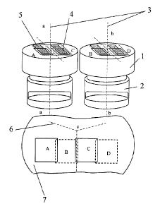
[0018] An optoelectronic photo sensor comprises holders 1 for lenses 2 with
optic
axes 3. Digital photosensitive matrices 4 are arranged on cards 5. Axes 3
jointly form
equivalent optic axis 6 of the optoelectronic photo sensor. The matrices form
a single
filed of the image on combined field 7 from individual images ABCD
corresponding to
the eponymous matrices 4.
[0019] Matrices 4
form individual groups ABCD and EFGH located on the focal
surface of corresponding lenses 2. Groups 9 of matrices 4 are arranged in a
row
along axis 8 with gaps not exceeding, in size, the product of the number of
effective
pixels multiplied by the physical size of a pixel of one matrix 4 along the
symmetry
axis thereof, oriented along the row, multiplied by the number of groups minus
one.
The groups of matrices are arranged in parallel rows ¨ each on the focal
surface of
the corresponding lens. Matrices 4 of one group ABCD are displaced with
respect to
matrices 4 of the other group EFGH along the direction of their row to a
distance not
exceeding the length of the maximum gap between the matrices in the row.
Provided
that the surveyed objects are located at a sufficient distance from the
lenses, an
image of the same scene will be formed on the focal planes of the lenses with
an
accuracy up to the observation parallaxes (linear, taking into account the
distance
between the lenses and, in general, angular, accounting for possible non-
parallelization of the optic axes) as an overlapping image formed by matrices
4 of the
group ABCD of combined field 7. If matrices 4 are arranged in groups of four,
the
image will consist of mated groups AEBFCGDH (Fig.2).
6
CA 02879526 2015-01-19
[0020] In the second and third embodiments, projections of optic axes 3 of
lenses 2 onto parallel planes comprising axes 8, form angle 10, expressed in
radians,
and not exceeding the quotient of the distance between adjacent matrices 4 in
a row
divided by the product of lenses' number multiplied by their focal distance.
In the third
embodiment, angle 10 is inversely proportional to the displacement distance of
one
group of matrices with respect to another, i.e. the third embodiment provides
a single
continuous view field when one row of matrices is displaced with respect to
another
to a distance not exceeding the length of the gap between matrices 4 in the
row.
[0021] The proposed optoelectronic photo sensor is equivalent to the
conditional lens with axis (c-c), wherein the view field thereof contains an
image,
which is practically identical to the image formed in the view fields of
lenses (a-a) and
(b-b) ¨ i.e., real lenses (a-a) and (b-b) repeat the scene visible in virtual
lens (c-c)
twice in the image space with the same focal distance and viewing angle as
those in
lenses 2.
[0022] Using at least two lenses instead of one is necessary to ensure a
continuous view field when employing real matrices wherein the size of
photosensitive area is significantly smaller than their full geometric
dimension
(due to the crystal case, lead frame and, actually, the outputs). The proposed
optoelectronic photo sensor uses a sensor, 6.38 x 5.26 mm in size, with the
diagonal of the reading workspace of 1:2.7 in., which corresponds to the
overall
view field dimensions of 5.53 x 4.09 mm, at an aspect ratio 4:3.
[0023] Said optoelectronic photo sensor is used in the following way:
[0024] As Fig. 1 shows, matrices A and C are fixed in holders 5 in the
focal plane of lens (a-a) at some distance from one to another, wherein said
distance is shorter than the overall dimensions of the matrix. Matrices B and
D
B are located in the focal plane of lens (b-b) in similar holders with a gap
in-
between as well. View fields (a-a), (b-b) and (c-c), disregarding parallaxes,
are
identical.
7
CA 02879526 2015-01-19
[0025] Alignment of said arrangement of sensor B in the view field of lens
(b-b) satisfies the condition of mating image B zone with image A zone with a
small (several dozen points) overlap, which is achieved because the holders of
matrices A and B are located in view fields of different lenses and move
independently, wherein 20 points with pixel size 3.275 i.im make about 0.06-
0.07 mm and linear alignment with such movements can be performed by
technical means.
[0026] Then, by fixing the position of matrices A-B, positions of matrix C
are aligned in the focal plane of lens (a-a) to achieve minimum overlapping
with
matrix B along the adjacent side. Then, similar alignment is performed for the
position of matrix sensor D with respect to focal plane (b-b). When a
satisfactory result is achieved, positions of holders 5 of matrices 4 are
mechanically fixed.
[0027] All aforementioned operations are performed under visual control
by observing view field (c-c), which jointly displays the data received from
all
matrices (optic sensors). The proposed device is technically feasible as long
as
the size of the matrix's visible area exceeds the size of the adjacent matrix
frames and holders 5, at least in the direction of assembling.
[0028] Optic characteristics of the lenses ensure a balanced size of the
matrix sensor and optic space resolution that is sufficient for placing four
matrices 4 under the lens onto unified holders 5. Respectively, the
optoelectronic photo sensor of such design will have a view field equivalent
to
view field 8 of adjacent matrices.
[0029] In the second embodiment, adjacent rows 9 of matrices may not be
displaced with respect to each other, i.e. groups of matrices 4 are arranged
in the
same way on all lenses 2. However, lenses 2 are tilted with respect to each
other
8
CA 02879526 2015-01-19
along axes 8. Axes 8 are intercrossed and lie in parallel planes. Projections
of
optic axes of lenses to these planes form angle 10, expressed in radians, that
does not exceed the quotient of the distance between adjacent matrices 4 in
the
row divided by the product of lenses' number multiplied by their focal
distance.
[0030] Similar to the first embodiment, matrices 4 form separate groups
ABCD and EFGH located on the focal plane of corresponding lens 2. Groups 9
of matrices 4 are arranged in a row along axis 8 with gaps in between. Groups
of
matrices are arranged in parallel rows ¨ each on the focal surface of the
corresponding lens. Provided that there is a specified angle between optic
axes
of the lenses, in the focal planes thereof there will be formed an image of
the
same scene as an overlapping image formed by matrices 4 of group ABCD of
combined field 7. If matrices 4 are arranged in groups of four, the image will
consist of mated groups AEBFCGDH (Fig.3).
[0031] The third embodiment reflects the intermediate position of matrices
and angles between optic axes of lenses, when angle 10 is inversely
proportional
to the displacement distance of one group of matrices with respect to another
(Fig. 4).
[0032] The proposed design of optoelectronic photo sensor provides one
single continuous view field of the surface surveyed from a plurality of
individual lenses and a plurality of individual matrices. Said design is
either
impossible to create with a single, however, large lens and a single large
matrix,
or, if created, would be unreasonably expensive and have extremely large
dimensions and weight.
9