Note: Descriptions are shown in the official language in which they were submitted.
CA 02879832 2015-01-06
Security element having a color-effect-producing structure
100011 This invention relates to a security element for an object of value,
said
element having a flat, transparent body with a front side and a back side
between
which there lies a center plane, a first region configured on the body and a
second
region configured on the body which encode a motif, said body having in the
first
region a ground element structure which conveys different color impressions
from
front and back sides in plan view of the body.
100021 Security elements of value documents having periodic line gratings
are
known, for example from DE 102009012299 Al, DE 102009012300 Al or DE
102009056933 Al. They can have color filter properties in the subwavelength
region when the grating is so designed with regard to the grating profile that
resonance effects occur in the visible wavelength region. Such color filter
properties are known both for reflective and for transmissive subwavelength
structures. Said structures have a strongly polarizing influence on the
reflection or
the transmission of an incident light ray. The color is relatively strongly
dependent
on angle in reflection or transmission of such subwavelength gratings.
However,
the color saturation is considerably weakened for said gratings when the
incident
light is unpolarized.
100031 There is known a line grating having subwavelength structures which
possesses angular-dependent, color-filtering properties. The line grating
possesses
a rectangular profile made of a dielectric material. The horizontal surfaces
are
overlaid with a high-refractive dielectric. Above this structure there is
likewise
located a dielectric material, with the refractive indices of the grating
substrate and
of the cover material preferably being identical. As a result there is formed
an
optically active structure consisting of two gratings made of the high-
refractive
material which are spaced by the height of the original rectangular profile.
The
grating ridges forming the line grating are made for example of ZnS. There can
be
produced therewith a color contrast in reflection, but in transmission a
change of
1
CA 02879832 2015-01-06
color tone for different angles is hardly perceptible. This structure is
therefore
only useful as a security feature in reflection and must be constructed on an
absorbent ground for that purpose.
[0004] Two-dimensionally periodic hole structures are described in the
scientific literature that have filter properties of the incident light in the
subwavelength region. In this connection, reference is made to the following
literature sources: T. W: Ebbesen et al., "Extraordinary optical transmission
through sub-wavelength hole arrays", Nature, 667-669 (1998); L. Martin-Moreno
et al., "Theory of extraordinary optical transmission through subwavelength
hole
arrays", Phys. Rev. Lett. 86(6), 1114-1117 (2001); W. L. Barnes et al.,
"Surface
plasmon subwavelength optics", Nature, Vol 424, Issue 6950, pp. 824-830
(2003);
J. Bravo-Abad et al., "How light emerges from an illuminated array of
subwavelength holes", Nature Physics 1, 120-123 (2006); H. S. Lee et al.,
"Color
filter based on a subwavelength patterned metal grating", Opt. Express 15,
15457-
15463 (2007); C.-P. Huang et al., "Dual effect of surface plasmons in light
transmission through perforated metal films", Phys. Rev. B 75, 245421 (2007).
Such so-called hole arrays consist of thin opaque metal films.
[0005] DE 102007016394 Al proposes employing such structures as security
elements in value documents for authenticating genuineness.
[0006] Further, two-dimensionally periodic gratings are known that allow a
color filtering in primary colors, red, green, blue, with high color
saturation over a
relatively great viewing-angle range. The publication B.-H. Cheong et al.,
"High
angular tolerant color filter using subwavelength grating", Appl. Phys. Lett.
94,
213104 (2009) describes a grating with cube-shaped elevations which has a
pronounced band-pass filter characteristic. The elevations are made of
amorphous
silicon and located on a glass substrate. A replication method for such
gratings is
presented in the publications E.-H. Cho et al., "Two-dimensional photonic
crystal
color filter development", Opt. Express 17, 8621-8629 (2009) and E.-H. Cho et
2
CA 02879832 2015-01-06
at., "Nanoimprinted photonic crystal color filters for solar-powered
reflective
displays", Opt. Express 18, 27712-27722 (2010).
[0007] The prior art further includes WO 2003/070482 Al, WO 2011/032665
Al, WO 2011/082761 Al, WO 2011/066992 Al, EP 2228671 Al. The
publications R. J. Potton, "Reciprocity in optics", Rep. Prog. Phys. 67, 717
(2004);
R. Petit, "Electromagnetic theory of gratings", Vol 22 of Topics in current
physics,
Springer-Verlag (1980), explain the principle of reciprocity in optics, in
particular
for gratings.
[0008] The grating structures from the prior art can be employed for
security
elements for protecting value documents, since they provide a color effect in
plan
view that is not reproducible by conventional copying methods. The angle
dependency of the color effect is especially advantageous therefor.
[0009] The invention is based on the object of developing a security
element
of the type stated at the outset so as to further increase the anti-forgery
security.
[0010] This object is achieved, in a first variant, by a security element
for an
object of value, which has: a flat, transparent body having a front side and a
back
side between which there lies a center plane, a first region configured on the
body
and a second region configured on the body which encode a motif, wherein the
body has in the first region a ground element structure which conveys
different
color impressions from front and back sides in plan view of the body, wherein
the
body likewise has the ground element structure in the second region, but in a
form
mirrored relative to the center plane, causing first and second regions to
show the
motif from both sides in plan view, but the motif to be unrecognizable in
transmission view.
[0011] The object is achieved, in a second variant, by a security element
for an
object of value, which has a flat, transparent body having a front side and a
back
side, a first region configured on the body and a second region configured on
the
3
CA 02879832 2015-01-06
body which encode a motif, wherein the body has a grating ground structure
which is filled with a first layer from the front side and with a second layer
from
the back side, and which conveys different color impressions from front and
back
sides in plan view,
- wherein the grating ground structure is the same in the first and in
the second
region, and in the first region the first layer has a first refractive index
and
the second layer a second refractive index,
- and in the second region the first layer has the second refractive
index and
the second layer the first refractive index, causing first and second regions
to
show the motif from both sides in plan view, but the motif to be
unrecognizable in transmission view.
[0012] The invention
provides in both variants a security element that shows a
colored motif from both front and back sides in reflection. However, said
motif
disappears completely in transmission even for different viewing angles. The
security element allows a fine design of motifs and can be manufactured by
standard embossing methods. Unless reference is expressly made to one of the
two
variants hereinafter, the following statements will apply equally to both
variants.
[0013] The invention
utilizes the universally valid law of reciprocity of the
optical path in a surprisingly manner. For the transmission of an optical path
through a medium it is thus irrelevant in which direction different layers are
passed through. Since the ground element structure is the same in the first
and
second regions with regard to the layers or structures present, the security
element
has no motif in the transmission mode. However, since in the first and second
regions the ground structures are inverted against each other relative to the
center
plane in the first variant, and the order of layers inverted in the second
variant,
different color impressions for the two regions result from front or back side
in
plan view, which encodes the motif.
4
CA 02879832 2015-01-06
[0014] The ground element structure can be embodied in different ways.
Thus,
in the first variant, it is possible to realize the ground element structure
by a
substrate having different interference layers on its cover surfaces. The
ground
element structure can also be realized by a grating ground structure in the
first
variant. When a grating ground structure is referred to in the following
description
of the first variant, this is to be understood only by way of example.
[0015] With regard to the grating ground structure, the effect of the
security
element is not restricted only to periodic structures. Quasi-statistical
structures can
also be employed, as long as such structures, which likewise constitute
grating
ground structures for the purposes of this invention for both variants, convey
different color impressions from front and back sides.
[0016] In the first variant, the mirroring of the ground element structure
on the
center plane interchanges front and back sides for the second region. Thus,
first
and second regions differ both from front side and from back side in plan
view.
Since in transmission the same layers are passed through in both the first and
second regions and the order of said passage is irrelevant for the
transmission due
to the physical principle of reciprocity, the first and second regions do not
differ in
transmitted light.
[0017] The invention provides in both variants, starting out from per se
known
ground element structures, e.g. grating structures, a security element that
shows a
motif in plan view which disappears in transmissive viewing. Such an effect
cannot be imitated with conventional copying methods, thereby giving the
security
element high anti-forgery security.
[0018] Grating ground structures that convey different color impressions
from
front and back sides in plan view can be produced especially simply by the
grating
ground structure being asymmetrical relative to the grating plane.
CA 02879832 2015-01-06
[0019] In the first variant, the mirroring of the grating ground structure
on the
center plane then corresponds to the producing of the inverse grating
structure.
The first and second regions can thus be characterized, in this embodiment of
the
first variant, by a grating structure being employed in the first region, and
the
inverse or negative form thereof being used for the grating in the second
region.
[0020] The mirroring operation for the second region leads of course to a
discontinuity on the boundary between the first and second regions. There can
therefore optionally be provided a transition zone between first and second
regions
which is smaller than a grating period and in which the grating ground
structure of
the first region runs into the mirrored form of the second region.
[0021] Especially good color effects in plan view result with grating
structures
that are not substantially greater than the wavelength. It is therefore
preferred that
the grating ground structure has a grating period of 100 nm to 1000 nm.
Especially
good color effects are shown by subwavelength gratings, so that a grating
period
between 200 nm and 500 nm is preferred. Gratings are subwavelength gratings
for
the purposes of the invention when the individual grating elements are smaller
than the wavelength in the region of light.
[0022] The security element reveals the motif more clearly the more
different
the color effect is from the front and back sides in plan view, since, in the
first
variant, front and back sides of the ground element structure are interchanged
in
the second region relative to the first region in order to produce the motif.
An
especially good difference between front-side view and back-side view is then
obtained in a grating ground structure that is overlaid with a thin metal
layer, a
semimetal layer or a high-refractive layer with a partly absorbent effect.
[0023] Examples of an asymmetrical grating ground structure are grating
elements that are trapezoidal or triangular in profile.
6
CA 02879832 2015-01-06
[0024] The first and second regions can in turn be patterned further. This
can
be obtained especially simply by the grating ground structure being two-
dimensionally periodic. Such a structure is furthermore especially forgery-
proof,
because it is hard to manufacture with the usual tools available to forgers.
[0025] This also holds for grating ground structures having cuboid
elevations
and depressions.
[0026] Preferably, the grating ground structure in a 2D-periodic embodiment
has a contiguous high-refractive (in particular metallic) ground layer which
defines a grating plane, and over the ground layer a two-dimensionally regular
pattern of individual high-refractive (in particular metallic) surface
elements
which respectively extend parallel to the grating plane and are respectively
spaced
from the ground layer by an interlevel dielectric or an intermediate layer by
a
distance that is greater than the thickness of the ground layer and of the
surface
elements. Optionally, the regular pattern has a periodicity between 100 nm and
800 nm, preferably between 200 nm and 500 nm, in at least two directions
extending parallel to the grating plane.
[0027] The grating structure provides in the 2D-periodic embodiment further
preferably a high-refractive ground layer as well as high-refractive surface
elements which are disposed over the ground layer. The high-refractive
property
of the ground layer and of the surface elements is obtained by a suitable
choice of
material. Besides metal as a material, one might consider in particular
silicon or
silicon monoxide. In this description the term "metallic" is understood to be
equivalent to "high-refractive", unless expressly described otherwise.
[0028] It is essential for the effect of this embodiment that a contiguous
metallic layer has disposed thereover non-contiguous surface elements disposed
in
a pattern. When a two-dimensionally periodic grating with a profile possessing
perpendicular flanks is metal-vapor-coated perpendicularly, a non-closed metal
film arises on plateaus on the grating's upper side. On the lower grating
surface
7
CA 02879832 2015-01-06
(ground layer) a contiguous metal film forms. The elevations of the profile
are
overlaid with metal only on the plateaus.
[0029] The non-vapor-coated grating structure optionally consists of a
dielectric material having e.g. a refractive index of about 1.5. Plastic
foils, e.g.
PET foils, are particularly suitable as a substrate. The actual base structure
is e.g.
likewise configured in plastic, preferably UV lacquer. After vapor coating,
the
structure finally is filled with UV lacquer and laminated with a cover foil.
Thus a
layer construction is present wherein the upper and lower sides possess
substantially the same refractive index.
[0030] Further, the coating is not only restricted to simple metallic
layers.
Multiple layers, in particular trilayers, are also conceivable. It is known
that
multiply coated one-dimensionally periodic gratings enable a strong color
filter
filtering through the formation of Fabry-Perot resonators both in reflection
and in
transmission. In trilayers the following layers are particularly preferred:
two
semitransparent metal layers with an interjacent dielectric spacer layer, or
two
high-refractive layers with an interjacent low-refractive layer. For the metal
layers
the following materials come into consideration: Al, Ag, Pt, Pd, Au, Cu, Cr
and
alloys thereof. Suitable high-refractive layers are for example ZnS, ZnO,
Ti02,
ZnSe, SiO, Ta205 or silicon. As low-refractive layers, Si02, A1203 or MgF2
might
be used.
[0031] In an especially expedient manufacturing method, a dielectric is
first
patterned suitably as a base structure and then coated. Then the ground layer
has
an opening in the region under each surface element. This is advantageous at
the
same time, since an optical effect then also arises in transmission.
[0032] It is preferred that the grating is embedded into an embedding
dielectric
which has the same refractive index as the dielectric which forms the base
structure and spaces the ground layer from the surface elements. The
refractive
index can lie for example between 1.4 and 1.6.
8
CA 02879832 2015-01-06
[0033] It has turned out that the color effects of the grating ground
structure
can be influenced by the periodicity of the pattern. This can be utilized for
producing colored symbols or images. For this purpose, the surface filling
factor
and/or the distance between surface elements and ground layer can be varied
locally. In particular, it is possible to design a group of a plurality of
surface
elements with identical dimensions such that a desired color effect occurs.
This
group then forms a subpixel. A plurality of subpixels are designed with
different
color properties through corresponding geometrical design and then combined
into
a pixel. This allows a colored image representation. The different colors can
be
varied through the corresponding local variation of one or more of the
parameters
of the grating (distance of the surface elements in two spatial directions as
well as
distance of the surface elements from the ground layer).
[0034] Through the pixel-wise color mixture of basic colors, e.g. RGB
colors,
in subpixel regions there can be produced true-color images. The advantage of
such structures over conventional printing technology is that a very fine
patterning
into the micrometer range can be performed here.
[0035] A ground element structure suitable for the first variant and
employing
no grating is a substrate with different interference layers disposed on its
cover
surfaces. Such a substrate can be simply formed into the security element by
suitably patterning front and back sides. It is only essential that the
reflection
behavior is different on the first and second cover sides for the interference
construction. This is obtained by the ground element structure being
asymmetrical
relative to the center plane, because the layers on the cover surfaces differ
in their
thickness or in their material composition or both. The layer construction is
consequently mirrored in the first region relative to the second region.
[0036] The regionally different patterning can be achieved with
conventional
methods, for example a washing method or by laser demetallization.
9
CA 02879832 2015-01-06
[0037] For the layers there come into consideration a multiplicity of
interference layers which differ with regard to their reflecting properties on
a
substrate. Thus, color-shift layer systems are suitable. Also, opaque layer
materials
can be employed which are present in partly perforated form in order to obtain
the
required transmission.
[0038] The employment of perforated layers has the advantage that the
layers
on front and back sides of the substrate can first be applied unpatterned and
are
then only processed differently with regard to their perforation in order to
form
first and second regions. The perforation can be carried out for example using
a
pulsed laser beam, etc.
[0039] To obtain a color effect in transmission, the substrate can be dyed.
[0040] The above-mentioned effect of the reciprocity of the optical path
also
holds in case different refractive indices are present on the boundary
surfaces of
the grating ground structure and the half-space located thereabove or
therebelow.
The second variant of the invention makes use of this, and can thereby employ
a
grating ground structure that is substantially the same in the first and
second
regions. The different color effect then arises only from the order of layers
that is
provided in the first region, i.e. the order of layers over the grating ground
structure and under the grating ground structure, being inverted in the second
region. The layer material located over the grating ground structure in the
first
region is disposed under the grating ground structure in the second region,
and
vice versa.
[0041] The security element can be employed for a value document. It can in
particular be integrated in a security thread, tear thread, security band,
security
strip, patch or label. In particular, the security element can span
transparent
regions or recesses of the value document.
CA 02879832 2015-01-06
[0042] The security
element can in particular be part of a precursor, not yet fit
for circulation, for a value document which can additionally have further
authentication features. Value documents are understood to be, on the one
hand,
documents that are furnished with the security element. On the other hand,
value
documents can also be other documents or objects that are furnished with the
security element in order for the value documents to have uncopiable
authentication features to enable an authenticity test and prevent unwanted
copies.
Chip cards or security cards, such as e.g. bank cards or credit cards or
identity
cards, are further examples of value documents.
[0043] It will be
appreciated that the features mentioned hereinabove and those
to be explained hereinafter are usable not only in the stated combinations but
also
in other combinations or in isolation without going beyond the scope of the
present invention.
[0044] Hereinafter
the invention will be explained more closely by way of
example with reference to the attached drawings, which also disclose features
essential to the invention. There are shown:
Figs. la-d different
views of a security element from the front side (Fig. I a),
the back side (Fig. I b), in transmission view (Fig. 1 c) and as a
sectional representation (Fig. I d),
Fig. 2 a sectional
representation through a design of the security element 20
of Fig. 1 which, according to a first variant of the invention, consists
of a grating ground structure and has two regions,
Figs. 3-5 sectional
representations similar to Fig. 2 for further embodiments of
the grating ground structure according to the first variant,
11
CA 02879832 2015-01-06
Fig. 6 a perspective schematic representation of the security element
having a further embodiment of the grating ground structure
according to the first variant,
Fig. 7 a sectional representation through the security element of Fig. 6,
Fig. 8 a perspective schematic representation of a further embodiment of
the grating ground structure of Fig. 6,
Fig. 9 a development of the grating ground structure of Fig. 8,
Fig. 10 a modification of the grating ground structure of Fig. 9,
Figs. 11-12 schematic representations to illustrate how the grating ground
structure according to the first variant works,
Figs. 13-17 diagrams relating to the filter properties of different grating
ground
structures,
Fig. 18 a schematic representation for the image production within one of
the regions,
Fig. 19 a sectional representation through a design of the security element
20
of Fig. 1 which consists of a ground element structure having an
interference layer construction,
Figs. 20-22 modifications of the design of Fig. 19, and
Fig. 23 a modification of the design of Fig. 4 for realizing a second
variant
of the invention.
10045] Fig. 1 shows different views of a security element 20 which serves
for
authentication or for copy protection of an object of value, for example a
value
document, such as a bank note, etc. The security element 20 provides different
12
CA 02879832 2015-01-06
views of one and the same motif from the front and back sides in plan view,
and
the motif disappears in transmission view.
[0046] Fig. 1 contains four subfigures showing the different views. Fig. 1
a
shows the view of the security element 20 from the front side. It can be seen
that a
motif in the form of a star stands out against a background 21. The foreground
22
forms the motif, in the example the star. The different hatching illustrates
that
foreground 22 and background 21 differ in plan view in color and/or play of
colors upon tilts and/or reflected intensity. Viewed from the front side, the
foreground 22, i.e. the star, appears in reflection e.g. in a different color
and
intensity from the background 21. When the security element 20 is viewed from
the back side there is obtained, as shown in Fig. 1 b, an inversion of the
color
impression and intensity impression for the foreground 22 and the background
21.
Color and intensity that the foreground 22 had on the front side appear for
the
background 21 upon viewing on the back side. The same holds accordingly for
the
background 21 on the front side and the foreground 22 on the back side.
[0047] In transmission view (Fig. 1c), however, the motif disappears
completely even for different viewing angles, since the colors of the star and
of
the background are identical. In Fig. I c the outline of the star is drawn in
only to
illustrate this effect. It does not appear, however, since color and intensity
are
identical for foreground 22 and background 21 in transmitted light.
100481 This effect of the security element 20 is by no means restricted to
two-
colored motifs in reflection. It is also possible to design a multicolored,
for
example four-colored, motif in reflection. Said motif would then appear in two
colors in transmission. In general, it holds that an n-colored motif appears
in
reflection through a corresponding design of the security element 20, which
will
be explained hereinafter, but in transmission as a structure with only n/2
colors.
[0049] The plan-view/transmission-view effect can be employed particularly
preferably with see-through windows of bank notes or other value documents.
The
13
CA 02879832 2015-01-06
color properties can hardly be imitated by simple means, but can be perceived
with
the unarmed eye without auxiliary means.
[0050] Further, it is possible to test the transmission properties, in
particular
the disappearance of the motif, by machine, for example with bank-note
processing or counting machines. This test can be done using a transmission
sensor which is equipped with a multicolored light source, for example a white
light source, and captures the transmission in a spatially resolved manner for
different wavelengths or different wavelength regions. A simplified variant is
also
conceivable, wherein the transmission is measured either for a wavelength or
as an
integral value for white light. In this manner it can be simply tested whether
no
motif is recognizable in transmission, which would not be the case with
conventional printing methods that could be used for imitating the color
effect in
plan view. The security element 20 can of course also be combined with other
structures, such as holograms, etc.
[0051] Fig. ld shows a schematic sectional representation through the
security
element 20 of Figs. 1 a to c. It can be seen that the security element 20
consists
throughout of a ground element structure G, with the ground element structure
being inverted in the region of the motif 21 relative to a center plane M
lying
between the cover surfaces of the security element 20. Said inversion can be a
complete mirroring around the center plane M. However, it is also possible
that
the inversion only relates to certain parameters of the ground element
structure G,
for example a sequence of refractive indices. Hereinafter a complete inversion
or
mirroring will be explained, in a first variant. A second variant will relate
to the
inversion of refractive indices.
[0052] The inversion is illustrated by the different hatching in the region
of the
foreground 22. In the case of a mirroring, it has the consequence that in the
region
of the background 21 a first cover side 25 of the ground element structure G
is
located above in the representation of Fig. id while a second cover side 26 is
14
CA 02879832 2015-01-06
located below. In the region of the foreground 22 the relations are exactly
inverted, i.e. the second cover side 26 is located above and the first cover
side 25
below. In both variants the reflecting properties that the ground structure G
has are
inverted in the region of the foreground 22 relative to the background 21 in
each
plan view. The transmission properties remain the same due to the law of
reciprocity.
[0053] The security element 20 produces a color effect through the
regionally
inverted ground element structure G, which shows different color effects from
the
front and back sides in plan view. Such ground element structures G are known
to
the skilled person in many forms. Hereinafter, different variants thereof will
be
explained.
[0054] Relative to the center plane M between front and back sides, which
corresponds approximately to the drawing plane in Fig. 1, the ground element
structure G is inverted between foreground 22 and background 21 in the first
variant. In other words, the structure in the background 21 and foreground 22
is
identical structurally, but not with regard to orientation. In the foreground
22 the
ground element structure is mirrored on the center plane M.
[0055] The ground element structure G has different reflecting properties
on
its two cover surfaces 25, 26. The different effects in the views of Figs. la
and lb
can thus be described, employing these terms, as follows, the description
assuming
the example of mirroring (first variant). It equally holds quite generally for
the
principle of the inversion of properties that are essential for reflection
behavior:
[0056] In Fig. la one sees for the background 21 the first cover side 25 of
the
ground element structure G. In the region of the foreground 22, i.e. of the
star, on
the other hand, one sees the second cover side 26 of the ground element
structure
G which is the same except for the orientation. The relations are inverted
from the
back side in plan view (Fig. 1 b). One thus sees for the background 21 the
second
cover side 26 and for the foreground 22 the first cover side 25. The ground
CA 02879832 2015-01-06
element structure G is the same in the total security element 20 except for
this
change of orientation. It is only mirrored on the center plane M in the
foreground
22 relative to the background 21, so that the motif is formed by regions I and
II in
which the first cover side 25 is visible for the background 21 and the second
cover
side 26 for the foreground 22 from the front side in plan view. Due to the
different
reflecting properties of the ground element structure G on the first and
second
cover sides 25, 26 there is obtained a clear recognizability of the motif.
[0057] Fig. 2 shows a schematic sectional representation through the
security
element 20 of Fig. 1, for a first embodiment of the ground element structure
G.
There are represented side by side the first region I ¨ corresponding to the
background 21 for example ¨ and the second region II ¨ corresponding to the
foreground 22 for example ¨ separated by a dashed line. The ground element
structure G is realized here as a grating ground structure 1. In both regions
I and II
the grating ground structure 1 is identical except for a transition region,
which is
already mentioned in the upper, general part of the description and will be
explained further hereinafter.
[0058] The grating ground structure 1 consists in this embodiment of
regular
grating ridges 23 and grating grooves 24. In the exemplary embodiment
according
to Fig. 2, the grating ridges 23 are triangular and the grating grooves 24
likewise.
To facilitate manufacture, the grating grooves 24 are filled with a material
whose
refractive index differs from that of the grating ridges 23. Said filling is
not
absolutely necessary, however. The grating ground structure 1 is so disposed
in
the region I that the first cover side 25 is located above in the
representation of
Fig. 2, and the second cover side 26 below. In the region lithe grating ground
structure 1 is aligned so as to be inverted thereto, i.e. mirrored on the
center plane
M, which is the grating plane here. As a result, in the region lithe first
cover side
25 is located below in the representation of Fig. 2, and the second cover side
26
above.
16
CA 02879832 2015-01-06
[0059] The grating ground structure 1 reflects radiation incident on the
first
cover side 25 as reflected radiation R1, and radiation incident on the second
cover
side 26 as reflected radiation R2. Since the reflecting properties differ on
the first
and second cover sides in the grating ground structure 1, the reflected
radiations
R1 and R2 consequently also differ in the regions I and II. The motif,
consisting of
foreground 22 and background 21, thereby becomes visible.
[0060] In the transmitted-light mode, on the other hand, the transmitted
radiation T does not differ in the regions I and II, since in both regions the
same
structures are passed through and the order of passage is irrelevant due to
the law
of reciprocity of the optical path.
[0061] It is an essential property of the ground element structure G that
it is
not symmetrical with regard to its reflecting properties relative to the first
and
second cover sides. In the case of a grating this is obtained by the grating
ground
structure 1 likewise being asymmetrical with regard to the grating's center
plane.
This is the case in Fig. 1.
[0062] From the point of view of manufacturability, it is preferable to
employ
an asymmetrical grating ground structure 1 for the security element 20, since
such
a structure can be simply replicated by an embossing method. Hence, relief
gratings are preferably suitable having grating ridges 23 and grating grooves
24
that are asymmetrical relative to the grating's center plane and whose surface
is
vapor-coated, for example with metal. Fig. 3 shows such a rectangular grating
in a
representation similar to Fig. 2. In the region II the mirrored profile of the
region I
is again present. The grating has different reflecting properties but the same
transmission in the regions I and II. Relative to the grating's center plane,
asymmetrical grating profiles are preferably formed by rectangular gratings
with a
filling factor that deviates considerably from 0.5. At a value of exactly 0.5
an
inversion or mirroring between the regions I and II would not be possible.
17
CA 02879832 2015-01-06
[0063] It is simpler to manufacture by an embossing method a trapezoidal
profile as is shown schematically in Fig. 4. With such a grating it is also
possible ¨
and this is also represented in Fig. 4 ¨ for the flanks to be overlaid with a
thin
layer, for example a thin metal film, upon a directional vapor coating or
deposition. Even then the transmission T remains the same for the regions I
and II.
The same also holds in the case of an oblique angle deposition on such a
profile
form.
[0064] Fig. 5 finally illustrates the general case of a grating ground
structure 1
that is asymmetrical with regard to the grating's center plane, and has a
mutually
mirrored arrangement in the regions I and II.
[0065] The grating ground structure 1 can be configured one-dimensionally.
However, two-dimensionally periodic gratings have the advantage that a
substantially stronger asymmetry in the filling factor can be formed, which
effectuates even clearer differences between the reflection on the first cover
side
25 and the second cover side 26. An especially good contrast in the motif
between
foreground and background is the consequence. Fig. 6 shows schematically such
a
two-dimensional periodic grating whose basic principles will be explained more
closely hereinafter with reference to Figs. 8 to 19.
[0066] Upon viewing from the upper side, mirroring or specular reflections
can occur intrusively under unfavorable conditions. The color properties of
the
described grating ground structure in reflection can be improved by an
additionally applied scattering foil, as Fig. 4 shows. Therein the grating
ground
structure l is embedded into a carrier 2 which has reflection-diminishing
properties on its cover surfaces, for example through a suitable scattering
foil.
Preferably, such a scattering foil has a relatively small angular divergence
lying
for example between 50 and 200. This scattering effect can also be achieved by
particles in a UV lacquer or in a cover foil or in the carrier 2. The uniform
transmission is practically unimpaired by the light scattering, provided the
18
CA 02879832 2015-01-06
scattering behavior of the carrier 2 or of the layers or foils applied thereon
is
approximately the same on both cover sides.
[0067] In the security element 20 the grating ground structure 1 is the
same in
the regions I and II except for an inversion or mirroring in one of the
regions. This
leads to there having to be a transition region at the boundary between the
regions
I and II, where the grating ground structure 1 runs into its mirrored form.
Said
transition is illustrated in Figs. 2b to 7 by a dashed line. The transition
region
where the ground structure 1 runs into its inverted, i.e. mirrored, form has
an
extension in the region of a period of the grating structure, which is
imperceptible
to the unarmed eye due to the employed structure sizes with periods of 1000 nm
or
less.
[0068] With reference to Figs. 8 to 19 the two-dimensional periodic grating
structure of Fig. 6 will hereinafter be explained more closely. The figures
relate
here only to the grating ground structure, i.e. the configuration in the
region I or II.
[0069] Fig. 8 shows a grating ground structure 1 which can be employed for
the security element 20 in a value document. The grating ground structure 1 is
manufactured by the carrier 2 being furnished with a profile possessing
perpendicular flanks. The profile is so configured that a pattern 6 of pillars
4 is
formed on an upper side of the carrier 2. The carrier consists of a dielectric
and
was coated with a metal layer which is deposited in a ground layer 3 on the
surface of the carrier 2 as well as in a coating 5 on the pillars 4. Due to
the
perpendicular flanks the latter are uncoated.
[0070] In principle, the grating ground structure 1 is so configured that
it is not
completely opaque in the transmitted-light mode, i.e. remains light-
transmissive to
a certain degree. The layer thickness T of the metal layer is therefore chosen
accordingly, as is the material.
19
CA 02879832 2015-01-06
[0071] In the pattern 6 the pillars 4, which are configured as cuboid here
only
by way of example and may be, inter alia, cylindrical (not necessarily
circular
cylindrical) elevations, are disposed in the form of a two-dimensionally
periodic
grating, with periodicities pi and p2 being present along two mutually
perpendicular directions in the grating plane of the grating ground structure
1, said
plane being defined by the ground layer 3. The extensions of the pillars 4 or
of the
elevations in the ground plane are designated as si and s2. The ground layer 3
as
well as the coatings 5 have a layer thickness t. The coatings 5 disposed in
the
pattern 6 are spaced from the upper side of the ground layer 3 by the distance
h - t
through the height h of the pillars 4. The pillar height h of the profiled
carrier 2 is
greater than the layer thickness t, so that the metal layer is interrupted and
the
coatings 5 are not contiguous. There thus arises a metal structure consisting
of the
ground layer 3 which defines the grating plane, with holes 8 over which the
coatings 5 are located. The distance between the coatings 5 and the ground
layer 3
is effectuated by the dielectric pillars 4.
[0072] The periodicities pi and p2 preferably lie in the subwavelength
region,
i.e. in the region between 100 nm and 1000 nm, preferably between 200 nm and
500 nm. The filling factors si/pi and 52/132 lie between greater than 0.5 and
0.8,
preferably under 0.7. To achieve a color filtering independent of
polarization, the
profile parameters are chosen identically for the two spatial directions if
possible,
i.e. pi = p2 and si = s2. This is optional, however. Likewise, the directions
of
periodicity are mutually perpendicular in the described exemplary embodiment.
This too is optional. Spatially asymmetrical arrangements of the profile and
of the
periodicity are also conceivable. In other words, the pattern 6 need not be a
Cartesian pattern, as represented in Fig. 8. Also, the pillars 4 can be
designed
asymmetrically.
[0073] Fig. 9 shows a development in which the grating ground structure 1
is
embedded into an embedding dielectric 7. This has use-related advantages,
since
the surface of the grating ground structure 1 is then smooth.
CA 02879832 2015-01-06
[0074] Fig. 10 shows a grating ground structure 1 whose pillars 4 are of
circular cylindrical configuration. This form is particularly suited for
unpolarized
light. Modifications of the square form of Fig. 8 or circular form of Fig. 10
are
likewise possible, e.g. through rounded corners for example.
[0075] Figs. 11 and 12 show how the grating ground structure 1 works. Fig.
11
shows the relations upon incident radiation E on the upper side 9 in the
region I.
Fig. 12 shows the incidence in the region II. The security element reflects
incident
radiation E in the form of reflective radiation R and transmits a portion as
transmitted radiation T. The essential difference between the illumination in
the
region I and in the region II is that, in the region I, the incident radiation
E first
falls on the periodic coating 5 disposed in the pattern 6. In the region II,
on the
other hand, the pattern of the holes 8 in the ground layer 3 is illuminated
directly.
This difference has clear consequences in reflection behavior, in particular
with
regard to color impression.
[0076] Through the application of the metal layer to the patterned carrier
2, the
ground layer 3 is furnished with the holes 8 under the coatings 5, i.e. in the
region
of the pillars 4. The grating ground structure 1 thus has a so-called hole
array in
the metal layer 3, with the arrangement of the holes 8 being defined by the
pattern
6. When the flanks of the pillar 4 are completely perpendicular, the
arrangement
and sizes of the holes 8 correspond exactly to those of the coatings 5.
[0077] The ground layer 3 of the design of Figs. 8 to 10 can be
supplemented
or replaced by multiple layers. The same holds for the coating on the pillars.
[0078] For manufacturing the grating ground structure 1 and thus the
security
element 20, different processes come into consideration. Manufacture is
simplest
when the dielectric carrier 2 with the elevations disposed in the pattern 6,
for
example pillars 4, and with the regions I and II is first formed and then
coated.
This can be effected either perpendicularly or by oblique angle deposition.
The
essential point is that the coatings 5 are not contiguous, i.e. are single.
21
CA 02879832 2015-01-06
[0079] For manufacturing the carrier 2 it is possible to use a casting
process,
so that a cost-efficient mass production can be realized.
[0080] The security element 20 described here obtains its coloration
through a
grating ground structure having a two-dimensional periodic subwavelength
structure in the zeroth diffraction order. The color-giving embossed
structures are
then especially color-intensive, can be disposed in an accurately positioned
manner relative to other embossed security structures, and appear in the
desired
uniform color tone from a relatively wide viewing angle in plan view.
[0081] Possible parameters of two-dimensionally periodic gratings are:
Structure p [nm] s [nm] h [nm] t [nm]
a) 400 120 300 40
b) 240 117 300 40
c) 330 167 300 40
d) 400 203 310 40
e) 240 117 300 20
[0082] The structures a) - e) were cast on PET foils in UV lacquer, vapor-
coated with aluminum and subsequently laminated with a PET foil. The
refractive
index of the PET foil and of the UV lacquer amounts to about 1.56 in the
visible.
[0083] Fig. 13 shows transmission behavior and reflection behavior for
structure a). The reflection response on the first cover side is designated as
RI, the
reflection response on the second cover side as R2, and the transmitted
radiation
as T. The figures respectively show the intensity I as a function of
wavelength.
The metal employed was aluminum with a layer thickness t of 40 nm. Fig. 14
shows the responses for the structure b), Fig. 15 for the structure c), and
Fig. 16
for structure d).
22
CA 02879832 2015-01-06
[0084] Said grating ground structures show different colors both in
reflection
and in transmission. The reflection on the first cover side differs quite
clearly from
the reflection on the second cover side. This stands out most clearly with the
structures c) (Fig. 15) and d) (Fig. 16). Fig. 15 demonstrates a red color
tone on
the first cover side, while the second cover side appears blue. The
transmission, on
the other hand, is blue viewed from both sides. The structure d) of Fig. 16,
however, appears reddish on the first cover side, turquoise on the second
cover
side, and green in transmission. The angular tolerance of the color tone was
examined by reflection measurements at different angles of incidence. Fig. 17
shows the reflection of the structure e) for the angles of incidence 8 (curve
13),
300 (curve 15) and 45 (curve 14). The reflection maximum lies in the blue for
this structure, shifting only slightly upon a variation of the angle of
incidence. The
structure always appears blue for these different angles of incidence.
[0085] The above-described profile-dependent coloration can be utilized to
produce colored symbols or images within one of the regions. Fig. 18 shows
three
portions 17, 18, 19 of a grating ground structure of different profile (PR,
SR, hR),
(PG, sG, hG) and (pB, 5B, hB) which appear in the colors, red, green and blue.
These
different colors can be evoked through the corresponding variation of one or
more
profile parameters.
[0086] The three portions 17, 18, 19 correspond to RGB subpixels and
together form a pixel 16. In each portion 17, 18, 19 the respective profile
ensures
that the corresponding colors, red, green and blue, are effectuated. At the
same
time, through the choice of profile one can adjust the share that the color of
the
respective RGB subpixel formed by the portion 17, 18 or 19 has in the pixel
16. It
is thus possible to give the pixel 16 a desired color. The color mixture of
the
primary colors that is effectuated in the pixel 16 through the portions 17,
18, 19 of
the RGB subpixels thus makes true-color images possible. The advantage of such
a structure over a conventional printing method is that a very fine patterning
into
the micrometer range is possible, which is advantageous in particular with
23
CA 02879832 2015-01-06
magnification arrangements. The grating ground structure 1 according to Fig.
12
allows microimages wherein the grating profile changes laterally in order to
achieve a contrast in color or intensity in the microimage. The structure
described
here is preferably suited therefor, since its optical properties are very
angle-
tolerant, i.e. its color hardly changes upon a variation of the angle of
incidence.
This property is advantageous for a combination with microlens arrays, since
the
light perceived by a viewer stems from different optical paths having
different
angles of incidence.
100871 In the regions I and lithe images then differ only with regard to
their
play of colors in plan view; while these differences disappear in transmitted
light.
100881 For the security element 20 subwavelength gratings are preferably
suited, i.e. grating ground structures 1 having grating elements (for example
grating ridges 23 and grating grooves 24) at least one of which is smaller
than the
wavelength of light. The manufacture of such structures is usually done by
photolithographic methods. Interference lithography or mechanical scratching
is
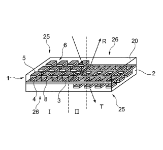
also possible. An original is finally manufactured that is subsequently copied
over,
galvanically or using photopolymers (e.g. Omocers), to an embossing stamp with
which the carrier 2 is then embossed. Subsequently, the carrier 2 is suitably
coated
and, where applicable, furnished with lamination layers.
[00891 The manufacture of the security element 20 with regions I and II of
the
grating ground structure 1 that are mirrored on the grating plane can be done
by
assembling the first region of an original with an impression of said
original. The
embossing stamp can be manufactured in this way as well. The copies of the two
regions can be produced e.g. by the exposure of a film made of photopolymers
through a mask, and subsequently assembled in a further copying step. The
corresponding inversion can of course also already be provided in the
original.
24
CA 02879832 2015-01-06
[0090] For embossing the carrier 2 there can be employed a continuous
embossing process for embossing a foil. For this purpose, an embossing
cylinder
is usually fabricated.
[0091] Fig. 19 shows a schematic sectional representation of a further
possible
form of realization for the security element 20. Here, there is employed as a
ground element structure G an interference construction which is executed here
as
a three-layer construction having a substrate 27 and two semitransparent metal
layers 28 and 29. In the regions I and lithe ground element structure is
mutually
mirrored relative to the center plane, so that the first cover side 25 is
located
above, in the representation of the figure, in the region I but the second
cover side
26 in the region II. The same holds accordingly for the sides located below.
As a
result, the first metal layer 28 is located above for the region I in the
image of Fig.
19, but below for the region II. Due to reciprocity the transmission is
identical in
both regions, while the reflecting properties differ, thereby making the motif
recognizable.
[0092] It should be pointed out that the step that is to be seen in the
substrate
27 between the regions I and II is not present in reality. It merely
illustrates the
mirroring of the ground structure G in the regions I and II. In reality, the
substrate
27 runs through and only the layers 28 and 29 change. This regionally
different
patterning can be achieved by a washing method or also by laser
demetallization.
In so doing, the region II is first masked and the layer sequence for the
region I
applied, for example by a vapor deposition method. In the next step the region
I is
masked and the layer sequence of the region II vapor-deposited.
[0093] It is also conceivable that one of said metal layers is perforated.
This
embodiment can be seen in Fig. 20. In known color-shift layer systems, the
lower
layer is usually designed as an opaque mirror layer. To obtain a transmission,
however, said mirror layer can be present in partly perforated form. The
semitransparent metal layer 28 is homogeneous, the mirror layer 29 perforated.
CA 02879832 2015-01-06
Said perforation can be produced using a pulsed laser. Alternatively, there
can be
employed a washing method, a metal transfer method or a so-called lift-off
method.
[0094] Fig. 21 shows a ground element structure G wherein both layers 28
and
29 are made of the same material and have the same thickness. They are only
perforated differently, giving rise to the different reflecting properties.
The
manufacture of this variant is especially simple, since the individual layers
can be
applied successively in laterally unpatterned form and over the full surface.
The
perforation is then performed using a pulsed laser. This is possible on both
sides.
Alternatively, the perforation can be effected unilaterally after one metal
layer has
been applied and then after the other metal layer has been applied..
[0095] Fig. 22 shows a modification of the design of Fig. 19. Here, the
security element is inverted in the regions I and II with regard to its
refractive
index structure and not mirrored with regard to the geometry.
[0096] The security element 20 of Fig. 22 has a dielectric 33 which
respectively has a metallization 34, 35 on its front and back sides. Over the
metallization 34 there is applied a cover layer 31, and under the
metallization 35 a
lower layer 32.
[0097] The cover layer 31 has two layer portions 36 and 38, with the layer
portion 36 lying in the region I and the layer portion 38 in the region II.
Likewise,
the lower layer 32 is patterned accordingly, so that it has a layer portion 37
in the
region I and a layer portion 39 in the region II. The layer portions 36 and 39
have
the same refractive index nl. Likewise, the layer portions 37 and 38 have the
same
refractive index n2 differing from the refractive index n1 . Thus, the same
layers
are present in the region I as in the region II, but inverted with regard to
their
refractive index structure. This leads to an interaction of the incident light
in the
regions I and II even in the case of a plane, semitransparent metal layer
construction. In the region I the layer system, formed by the layers 33 to 35,
26
CA 02879832 2015-01-06
borders upwardly on the layer portion 36 with the refractive index n1 and
downwardly on the layer portion 37 with the refractive index n2. In the region
II
the refractive indices are interchanged from the front and back sides. This
leads to
a different reflection behavior in the two regions. The transmission is
identical,
however.
[0098] Boundary surfaces with different refractive indices can be
manufactured by vapor deposition or by printing different dielectrics. The
measures described above with reference to the other embodiments are all
suitable
here, too, for adjusting laterally different layer portions with desired
refractive
indices.
[0099] In Fig. 22, cover layer 31 and lower layer 32 are represented with
the
same geometry. This is not compulsory. Thus, the cover layer 31 can in fact
have a
different structure or thickness from the lower layer 32.
[0100] Fig. 23 shows a design according to the possibility of designing a
security element that was designated as the second variant at the outset.
Here, as
also in Fig. 22, an inversion is provided with regard to the refractive index
structure and not with regard to the geometry (as in the first variant). The
security
element 20 of Fig. 23 has a grating structure 30 which is furnished with a
metallization 34. The cover layer 31 disposed over the grating structure 30
fills the
grating structure. The same holds for the lower layer 32 lying on the other
side.
[0101] The grating structure 30 is represented by way of example as a
relief
grating of trapezoidal cross section. However, there can be employed all of
the
grating structures described here, also the grating structures mentioned in
connection with the first variant. Unlike the first variant, it is now not
(exclusively) a variation of the profile form of the grating structure 30 that
produces the different reflection behavior in the regions I and II, but rather
a
change in refractive index. The cover layer 31 has different refractive
indices,
namely the refractive indices nl and n2, in the layer portions 36 and 38. In
the
27
CA 02879832 2015-01-06
lower layer 32 the refractive indices are exactly inverted thereto, so that
the layer
portion 37 has the refractive index n2 and the layer portion 39 the refractive
index
n I . Thus, a different reflection behavior is achieved with a grating
structure 30
that is homogeneous in the regions I and II, since the refractive-index jump
between the layer portion 36 and the combination of metallization 37 and
grating
structure 30 shows a reflection behavior on the front side in the region I
that
corresponds to that on the back side in the region II. The same holds
accordingly
for the front side of the region II and the back side of the region I. Unlike
the
above-described first variant, it is thus not the geometry in the regions I
and II that
is interchanged in the second variant, but rather the arrangement of the
refractive
indices.
[0102] It is of course possible to combine the measures of the first
variant and
of the second variant, so that the different reflection behavior from front
and back
sides and the difference between the regions I and II that is no longer
recognizable
in transmission can be obtained both by an inversion of the geometry and by an
inversion of the refractive index cross section.
[0103] In principle, the substrate 27 can be dyed in order to produce a
colored
effect in transmission.
28
CA 02879832 2015-01-06
List of reference signs
1 Grating
2 Carrier
3 Ground layer
4 Pillar
Coating
6 Pattern
7 Dielectric
8 Hole
9 Front side
Back side
11, 12 Multilayer construction
13, 14, 15 Curve
16 Pixel
17, 18, 19 Portion
Security element
21 Background
22 Foreground
23 Grating ridge
24 Grating groove
First cover side
26 Second cover side
27 Substrate
28, 29 Interference layers
Grating structure
31 Cover layer
32 Lower layer
33 Dielectric
34, 35 Metallization
29
CA 02879832 2015-01-06
36-39 Layer portion
Pillar height
Ground element structure
Center plane
Coating thickness
s1 Pillar width
S2 Pillar depth
131, P2 Period
A Surface normal
Incident radiation
Reflected radiation
RI Reflected radiation
R2 Reflected radiation
Transmitted radiation