Note: Descriptions are shown in the official language in which they were submitted.
CA 02880402 2015-01-27
WO 2014/028472 PCMJS2013/054706
CONTROL SIGNAL PROTECTION DEVICE
FIELD OF THE INVENTION
[0001] The present invention relates generally to control signals for
controlling field
devices in a process control system, more particularly, to a method and
apparatus for
preserving control signals.
DESCRIPTION OF THE RELATED ART
[0002] Process control systems, such as those used in chemical, petroleum and
other
processes, generally include one or more centralized or decentralized process
controllers
communicatively coupled to at least one host workstation, and to one or more
process control
and instrumentation devices, via analog, digital, or combined analog/digital
buses. Field
devices such as valves, valve positioners, switches, transmitters, and sensors
(e.g.,
temperature, pressure, or flow rate sensors) perform various functions within
the process,
such as opening or closing valves or measuring process parameters. The process
controller
receives (via the communication buses) signals indicative of process
measurements or
process variables made by or associated with the field devices, implements a
control routine
based on the received information, and generates control signals which are
sent over one or
more of the buses to the field devices to control the operation of the
process. Information
from the field devices and the controller is typically made available to one
or more
applications executed by a host workstation to enable an operator to perform
desired
functions with respect to the process, such as viewing the current state of
the process,
modifying the operation of the process, etc.
[0003] "Smart" field devices that perform one or more process control
functions have
become prevalent in the process control industry. In addition to performing a
primary
function within the process (e.g., monitoring a temperature or controlling a
valve position),
each smart field device includes a memory and a microprocessor. The memory
stores data
pertaining to the device, and the microprocessor communicates with the
controller and/or
other devices, and/or performs secondary tasks such as self-calibration,
identification,
diagnostics, etc. A number of standard, open, digital or combined digital and
analog
communication protocols such as the Highway Addressable Remote Transducer
(HART ),
PROFIBUS , FOUNDATION' TM Fieldbus, WORLDFIP , Device-Net , and Controller
- 1 -
CA 02880402 2015-01-27
WO 2014/028472 PCT/US2013/054706
Area Network (CAN) protocols have been developed to enable smart field devices
made by
different manufacturers to communicate with one another while performing one
or more
process control functions.
[0004] Control signals are typically provided to field devices via
input/output (1/0) cards
that convert control signals to a desired format suited for the particular
field devices to which
the control signals are being provided. In order to improve control system
robustness, control
systems sometimes employ redundant I/0 cards for controlling a field device.
In such control
systems, operation is switched from a primary 110 card to a back-up 1/0 card
in an event of
failure of the primary 1/0 card. Such redundant 1/0 card configuration
generally allows a
process being controlled to continue functioning without any significant
interruption when an
IJO card fails to operate properly. In some systems, an 1/0 card controller is
configured to
switch 1/0 card operation from the primary 1/0 card to the back-up 1/0 card
periodically for
verification of functionality of the back-up 1/0 card. I/0 card switchover
from a primary I/0
card to a back-up 1/0 card (or vice versa) typically results in a short
interruption in the
control signal provided to the field device. Some field devices respond to the
control signal
interruption in an undesirable manner. For example, if the field edvice being
controlled is a
valve, a valve controller may control the valve to move to an undesired
position, potentially
disrupting the process.
SUMMARY
[0005] In accordance with a first exemplary aspect .a control signal
protection device
operates in a first or in a second operational mode. In the first operational
mode, the control
signal protection device stores energy in a power storage element in the
control signal
protection device. In the second operational mode, the control signal
protection device
utilizes the stored energy to sustain a control signal at the output of the
device in an event of
an interruption in the control signal at the input of the device. In one
embodiment, the signal
protection device includes a switching circuit to control operational mode of
the device. In
an aspect, the control signal protection device further includes an input
current monitoring
element that controls the switching circuit. In this respect, the input
current monitoring
circuit may cause the device to switch from the first operational mode to the
second
operational mode when input current to the device is below a threshold, and
may cause the
device to transition from the second operational mode to the first operational
mode when the
- 2 -
CA 02880402 2015-01-27
WO 2014/028472 PCT/US2013/054706
input current is above the threshold. In some embodiments, the control signal
protection
device includes a voltage monitoring element to monitor a voltage level at the
output of the
device. In this aspect, when operating in the second operational mode and in
the absence of a
control signal at the input to the device, the device may maintain output
voltage at the voltage
level indicated by the voltage monitoring element.
[0006] In further accordance with the first exemplary aspect, the control
signal protection
device may further include, in any combination, any one or more of the
following preferred
forms.
[0007] In one preferred form, the power storing element includes at least one
capacitor.
[0008] In another preferred form, the power storing element includes a first
capacitor and a
second capacitor, and electric energy is supplied to the output terminals from
the first
capacitor and from the second capacitor.
[0009] In another preferred form, the switching circuit controls the
operational mode in
response to variation in input current entering the signal protection device.
[0010] In another preferred form, the control signal protection device
according further
comprises a current monitoring circuit. The current monitoring circuit causes
the control
signal protection device to transition from the first operational mode to the
second operation
mode when current entering the signal protection device is below a threshold
value, and
causes control signal protection device to transition from the second
operational mode to the
first operational mode when current entering the signal protection device is
above the
threshold value. In one preferred form, the threshold value is 2mA.
[0011] In another preferred form, the control signal protection device further
comprises a
voltage maintaining element to maintain a filtered and scaled version of
voltage
corresponding to a voltage level across the input terminals during the normal
operational
mode.
[0012] In another preferred form, the voltage across the output terminals is
maintained at
the filtered voltage in the second operational mode.
[0013] In another preferred form, the first operational mode is a normal mode
in which the
control signal is provided at the input terminals, and wherein the second
operational mode is
a protection mode in which the control signal is not provided at the input
terminals.
- 3 -
CA 02880402 2015-01-27
WO 2014/028472 PCT/US2013/054706
[0014] In accordance with a second exemplary aspect, a method of protecting a
control
signal provided to a field device in a process control system involves
providing a host station
and communicatively coupling the host station to a plurality of input output
(1/0) cards
including a first card and a second card, wherein operation is selectively
switched from the
first card to the second card. The method also involves providing a control
signal from the
host station via the first card or the second card to a control signal
protection device. The
control signal protection device switches from a first operational mode to a
second
operational mode during a transition of operation from the first card to the
second card. In an
embodiment, the control signal protection device stores electric energy in a
power storing
element in the first operational mode, and supplies electric energy stored in
the power storing
element is to an output terminal of the control signal protection device in
the second
operational mode.
[0015] In further accordance with the first exemplary aspect, the method may
further
include, in any combination, any one or more of the following preferred forms:
[0016] In one preferred from, the control signal protection device stores
electric energy in
a power storing element in the first operational mode, and supplies electric
energy stored in
the power storing element is to an output terminal of the control signal
protection device in
the second operational mode.
[0017] In another preferred form, storing electric energy in the power storing
element
comprises storing energy in a first capacitor and in a second capacitor, and
supplying electric
energy comprises transferring stored electric energy from the first capacitor
and from the
second capacitor to the output terminal of the control signal protection
device.
[0018] In another preferred form, causing the control signal protection device
to switch
from the first operational mode to the second operational comprises causing
the control signal
protection device to transition from the first operational mode to the second
operation mode
when current entering the signal protection device is below a threshold value,
and causing the
control signal protection device to transition from the first operational mode
to the second
operational mode when current entering the signal protection device is above
the threshold
value.
- 4 -
[0019] In accordance with a third exemplary aspect, a system for
controlling a field device
in a process control system comprises a host station and a plurality of
input/output (I/O) cards
coupled to the host station for providing a control signal to the field
device. The plurality of
I/O cards includes a primary I/O card and a back-up I/O card. The system also
comprises an
I/O card controller configured to selectively switch between the primary I/O
card and the
backup I/O card. A control signal protection device is communicatively coupled
to the I/O
cards and to the field device, wherein the control signal protection device
sustains the control
signal at an output of the signal protection device during a switchover
operation between the
primary card I/O card and the backup I/O card.
100201 In further accordance with the first exemplary aspect, the system may
further
include, in any combination, any one or more of the following preferred forms.
100211 In one preferred form, the control signal protection device is
configured to store
electric energy in a power storing element in a first operational mode, and
supply electric
energy stored in the power storing element to an output terminal of the
control signal
protection device in a second operational mode.
[0022] In another preferred form, the power storing element included at
least one
capacitor.
[0023] In another preferred form, the power storing element includes a first
capacitor and a
second capacitor, and electric energy is supplied to the output terminal of
the control signal
protection device from the first capacitor and from the second capacitor.
[0024] In another preferred form, the power storing element includes a charge
pump.
[0025] In another preferred form, the control signal protection device is
further configured
to monitor current level at an input terminal of the control signal protection
device, and
switch operation of the control signal protection device from the first
operational mode to the
second operational mode in response to detecting that the current level is
below a threshold
value.
[0026] In another preferred form, the control signal protection device is
provided as an
element separate from the field device.
- 5 -
CA 2880402 2019-10-11
10026a1 According to another aspect, a control signal protection device having
a first
operational mode and a second operational mode is provided. The control signal
protection
device includes a first terminal pair that connects the control signal
protection device to a
control system, wherein the control system provides a control signal to a
field device. The
control signal protection device further includes a second terminal pair that
connects the
control signal protection device to the field device, a power storing element
for temporary
accumulation of electric energy, a resistor to control a rate of accumulating
energy in the
power storing element, and a switching circuit for controlling operational
mode of the control
signal protection device. The electric energy is stored in the power storing
element in the first
operational mode without disturbing operation of a current loop connected to
the control
signal protection device and electric energy stored in the power storing
element is supplied to
a positive terminal in the second terminal pair in the second operational
mode.
[0026b] According to yet another aspect, a method of protecting a control
signal provided to
a field device in a process control system is provided. The method includes
the steps of
providing a host station; communicatively coupling the host station to a
plurality of input
output (I/0) cards including a first card and a second card, wherein operation
is selectively
switched from the first card to the second card; providing a control signal
from the host
station via the first card or the second card to a control signal protection
device; accumulating
energy at a controlled rate without disturbing operation of a current loop
connected to the
control signal protection device; and causing the control signal protection
device to switch
from a first operational mode to a second operational mode during a transition
of operation
from the first card to the second card, wherein the control signal protection
device sustains
the control signal at an output of the signal protection device during a
switchover operation
between the first card to the second card.
[0026c1 In a preferred form, causing the control signal protection device to
switch from the
second operational mode to the first operational mode includes causing the
control signal
protection device to transition from the second operational mode to the first
operational mode
when current entering the control signal protection device is above a
threshold value.
- 5a -
CA 2880402 2019-10-11
[0026d] According to yet another aspect, a control system for controlling a
field device in a
process control system is provided. The control system includes a host
station; a plurality of
input/output (I/O) cards coupled to the host station for providing a control
signal to the field
device, wherein the plurality of input/output (I/O) cards includes a primary
I/O card and a
back-up I/O card; an I/O card controller configured to selectively switch
between the primary
I/O card and the backup I/O card; and a control signal protection device
communicatively
coupled to the I/O cards and to the field device, wherein the control signal
protection device
accumulates energy at a controlled rate without disturbing operation of a
current loop
connected to the control signal protection device and sustains the control
signal at an output
of the signal protection device during a switchover operation between the
primary card I/O
card and the backup I/O card by storing electric energy in a power storing
element in a first
operational mode and supplying electric energy stored in the power storing
element to an
output terminal of the control signal protection device in a second
operational mode.
[0026e] According to yet another aspect, a control signal protection device
having a first
operational mode and a second operational mode is provided. The control signal
protection
device includes a first terminal pair that connects the control signal
protection device to a
control system, a second terminal pair that connects the control signal
protection device to the
field device, wherein the control system provides a control signal to the
field device via the
control signal protection device, a power storing element for temporary
accumulation of
electric energy from the control signal protection device, a resistor to
control a rate of
accumulating energy in the power storing element and a switching circuit,
within the control
signal protection device, for controlling operational mode of the control
signal protection
device, wherein a sufficiently small amount of electric energy is extracted
from a current loop
connected to the control signal protection device and stored in the power
storing element in
the first operational mode without disturbing operation of the current loop.
The electric
energy stored in the power storing element is supplied to a positive terminal
in the second
terminal pair in the second operational mode.
- 5b -
Date Recue/Date Received 2020-05-20
10026f1 According to yet another aspect, a method of protecting a control
signal provided to
a field device in a process control system is provided. The method includes
the steps of
communicatively coupling the host station to a plurality of input output (I/O)
cards including
a first card and a second card, wherein operation is selectively switched from
the first card to
the second card using a switching circuit within a control signal protection
device; providing
a control signal from the host station via the first card or the second card
to the control signal
protection device; extracting a sufficiently small amount of energy from a
current loop
connected to the control signal protection device and accumulating the energy
within a power
storing element at a controlled rate without disturbing operation of the
current loop; and
causing the control signal protection device to switch from a first
operational mode to a
second operational mode during a transition of operation from the first card
to the second
card, wherein the control signal protection device sustains the control signal
at an output of
the signal protection device during a switchover operation between the first
card to the
second card.
[0026g] According to still another aspect, a control system for controlling a
field device in a
process control system is provided. The control system includes a host
station; a plurality of
input/output (I/O) cards coupled to the host station for providing a control
signal to the field
device, wherein the plurality of input/output (I/O) cards includes a primary
I/O card and a
back-up I/O card; an I/O card controller having a switching circuit configured
to selectively
switch between the primary I/O card and the backup I/O card; and a control
signal protection
device communicatively coupled to the I/O cards and to the field device,
wherein a
sufficiently small amount of electrical energy is extracted from a current
loop connected to
the control signal protection device and stored in a power storing element at
a controlled rate
without disturbing operation of the current loop and the electrical energy is
discharged from
the power storing element and sustains the control signal at an output of the
signal protection
device during a switchover operation between the primary card I/O card and the
backup I/O
card by storing the electric energy in the power storing element in a first
operational mode
and supplying electric energy stored in the power storing element to an output
terminal of the
control signal protection device in a second operational mode.
IJIIIJIIJJ
- 5c -
Date Recue/Date Received 2020-05-20
CA 02880402 2015-01-27
WO 2014/028472 PCT/US2013/054706
DETAILED DESCRIPTION OF THE DRAWINGS
[0027] Fig. 1 illustrates a process control system incorporating control
signal protection
techniques in accordance with a disclosed example of the present invention;
[0028] Fig. 2 is a schematic representation of a system in which an
interruption ride-
through circuit converter may be utilized.
[0029] Fig. 3 is an electrical diagram illustrating an interruption ride-
through converter in
one possible circuit configuration.
DETAILED DESCRIPTION
[0030] Fig. 1 illustrates a process control system 100 incorporating control
signal
protection techniques in accordance with the present disclosure, according to
an embodiment.
The example process control system 100 includes a wired plant automation
network 110 that
operates according to an industrial automation protocol (e.g., HART, PROFIBUS
DP
(Decentralized Peripherals), etc.) or another suitable communication protocol.
The wired
plant automation network 110 includes one or more controllers 114 connected to
one or more
host stations or computers 111 (which may be any type of personal computer or
workstation)
and connected to banks of input/output (I/0) devices 116 each of which, in
turn, is connected
to one or more field devices 122. The controllers 114, which may be, by way of
example
only, DeltaVTM controllers sold by Fisher-Rosemount Systems, Inc., are
communicatively
coupled to the host stations 111 via, for example, an Ethernet connection 120
or other
communication link. Likewise, the controllers 114 are communicatively coupled
to the field
devices 122 using any suitable hardware and software associated with, for
example, standard
4-20 ma devices and/or any smart communication protocol such as the Fieldbus
or HART
protocols. As is generally known, the controllers 114 implement or oversee
process control
routines stored therein or otherwise associated therewith and communicate with
the devices
122 to control a process in any desired manner.
[0031] The field devices 122 may be any types of devices, such valves, valve
positioners,
switches, sensors (e.g., temperature, pressure, vibration, flow rate, or pH
sensors), pumps,
fans, etc., or combinations of two or more of such types, while the I/0 cards
within the card
bank 116 may be any types of 11/0 devices conforming to any suitable
communication or
controller protocol such as HART, Fieldbus, Profibus, etc. Field devices 122
perform
- 6 -
CA 02880402 2015-01-27
WO 2014/028472 PCT/US2013/054706
control, monitoring, and/or physical functions within a process or process
control loop, such
as opening or closing valves or taking measurements of process parameters, for
example. In
the embodiment illustrated in FIG. 1, the field devices 122a-122c are standard
4-20 ma
devices that communicate over analog lines to the 1/0 card 116a. In another
embodiment, the
field devices 112a-122c are Hart devices and the I/0 card 116a is a Hart
compatible I/0 card.
In one embodiment, the control system 100 includes 4-20 ma devices as well as
Hart devices.
Accordingly, in this embodiment, the control system 100 includes one or more 4-
20 ma
compatible I/0 cards as well as one or more Hart compatible 1/0 cards.
[0032] In the embodiment of Fig. 1, the field devices 122d-122f are smart
devices, such as
Fieldbus field devices, that communicate over the digital bus 118 to the I/O
card 118 using,
for example. Fieldbus protocol communications. Of course, the field devices
122 and the
banks of I/0 cards 116 could conform to any other suitable standard(s) or
protocols besides
the 4-20 ma, HART or Fieldbus protocols, including any standards or protocols
developed in
the future.
[0033] Each of the controllers 114 is configured to implement a control
strategy using
what are commonly referred to as function blocks, wherein each function block
is a part (e.g.,
a subroutine) of an overall control routine and operates in conjunction with
other function
blocks (via communications called links) to implement process control loops
within the
process control system 100. Function blocks typically perform one of an input
function, such
as that associated with a transmitter, a sensor or other process parameter
measurement device,
a control function, such as that associated with a control routine that
performs PID, fuzzy
logic, etc. control, or an output function that controls the operation of some
device, such as a
valve, to perform some physical function within the process control system
100. Of course
hybrid and other types of function blocks exist. Groups of these function
blocks are called
modules. Function blocks and modules may be stored in and executed by the
controller 12,
which is typically the case when these function blocks are used for, or are
associated with
standard 4-20 ma devices and some types of smartfield devices, or may be
stored in and
implemented by the field devices themselves, which may be the case with
Fieldbus devices.
While the description of the control system is provided herein using function
block control
strategy, the control strategy could also be implemented or designed using
other conventions,
such as ladder logic, sequential flow charts, etc. and using any suitable
proprietary or non-
proprietary programming language.
- 7 -
CA 02880402 2015-01-27
WO 2014/028472 PCT/US2013/054706
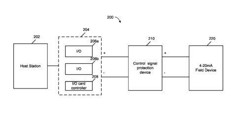
[0034] Fig. 2 is a schematic representation of a control system 200 in which a
control
signal protection device may be utilized to sustain a control signal in case
an interruption in
the control signal occurs. The control system 200 includes a host station 202
connected to a
redundant I/0 subsystem 204. Referring to Fig. 1, in an embodiment, the host
station 202
corresponds to the host station 111a or the host station 111b, and the I/0
subsystem 204 is
included in the I/0 card bank 116, for example. The output of the I/0
subsystem 204 is
provided to a field device 220 for controlling operation of the field device
220. The field
device 220 may be a suitable 4-20mA field device, such as a current to
pressure transducer or
a valve controller, for example, that may accept a control signal in the 4 to
20 mA range and
convert the control signal to a pneumatic control signal for controlling the
position of a valve.
[0035] The I/0 subsystem 204 includes a redundant configuration that provides
redundant
control for the field device 220. In particular, the I/O subsystem includes a
first I/0 card
206a and a second I/0 card 206b. The VO card 206a may be a primary or active
I/0 card,
while the I/0 card 206b may be a back-up I/0 card. An I/0 card controller 208
may control
the operation of the I/0 subsystem 204 by automatically switching operation
from the
primary card 206a to the backup card 206b in an event of failure of the
primary card 206a.
Additionally, the I/0 controller 208 may be configured to switch operation
from the primary
card 206a to the back-up card 206b periodically in order to verify
functionality of the back-up
card 206b. Switchover from the primary card 206a to the back-up card 206b, or
from the
back-up card 206b back to the primary card 206a, in general, may cause an
interruption in the
control signal present at the output of the I/0 subsystem 204. Such
interruption in control
signal provided to the field device 220 may cause certain undesired effects in
the process
being controlled. For example, temporary loss of control signal provided to a
valve controller
may cause the corresponding valve to move to an unintended position, thereby
potentially
disrupting normal operation of the process being controlled. Further, in some
situations,
temporary loss of a control signal may cause a valve controller to cause the
valve to latch in a
safe state, such as in a fully opened or in a fully closed position, for
example, or in another
predetermined position. For example, the valve controller may be associated
with an
emergency shutdown valve that, in response to a loss in a control signal, may
cause the
emergency shutdown valve to latch in a fully closed position to prevent flow
of a liquid, for
example. In such situations, return to normal operation of the valve may
require an operator
to manually unlatch the valve.
- 8 -
CA 02880402 2015-01-27
WO 2014/028472 PCT/US2013/054706
[0036] The system 200 includes a control signal protection device 210
connected in series
with the I/0 subsystem 204 and the field device 220. As illustrated in Fig. 2,
the control
signal protection device 210 includes a pair of input terminals 212 and a pair
of output
terminals 214. The input terminals 212 connect the control signal protection
device 210 to a
current loop (e.g., 4-20mA current loop) that provides control signals from
the I/0 subsystem
204 to the field device 220. The output terminals 214 connect the control
signal protection
device 210 to control signal current loop terminals of the field device 220.
Generally
speaking, the control signal protection device 210 is configured to sustain a
signal level (e.g.,
a voltage level) at the output terminals 214 of the control signal protection
device 210 for a
certain period of time in an event of a loss or temporary interruption of
control signal at the
input terminals to the control signal protection device 210. To this end. the
control signal
protection device 210 may include or be coupled to a storage element (e.g., a
capacitor) that
may store sufficient amount of energy in the storage element during normal
operation of the
control system 200 and may then utilize the stored energy to sustain the
control signal at the
output of the device 210 for the duration of a temporary interruption of the
control signal at
the input to the device 210. As a result, operation of the field device 220
will not be affected
by a temporary control signal loss, such as during a switchover operation
between the
primary card 206a and the backup card 206b. As an example, a control signal
provided to a
valve via the control signal protection device 210 will be maintained at a
sufficient level
above a shutdown threshold of the valve being controlled, and, as a result,
the valve will not
shut down and will need to be reset in the event of a temporary control signal
interruption, in
an embodiment.
[0037] In an embodiment, the control signal protection device 210 operates by
extracting a
small amount of power from the control signal loop (e.g., 4-20 m A control
signal loop) and
stores the extracted power in a storage element (e.g., a capacitor) included
in or coupled to
the signal protection device 210. In a normal mode of operation of the signal
protection
device 210, when control signal is present at the input of the control
protection device 210,
the signal protection device 210 presents a filtered version of the control
signal at the output
of the control protection device 210. Thus, in the normal mode of operation,
the control
signal device 210 generally passes the control signal from the host station
202 to the field
device 220 to control operation of the field device 220. In an embodiment, the
signal
protection device 210 is configured to pass the control signal from the host
station 202 to the
- 9 -
CA 02880402 2015-01-27
WO 2014/028472 PCT/US2013/054706
field device 220 without heavily filtering of the control signal and,
therefore, without a
significant delaying the control signal provided to the field device 220.
Further, in an
embodiment, the control signal protection device 210 is configured to extract
a sufficiently
small amount of power from the control current loop so as to not disturb
operation of the
current loop, and to not significantly interfere with communication signals
(e.g., HART
communication signal) on the current loop, during normal operation of the
control system
200.
[0038] The control signal protection device 210 is configured to monitor the
input current
(or voltage) at the input terminals 212 and to detect when the input current
(or voltage) at the
input terminals 212 falls below a certain threshold, indicating a loss of a
control signal from
the I/0 subsystem 204 at the input of the control signal protection device
210. In response to
detecting the loss of control signal at the input of the control signal
protection device 210, the
control signal protection device 210 is configured to switch operation to a
protection mode, in
which power stored in the storage element us utilized to sustain a control
signal level across
the output terminals 214 of the control signal protection device 210. The
control signal
protection device 210 is also configured to detect when the monitored input
current (or
voltage) at the input terminals 212 rises above the threshold, indicating that
the control signal
from the I/0 subsystem 204 has been reestablished. When detected that the
control signal has
returned at the input to the control signal protection device 210, the control
signal protection
device 210 is configured to switch operation to the normal mode of operation,
in which a
filtered version of the control signal present at the input terminals 212 of
the control signal
protection device 210 is transferred to the output terminals 214 of the
control signal
protection device 210.The control signal protection device 210 may be
integrated with the
field device 220. For example, the control signal protection device 210 may be
integrated
into a local control panel provided with a field device to manually operate
the field device,
such as to manually open or close a safety shutdown valve. As another example,
the control
signal protection device 210 may be integrated into a HART filter device
provided to
facilitate HART communication between the field device 220 and the host
station 202, for
example when the field device 220 is not configured for communication
according to the
HART communication protocol. Alternatively, the field device 210 may be
provided as an
external component that may connect serially with a control input to the field
device 220. In
some embodiments, the control signal protection device 210 may be a multi-
channel device
- 10 -
CA 02880402 2015-01-27
WO 2014/028472 PCT/US2013/054706
capable of providing control signal protection for multiple control inputs of
the field device
220 and/or for respective control inputs of multiple field devices.
[0039] The control signal device 210 may receive the control signal supplied
by the I/0
subsystem 204 via a wired connection with the I/0 subsystem 204, as
illustrated in Fig. 2, or
may receive the control signal from a control station wirelessly, for example
via a bank of
redundant wireless I/0 cards. With respect to Fig. 1, the field device 220
corresponds to a 4-
20mA or a HART field device 122, in one embodiment. In another embodiment, the
field
device 220 corresponds to a 4-20mA or a HART field device configured for
wireless
communication with a host station.
[0040] Fig. 3 is a diagram illustrating a circuit 300 corresponding to one
possible
implementation of the control signal protection device 210. The circuit 300
includes a pair of
input terminals 302 and a pair of output terminal 304. The input terminals 302
may be
communicatively coupled to an output of an I/0 card subsystem within a control
system. The
output terminals 304 may be connected to a field device, such as to a valve
controller, for
example. The circuit 300 operates by extracting or harvesting a small amount
of electric
energy generated by the current flowing through the circuit 300 and storing
this extracted
power in a power storing element within the circuit 300. This stored energy
may then be
used to maintain a desired voltage level across the output terminal pair 304
in an event of a
short interruption of the current entering the circuit 300 at the input
terminals 302, such as
due to a temporary control signal loss during an I/0 card switchover
operation. Alternatively,
circuits similar to the circuit 300 may operate by using the stored power to
supply a desired
current (rather than voltage) to the output terminals 304 during an
interruption in input
current to the circuit 300.
[0041] The circuit 300 may include a first switch 308 and a second switch 312.
Each of
the switches 308 and 312 may be a Metal Oxide Semiconductor Field Effect
Transistor
(MOSFET), a different type of a transistor, or any other electronic switching
means known in
the art. A first operational amplifier ("op amp") 306 may be provided to
control the
operating state of the switch 308, and a second operational amplifier 310 may
be provided to
control the operating state of the second switch 312. It will be appreciated
that discrete
transistors may be used as control elements for controlling the operation of
the switches 306
and 308 in place of the op amps 306 and 310, in some embodiments.
- 11 -
CA 02880402 2015-01-27
WO 2014/028472 PCT/1JS2013/054706
[0042] When current entering the circuit 300 is sufficiently high (e.g.,
greater than 2mA),
the circuit 300 may operate in a normal operational mode by supplying the
current to the
output terminals 304. In the normal operational mode, the output of the op amp
306 is
sufficiently high to keep the switch 308 in an open state. Consequently, the
inputs to the op
amp 310 may be such that the op amp 310 operates in a saturated state. As
illustrated, the
output of the op amp 310 is used to control the state of the switch 312 and
the saturated state
of the op amp 310 maintains the switch 312 in an open state.
[0043] With continued reference to Fig. 3, a capacitor 314 and a capacitor 316
are
provided to store power during normal operational mode of the circuit 300 for
sustaining
output voltage across the output terminals 304 for the duration of a temporary
interruption of
the control signal provided to the circuit 300. In order to store power in the
capacitors 314
and 316 during normal operational mode of the circuit 300 at a sufficiently
low rate as to not
interfere with the normal operation of the circuit 300, for example to
maintain a sufficiently
low delay introduced by the circuit 300, or to not interfere with normal
communication (e.g.,
HART communication) on the loop, the rate of storage of energy in the
capacitors 314. 316 is
controlled by resistors 320 and 318, respectively. As an alternative to the
two capacitor
configuration used for power storage as illustrated in Fig. 3, in some
embodiments, a single
capacitor may be used as the power storing element in the circuit 300.
Alternatively, other
methods of storing power may be utilized. For example, a charge pump or an
inductive boost
circuit may be provided. In such embodiments, power may be stored at a higher
voltage level
across the output terminals 304 compared to the voltage level across the input
terminals 302
of the circuit 300.
[0044] The current entering the circuit 300 may be monitored by a current
monitoring
circuit for the purpose of controlling the operational mode of the circuit
300. In the
embodiment of Fig. 3, the current monitoring circuit comprises a combination
of resistors
340, 342 and 344 along with a capacitor 346 coupled across the input terminals
of the op amp
306. When the input current entering the circuit 300 falls below a certain
threshold (e.g.,
below 2mA) the current monitoring circuit causes the circuit 300 to switch
operation from the
normal operational mode of the circuit 300 to a protection operational mode of
the circuit
300. In the protection operational mode, the voltage at the output terminals
304 of the circuit
300 is sustained at a desired level for the duration of the interruption of
current entering the
circuit 300. Because very little or no current enters the circuit 300, in this
operational mode,
- 12-
CA 02880402 2015-01-27
WO 2014/028472 PCT/US2013/054706
the voltage difference across the input terminal of the op amp 306 becomes
sufficiently small
such that the output of the op amp 306 controls switch 308 to transition to a
closed state.
Closed state of the switch 308, in turn, results in an increase in the voltage
level at the
negative terminal of the op amp 310 and, accordingly, causes a decrease in a
voltage
differential across the input terminals of the op amp 310. As a result, the
voltage level at the
output terminal of the op amp 310 drops, causing the switch 312 to transition
to a closed
state. In the closed state, the switch 312 effectively connects the negative
terminal of the
capacitor 314 with the positive terminal of the capacitor 316, and the energy
stored in the
capacitors 314 and 316 is supplied to the positive side of the output terminal
pair 304.
[0045] The voltage level maintained across the output terminals 304 of the
circuit 300 in
the protection operational mode of the circuit 300 is determined by a voltage
maintaining
element included in the circuit 300, such as a voltage divider formed by a
resistor 322 and a
resistor 324. Further, capacitor 326 is filters the voltage presented across
the output terminals
304. Thus, when the circuit 300 transitions from the normal operational mode
to the
protection operational mode, the voltage across the output terminals 304 of
the circuit 300 is
sustained at a scaled and filtered voltage level at the positive terminal of
the capacitor 326.
Accordingly, the voltage drop across the output terminal 304 corresponds to
the voltage level
across the terminals 304 prior to the input current interruption (i.e., in the
normal operational
mode). As a result, voltage across the output terminals 304 does not
experience a significant
change during a control signal interruption at the input terminals 302 of the
circuit 300. .
[0046] Subsequently, when control signal is returned to the circuit 300, such
as upon
completion of switchover from the primary card 1/0 card 206a to the back-up
I/0 card 206b
in the I/0 subsystem 204 (Fig. 2), electric current at the input terminals 302
of the circuit 300
increases and crosses the threshold value determined by the current monitoring
element of the
circuit 300. When input current is above the threshold level (e.g., above
2mA), op amps 306
and 310 control respective switches 308 and 312 to transition to an open
state. Accordingly,
in this case, the circuit 300 returns to the normal operational mode.
[0047] In some embodiments, the circuit 300 includes additional components to
improve
performance of the circuit 300 and/or increase robustness of the circuit 300
in presence of
transient noise or interference in the circuit 300. For example, the
implementation of the
circuit 300 illustrated in Fig. 3 includes zener diodes 328, 330 connected
across the input
terminals 302 and across the output terminals 304, respectively, of the
circuit 300. The zener
- 13 -
CA 02880402 2015-01-27
WO 2014/028472 PCT/US2013/054706
diodes 328, 330 are provided for protection of the circuit 300 against
transient interference at
the input and the output of the circuit 300. A capacitor 332 may be provided
to filter the
voltage supplied to the op amps 306 and 310 to improve performance of the op
amps 306 and
310. Further, a zener diode 334 and a resistor 338 may be used to supply
desired voltage
limited power to the op amps 306 and 310. To this end, the zener diode 334 and
the resistor
338 may be selected in accordance with the maximum voltage specified for the
particular op
amps 306 and 310 being utilized. It should be noted that such additional
components may
not necessary for proper operation of the circuit 300 and at least some of the
additional
components are omitted from the circuit 300 in some implementations.
[0048] While the present invention has been described with reference to
specific examples,
which are intended to be illustrative only and not to be limiting of the
invention, it will be
apparent to those of ordinary skill in the art that changes, additions and/or
deletions may be
made to the disclosed embodiments without departing from the spirit and scope
of the
invention.
- 14-