Note: Descriptions are shown in the official language in which they were submitted.
CA 02880769 2015-02-02
DESCRIPTION
PUMP PROBE MEASURING DEVICE
Technical Field
[0001] The present invention relates to a pump probe measuring
device.
Background Art
[0002] To measure ultrafast phenomena that occur in picosecond (ps)
to femtosecond (fs) regions, measurements using an ultrashort pulse
laser are carried out widely. For example, in a pump probe reflectance
measurement, a high-intensity pump pulse is focused to an object to
be measured first to excite the sample instantaneously. Then, while
the excited state is being relaxed, an irradiation of a low-intensity
probe pulse is applied, and the intensity of the reflected light is
measured. The measured intensity of the reflected light is
proportional to the reflectance of the sample at the moment when it is
hit by the probe pulse. By measuring the intensity of the reflected
light while gradually changing the delay time of the probe pulse with
respect to the pump pulse, change in the reflectance of the sample
between before and after the excitation can be observed with the time
resolution comparable to the duration of the laser pulse. This time
resolution falls within a picosecond to femtosecond range.
[00031 Since the intensity of signals obtained by such ultrahigh-speed
measurement is extremely weak in many cases, a modulation
measurement is performed to improve the signal-to-noise ratio. As the
most common method, the intensity of the pump pulse is modulated,
and the response of the probe signal to this modulation is detected by
using a lock-in amplifier. In addition, methods in which polarization
of the light of the pump pulse or the delay time is modulated are also
known.
[0004] It is especially noteworthy that the delay time modulation
method, in which delay time is modulated as a rectangular wave, has
recently been found to be effective in order to realize a time-resolved
scanning probe microscope, which is a scanning probe microscope
¨1¨
CA 02880769 2015-02-02
combined with a pulse laser. The time-resolved scanning probe
microscope achieving 1-ps temporal resolution and 1-nm spatial
resolution at the same time has thus been constructed.
[0005] To control the delay time of laser pulse precisely in a time
domain from fs to nanosecond (ns), the length of optical path is
generally varied.
[0006] FIG. 10 is a view illustrating the configuration of a
conventional delay time modulation device. As shown in FIG. 10, the
conventional delay time modulation device performs a periodic delay
time modulation by mechanically vibrating the position of mirror. The
laser pulse from the light source is divided by a half mirror 1 (HM1)
into two optical paths, namely a path to a retroreflector 1 (RR1) and
that to a retroreflector 2 (RR2). It is not necessary that the amount of
light at dividing is 1:1. Any ratio can be selected arbitrarily
depending on the property of the half mirror to be used. RR1 and RR2
are devices that reflect optical pulses in a direction directly opposite
to the incident direction. Retroreflectors usually composed of three
mirrors placed so that they make right angles to one another are
generally used. The reflected lights from RR1 and RR2 are overlapped
precisely on the same optical axis at a half mirror 2 (HM2).
[0007] When the length of the optical path passing through RR1
differs from that of the optical path passing through RR2, optical
pulses appear at different positions temporally deviated from each
other on the optical axis overlapped at 11M2. The delay time between
the two pulses can be controlled precisely by mechanically varying the
position of RR1 or RR2. By using a piezoelectric device, etc., the
accuracy of 1 fs or shorter can be achieved. To modulate the delay
time periodically using such a device, it is only necessary to
periodically change the position of RR1, for example. So far, many
measurements have been carried out wherein the mirror position is
varied periodically to perform the delay time modulation as described
above.
[0008] However, the device as shown in FIG. 10 has major limitations
in the amplitude of modulation and in the frequency of modulation.
The optical path length and the delay time are proportional to each
other, with the velocity of light serving as the coefficient. For example,
¨2¨
CA 02880769 2015-02-02
the position of the mirror must be varied with the amplitude of 1.5 cm
to modulate the delay time by 100 ps. Such a significant modulation
in the mirror position can be achieved only at an extremely low
frequency of approximately 10 Hz. In using an amplitude about 1.5 cm
or more, or a frequency about 10 Hz, problems may arise. The
mechanical vibration may be generated and give bad influences to the
optical device located around. It becomes impossible to realize the
accurate modulation due to the deformation of the driving mechanism
itself.
[0009] Meanwhile, since the result of the modulation performed at
such a low frequency is strongly affected by the fluctuation in the
intensity of laser light, etc., the time-resolved measurement with
modulating mirror position is only useful when the modulation
amplitude is very small (of up to about 100 fs).
[0010] Recently, following the development of a time-resolved
scanning probe microscope, which is a scanning probe microscope
adopting delay time modulation of a pulse laser, a delay time
modulation method using high speed optical shutters (called pulse
pickers) capable of passing or blocking optical pulses with respect to
each pulse has been proposed, and its usefulness has been confirmed
(Patent Literature 1).
[0011] FIG. 11 is a time chart illustrating the conventional delay time
modulation method using pulse pickers.
A laser oscillator generates laser pulses at time intervals of
approximately 10 ns, and these laser pulses are split into two optical
paths by a half mirror, etc., and are introduced to respective two
pulse pickers from the right-hand side. The pulse picker can
selectively transmit one optical pulse at arbitrary timing from the
continuous pulse train.
[0012] It is therefore possible, as shown in FIG. 11, to generate a
delay time by transmitting pulses at different timing. When the delay
time is generated by using pulse pickers as described above, the delay
time modulation can be performed at extremely high speed and with
large amplitude. In the first place, with this method, the minimum
value of the amplitude of the modulation delay time is determined by
the pulse interval of the optical pulse train, and typically it is
¨3¨
CA 02880769 2015-02-02
approximately 10 ns. This value is equivalent to approximately 3 m in
the length of optical path, which is 3 to 4 orders greater than that of
the amplitude of the delay time modulation achievable by changing
mirror positions. Furthermore, the delay time can be changed for each
transmission pulse with this method. Thus, approximately 1 MHz
high-speed modulation can be performed as required.
[0013] Meanwhile, the delay time modulation using pulse pickers as
shown in FIG. 11 cannot produce favorable results when applied to
observing fast phenomena of 1 ns or faster. This is because that
pulses are picked to generate delay time, thus causing the excitation
frequency of the sample, namely the number of times of measurement
per unit time, to decrease significantly.
[0014] When water-cooled type Pockels cells are used as pulse pickers,
for example, it is difficult to increase the repetition frequency of the
output optical pulses to higher than 2 MHz due to the restriction
imposed by the generation of heat from the Pockels cells. Whereas the
repetition frequency of the conventional titanium-sapphire laser
oscillator is generally close to 100 MHz, the number of times of
excitation of the sample per unit time becomes 1/50, and also the
number of detected signals becomes 1/50, when pulse pickers are used.
Citation List
Patent Literature
[0015] Patent Literature 1: JP 2008-139029 A
Non-Patent Literature
[0016] Y. Terada, S. Yoshida, 0. Takeuchi and H. Shigekawa, "Real
space imaging of carrier dynamics by nanoscale pump-probe
microscopy", Nature Photonics DOI:10.1038/NPHOTON.2010.235
(2010)
Summary of Invention
Technical Problem
[0017] The problem of the conventional pump probe measuring device
is that the high-sensitivity measurement cannot be performed when it
is used to measure fast phenomena.
¨4¨
CA 02880769 2015-02-02
[0018] In consideration of the problem described above, an object of
the present invention is to provide a pump probe measuring device
capable of measuring fast phenomena of 1 ns or faster with high
accuracy.
Solution to Problem
[0019] To solve the above problem, the present invention provides a
pump probe measuring device including: an ultrashort optical pulse
laser generator for generating a first ultrashort optical pulse train
which is a pump light, a second ultrashort optical pulse train, which
has a first delay time with respect to the pump light and is a probe
light, and a third ultrashort optical pulse train, which has a second
delay time with respect to the pump light and is a probe light; an
optical shutter unit to which the second and the third ultrashort
optical pulse trains are introduced; an optical shutter control unit for
controlling the optical shutter unit; an irradiation optical system for
irradiating a sample with the pump light and the probe lights; and a
detecting unit including a sensor for detecting probe signals from the
sample and a phase-sensitive detecting means connected to the sensor,
wherein the second ultrashort optical pulse train and the third
ultrashort optical pulse train illuminate the sample alternately as the
probe light, controlled by the optical shutter control unit, to modulate
the delay times of the probe lights with respect to the pump light
periodically, thereby detecting the probe signals by the
phase-sensitive detecting means with synchronized to the periodic
modulation of the delay time.
[0020] In the above configuration, the ultrashort optical pulse laser
generator may include: an ultrashort optical pulse laser light source;
an optical element that divides an ultrashort optical pulse generated
by this ultrashort optical pulse laser light source into three to form a
first ultrashort optical pulse train which is the pump light, and
second and third ultrashort optical pulse trains which are the probe
lights; a first optical delay unit for delaying the second ultrashort
optical pulse train with respect to the pump light by a first delay
time; and a second optical delay unit for delaying the third ultrashort
optical pulse train with respect to the pump light by a second delay
¨5¨
CA 02880769 2015-02-02
time.
The ultrashort optical pulse laser generator may also include:
a first ultrashort optical pulse laser light source for generating the
pump light; a second ultrashort optical pulse laser light source for
generating a second ultrashort optical pulse train which is the probe
light; and a third ultrashort optical pulse laser light source for
generating a third ultrashort optical pulse train which is the probe
light, wherein the first to the third ultrashort optical pulse laser light
sources may oscillate synchronously with specified delay times.
The optical shutter unit includes: a first optical shutter; and a
second optical shutter, wherein the second ultrashort optical pulse
train may be introduced to the first optical shutter, and the third
ultrashort optical pulse train may be introduced to the second optical
shutter.
The optical shutter unit may include only one optical shutter
that has an electrooptic element and a polarization rotation element,
wherein the second and the third ultrashort optical pulse trains may
be introduced to the optical shutter unit.
The pump probe measuring device may further include: a first
optical delay unit for delaying the second ultrashort optical pulse
train with respect to the pump light by the first delay time; and a
second optical delay unit for delaying the third ultrashort optical
pulse train with respect to the pump light by the second delay time.
The sensor may be comprised of a photodiode, and a reflected
light of the probe light at the sample may be introduced to the
photodiode, and an intensity of the reflected light may be detected as
a first probe signal.
The sensor may be comprised of a scanning probe microscope,
and a second probe signal may be detected by a probe of the scanning
probe microscope on a surface of the sample, to which the pump light
and the probe lights are focused.
[0021] A measuring device according to the present invention includes
any one of the above-mentioned pump probe measuring devices.
Advantageous Effects of Invention
[0022] According to the present invention, in a time-resolved
¨6¨
CA 02880769 2015-02-02
measurement using a pulse laser covering a femtosecond region, faint
signals can be measured highly sensitively, accurately, and stably in
a wide measurement range including phenomena having short to long
relaxation time, without modulating the intensity of illuminating
light or picking pulses using pulse pickers. According to the present
invention, a pump probe measuring device for measuring and
analyzing ultrafast physical phenomena on the order of ps, 1 ns or
faster for example, can be provided along with a time-resolved
scanning probe microscope using this measuring device.
Brief Description of Drawings
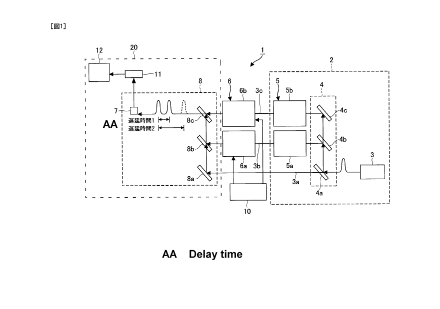
[0023] FIG. 1 is a view illustrating a typical configuration of a pump
probe measuring device according to a first embodiment of the present
invention.
FIG. 2 is a time chart illustrating the relation among a pump
light, a first probe light, a second probe light, the pump light plus the
first probe light illuminating the sample, and the pump light plus the
second probe light illuminating the sample.
FIG. 3 is a time chart illustrating the time change in delay
time.
FIG. 4 is a time chart illustrating the signal measured by the
detecting unit, namely the probe signal (P).
FIG. 5 is a chart illustrating the dependency of the probe
signal (P) on delay time Td.
FIG. 6 is a view illustrating a typical configuration of a pump
probe measuring device according to a second embodiment of the
present invention.
FIG. 7 is a view illustrating a typical configuration of a pump
probe measuring device according to a third embodiment of the
present invention.
FIG. 8 is a schematic view illustrating a detection unit using a
scanning tunnel microscope as a scanning probe microscope.
FIG. 9 is a chart showing the probe signal from the reflected
light of low-temperature-grown GaAs measured by the pump probe
measuring device.
FIG. 10 is a view illustrating the configuration of a
¨7¨
CA 02880769 2015-02-02
conventional delay time modulation device.
FIG. 11 is a time chart describing conventional pulse pickers.
Reference Signs List
[00241
1, 30, 40: Pump probe measuring device
2, 2A: Ultrashort optical pulse laser generator
3: Laser light source
3a: Pump light
3b: First probe light
3c: Second probe light
4: Branch optical system
4a to 4d: Mirror
4b, 4c, 4g: Half mirror
5: Optical delay unit
6, 6A: Optical shutter unit
6a, 6b, 6c: Pockels cell
6d: Mirror
6e: Half mirror
7: Sample
8, 8A: Irradiation optical system
8a: Mirror
8b, 8c: Half mirror
10: Optical shutter control unit
11: Sensor
12: Phase-sensitive detecting means
15: Probe
16: DC power supply
17: Current meter
20: Detecting unit
31: Polarization rotation element (1/2 X plate)
43: Laser light source
Description of Embodiments
[0025] The embodiments of the present invention will hereinafter be
described in detail by referring to drawings.
¨8¨
CA 02880769 2015-02-02
(First Embodiment)
FIG. 1 is a view illustrating a typical configuration of a pump
probe measuring device 1 according to the first embodiment of the
present invention. As shown in FIG. 1, the pump probe measuring
device 1 includes: an ultrashort optical pulse laser generator 2 for
generating a first ultrashort optical pulse train which is a pump light
3a, a second ultrashort optical pulse train, which is a first probe light
3b, and a third ultrashort optical pulse train which is a second probe
light 3c; an optical shutter unit 6 to which the second and the third
ultrashort optical pulse trains are introduced; an optical shutter
control unit 10 for controlling the optical shutter unit 6; an
irradiation optical system 8 for directing the pump light 3a and the
probe lights 3b, 3c to a sample; and a detecting unit 20 including a
sensor 11 for detecting a probe signal from the sample 7 and a
phase-sensitive detecting means 12 for detecting the probe signal.
[0026] The ultrashort optical pulse laser generator 2 generates the
first ultrashort optical pulse train which is the pump light 3a, the
second ultrashort optical pulse train, which has a first delay time
with respect to the pump light 3a and is the first probe light 3b, and
the third ultrashort optical pulse train, which has a second delay time
with respect to the pump light and is the second probe light 3c.
[0027] The ultrashort optical pulse laser generator 2 includes: a laser
light source 3; a branch optical system 4; and an optical delay unit 5.
The branch optical system 4, which is comprised of optical elements,
branches the laser light from the laser light source 3 into the pump
light 3a, the first probe light 3b, and the second probe light 3c.
[0028] The laser light source 3 is a femtosecond pulse laser light
source, for example. Specifically, a titanium-sapphire laser oscillator
can be used as the laser light source, which generates laser pulses
having wavelength of approximately 800 nm and time width of
approximately 25 fs at repetition frequency of approximately 100 MHz,
and average brightness of approximately 1W.
[0029] The branch optical system 4 includes: a first half mirror 4a to
which the light from the laser light source 3 is introduced; a second
half mirror 4b, which is installed on the optical path of the reflected
light from the first half mirror 4a; and a first mirror 4c, which is
¨9¨
CA 02880769 2015-02-02
installed on the optical path of the light penetrating the second half
mirror 4b.
[0030] The second half mirror 4b is placed above the first half mirror
4a. The first mirror 4c is placed above the second half mirror 4b.
[0031] In the branch optical system 4, the laser pulse from the laser
light source 3 is branched into a transmitted light and a reflected
light by the first half mirror 4a placed on the optical path of the laser
pulse emitted from the laser light source 3. Here, the transmitted
light from the half mirror 4a is used as the pump light 3a, whereas
the reflected light is used as the first and the second probe lights 3b,
3c.
[0032] The second half mirror 4b, which is placed on the optical path
of the reflected light from the first half mirror 4a, branches this
reflected light into a transmitted light and a reflected light, allowing
the reflected light to serve as a second ultrashort optical pulse train,
and the transmitted light as a third ultrashort optical pulse train.
[0033] The optical delay unit 5 includes: a first optical delay unit 5a
to which the second ultrashort optical pulse train reflected by the
second half mirror 4b is introduced; and a second optical delay unit 5b
to which the third ultrashort optical pulse train penetrating the
second half mirror 4b and then reflected by the first mirror 4c is
introduced. The first and the second optical delay units 5a, 5b can be
configured using an optical system of publicly known structure that
adjusts optical path length using movable mirrors. For example, the
movable mirrors are a pair of reflecting mirrors placed obliquely at an
angle of 45 degrees with the incident light axis. The light entering
along the incident light axis is reflected by one of the reflecting
mirrors in a direction perpendicular to the incident light axis,
introduced to the other reflecting mirror, and reflected by that
reflecting mirror in a direction parallel to the incident direction.
[0034] The movable mirrors are thus moved in the direction of the
optical axis for adjustment, allowing the length of the optical path to
be adjusted. Accordingly, by moving the movable mirrors, the first
optical delay unit 5a emits the first probe light 3b having a first delay
time with respect to the first ultrashort optical pulse train which is
the pump light 3a, to the optical shutter unit 6. Generally, the
¨10¨
' CA 02880769 2015-02-02
movable range of the optical path length of movable mirrors is
approximately 30 cm, which provides delay time setting range of 0 to
1 ns between the pump light 3a and the first probe light 3b.
[0035] Similarly, with the second optical delay unit 5b, the second
delay time of the second probe light 3c with respect to the pump light
3a can be set by moving the movable mirrors.
[0036] As described above, the ultrashort optical pulse laser generator
2 generates, from the laser light emitted from the laser light source 3,
the first ultrashort optical pulse train which is the pump light 3a; the
second ultrashort optical pulse train, which has delay time Tdi with
respect to the pump light 3a and is the first probe light 3b; and the
third ultrashort optical pulse train, which has delay time Td2 with
respect to the pump light 3a and is the second probe light 3c.
[0037] The optical shutter unit 6 includes: a first optical shutter 6a to
which the second ultrashort optical pulse train, which is the first
probe light 3b, is introduced; and a second optical shutter 6b to which
the third ultrashort optical pulse train, which is the second probe
light 3c, is introduced. The optical shutter unit 6 is controlled by the
optical shutter control unit 10. A delay time modulation is performed
by opening the optical shutters 6a, 6b alternately. As the first and the
second optical shutters 6a, 6b, an acoustooptic modulator (AOM) or an
electrooptic modulator (EOM) can be used. As the electrooptic
modulator, Pockels cells can be used. By using Pockels cells as the
first and the second optical shutters 6a, 6b, a high-speed modulation
of 1 kHz or higher i.e. high frequency modulation can be performed
without involving a mechanical vibration, etc.
[0038] The optical shutter control unit 10 includes a function
generator and an inverter, for example. The function generator
generates a 1 kHz rectangular wave signal, and the output is sent to
the first optical shutter 6a. The inverter reverses the sign of the
signal from the functional generator, and the output is sent to the
second optical shutter 6b. This configuration allows the first optical
shutter 6a and the second optical shutter 6b to be opened alternately
at intervals corresponding to 1 kHz frequency, for example.
[0039] The detecting unit 20 includes: an irradiation optical system 8;
a sensor 11 for measuring probe signals obtained from reflected lights,
¨11¨
CA 02880769 2015-02-02
etc. of the probe pulse lights 3b, 3c illuminating the sample 7; and a
phase-sensitive detecting means 12 for detecting the dependency of
the probe signals on delay times.
The irradiation optical system 8 has the function of focusing
the pump light 3a generated from the ultrashort optical pulse laser
generator 2, the first probe light 3b having the first delay time with
respect to the pump light 3a, and the second probe light 3c having the
second delay time with respect to the pump light 3a, on the sample 7.
The irradiation optical system 8 as shown in FIG. 1 includes a second
mirror 8a and two half mirrors 8b, 8c. The irradiation optical system
8 may further include a mirror or an objective lens for guiding the
pump light 3a, the first probe light 3b, and the second probe light 3c
to the surface of the sample 7, respectively. The pump light 3a, the
first probe light 3b, and the second probe light 3c can thus be focused
on the surface of the sample 7.
[0040] When the intensity of the reflected light is measured as the
probe signal, the sensor 11 may be configured using a Si photodiode,
for example. As the photodiode, a pin photodiode can be used. The
probe light reflected by the sample 7 is introduced to the pin
photodiode, and the intensity of the obtained reflected light can be
measured as the probe signal.
[0041] As the phase-sensitive detecting means 12, a dual-phase
lock-in amplifier can be used. By inputting the probe signal into the
dual-phase lock-in amplifier, and performing a phase-sensitive
detection at the delay time modulation frequency in the shutter
control unit 10, the dependency of the probe signal from the sample 7
on the delay time can be measured by the sensor 11.
[0042] First, the optical path of the pump light 3a from the laser light
source 3 to the sample 7 will be described.
The light from the laser light source 3 penetrates the first half
mirror 4a, is reflected by the second mirror 8a, and then penetrates
the third half mirror 8b. This transmitted light is reflected by the
fourth half mirror 8c and is the pump light 3a to be introduced to the
sample 7.
[0043] The first probe light 3b from the laser light source 3 to the
sample 7 will then be described.
¨12¨
CA 02880769 2015-02-02
The light reflected by the first half mirror 4a, of the light
coming from the laser light source 3, is divided into a transmitted
light and a reflected light by the second half mirror 4b. On the optical
path of this reflected light, the first optical delay unit 5a, the first
optical shutter 6a, and the third half mirror 8b are placed.
Consequently, the light reflected by the first half mirror 4a
and then by the second half mirror 4h, of the light from the laser light
source 3, passes through the first optical delay unit 5a and the first
optical shutter 6a, is reflected by the third half mirror 8b and then by
the fourth half mirror 8c, and is the first probe light 3b, which is
guided to the sample 7. The first optical delay unit 5a causes a delay
time LH to occur to the first probe light 3b, which is thus allowed to
reach the sample 7 when Tai has elapsed since the pump light 3a
reaches.
[0044] The second probe light 3c from the laser light source 3 to the
sample 7 will then be described.
The light having penetrated the second half mirror 4b, of the
light from the laser light source 3, is reflected by the first mirror 4c.
On the optical path of this reflected light, the second optical delay
unit 5b, the second optical shutter 6b, and the fourth half mirror 8c
are placed.
Consequently, the light that is reflected by the first half
mirror 4a and then penetrates the second half mirror 4b, of the light
from the laser light source 3, is reflected by the first mirror 4c,
penetrates the second optical delay unit 5b and the second optical
shutter 6b, penetrates the fourth half mirror 8c, and then is guided to
the sample 7 as the second probe light 3c. The second optical delay
unit 5b causes a delay time Td2 to occur to the second probe light 3c,
which is thus allowed to reach the sample 7 when Td2 has elapsed
since the pump light 3a reaches.
[0045] FIG. 2 is a time chart illustrating the relation among the pump
light 3a, the first probe light 3b, the second probe light 3c, the pump
light 3a and the first probe light 3b impinging on the sample 7, and
the pump light 3a and the second probe light 3c impinging on the
sample 7.
The horizontal axis in FIG. 2 represents time. The vertical
-13-
CA 02880769 2015-02-02
axis represents, from top to bottom, the intensity of the pump light
3a; that of the first probe light 3b, that of the second probe light 3c;
that of the incident light (delay time: Tap illuminating the sample 7
when the first probe light 3b only is made to pass by the optical
shutter unit 6; and that of the incident light (delay time: Td2)
illuminating the sample 7 when the second probe light 3c only is made
to pass by the optical shutter unit 6.
As shown in FIG. 2, the optical shutter unit 6 allows either
the first probe light 3b or the second probe light 3c only to be
introduced to the sample 7. Consequently, the incident light to the
sample 7 consists of a pulse pair having the delay time Tdi when the
first probe light 3b is introduced, and a pulse pair having the delay
time Td2 when the second probe light 3c is introduced.
[0046] FIG. 3 is a time chart illustrating the time change in delay
time (Td). As shown in FIG. 3, by switching the optical shutter unit 6
periodically, the delay time of the probe light is modulated between
Tdi and Td2, following the form of a rectangular wave.
[0047] FIG. 4 is a time chart illustrating the temporal change of the
probe signal (P) measured by the sensor 11. As shown in FIG. 4, the
probe signal measured by the sensor 11 in accordance with a periodic
modulation of the delay time is in a form of a rectangular wave signal
vibrating between P(Tdi) and P(Td2).
[0048] As a result of the probe signal vibrating in a form of a
rectangular wave being input to the phase-sensitive detecting means
12, the measurement value obtained by the phase-sensitive detecting
means 12 is proportional to the difference between probe signals
P(Tdi) and P(Td2) that correspond to the delay time of Tdi and Td2,
respectively, namely P(Tdi)¨P(Td2).
FIG. 5 is a chart showing the dependency of the probe signal
(P) on delay time Td. As shown in FIG. 5, since the dependency of the
probe signal on delay time P(Td) for large Td value, generally becomes
asymptotic to the equilibrium value of P, namely P(00), especially
when a large delay time Td2 is adopted, the measurement value can be
regarded approximately as P(Td1)¨P(00). In this case, the measurement
value becomes proportional to P(Tdi) itself, which is the value
measured with reference to P(0).
¨14¨
CA 02880769 2015-02-02
By using the pump probe measuring device 1 of the present
invention, the dependency of the probe signal on delay time can thus
be measured highly accurately for ultrafast phenomena of 1 ns or
faster, namely on the order of ps.
[0049] The typical pulse repetition frequency, the pulse repetition
period, 2 delay times, and the delay time modulation frequency are
shown below.
Pulse repetition frequency: 100 MHz
Pulse repetition period: 10 ns
2 delay times: 0 to 5 ns
Delay time modulation frequency (opening/closing
frequency of the shutter): I kHz (period: 1 ms)
[0050] (Second Embodiment)
FIG. 6 is a schematic view illustrating the configuration of a
pump probe measuring device 30 according to a second embodiment of
the present invention. As shown in FIG. 6, the pump probe measuring
device 30 according to the second embodiment of the present
invention differs from the pump probe measuring device I according
to the first embodiment in that an optical shutter unit 6A is provided
instead of the optical shutter unit 6 as shown in FIG. 1. The optical
shutter unit 6A includes: a Pockels cell, which functions as an optical
shutter 6c; a fifth half mirror 6e; a polarization rotation element 31;
and a third mirror 6d. The irradiation optical system 8A includes the
second mirror 8a and the third half mirror 8b. In other words, the
number of half mirrors used in the irradiation optical system 8A in
this embodiment is one less than that of the irradiation optical
system 8 as shown in FIG. I. The optical shutter control unit 10 has a
circuit for generating 1 kHz rectangular wave, for example, as the
signal for controlling the Pockels cell, which functions as the optical
shutter 6c. As the optical shutter control unit 10, a pulse generator or
the function generator can be used. The following description of FIG.
6 assumes that the optical shutter 6c is the Pockels cell.
[0051] First, the optical path of the pump light 3a from the laser light
source 3 to the sample 7, will be described. The light from the laser
light source 3 penetrates the first half mirror 4a, is reflected by the
second mirror 8a, and then by the third half mirror 8b, and is the
¨15¨
CA 02880769 2015-02-02
pump light 3a that is to be introduced to the sample 7.
[0052] The optical path of the first probe light 3b from the laser light
source 3 to the sample 7, will then be described. The light reflected by
the first half mirror 4a, of the light from the laser light source 3, is
divided into a transmitted light and a reflected light by the second
half mirror 4b. On the optical path of this reflected light, the first
optical delay unit 5a, the polarization rotation element 31, and the
third mirror 6d are placed. As the polarization rotation element 31, a
1/2 A plate can be used. The 1/2 A plate 31 is also called a half-wave
plate.
[0053] Accordingly, the light reflected by the first half mirror 4a, and
then by the second half mirror 4b, of the light from the laser light
source 3, penetrates the first optical delay unit 5a and the 1/2A plate
31, is reflected by the third mirror 6d, and then by the fifth half
mirror 6e, penetrates the Pockels cell 6c, and is introduced to the
sample 7 as the first probe light 3b. The delay time Tdi is generated to
this first probe light 3b by the first optical delay unit 5a. Thus, the
first probe light 3b reaches to the sample 7 when LH_ has elapsed
since the pump light 3a reaches to the sample 7.
[0054] Next, the optical path of the second probe light 3c from the
laser light source 3 to the sample 7 will be described.
The light having penetrated the second half mirror 4b, of the
light from the laser light source 3, is reflected by the first mirror 4c.
On the optical path of this reflected light, the second optical delay
unit 5b, the fifth half mirror 6e, the Pockels cell 6c, and the third half
mirror 8b are placed. Accordingly, the light having been reflected by
the first half mirror 4a and then having penetrated the second half
mirror 4b, of the light from the laser light source 3, is reflected by the
first mirror 4c, penetrates the second optical delay unit 5b, the fifth
half mirror 6e, the Pockels cell 6c, and the third half mirror 8b, and
then is introduced to the sample 7 as the second probe light 3c. The
delay time Td2 is generated to this second probe light 3c by the second
optical delay unit 5b. Thus, the second probe light 3c reaches the
sample 7 when Td2 has elapsed since the pump light 3a reaches the
specimen 7.
[0055] When the Pockels cell 6c does not allow a light having a certain
¨16¨
CA 02880769 2015-02-02
polarization direction to pass, namely when it blocks that light, the
light in the polarization direction, which is orthogonal to the direction
of the blocked light, penetrates the element with little loss.
Conversely, when the light having a certain polarization direction is
allowed to pass with little loss, the light in the direction orthogonal to
the direction of that light is blocked.
Hence, when the polarization direction of the second pulse
train and that of the third pulse train are made to cross orthogonal to
each other by placing the polarization rotation element 31 such as the
1/2 A plate, opening the Pockels cell 6c to the second pulse train
means that the Pockels cell 6c is automatically closed to block the
third pulse train. Conversely, closing the Pockels cell 6c to block the
second pulse train means that the Pockels cell 6c is automatically
opened to pass the third pulse train. In spite that the pump probe
measuring device 30 as shown in FIG. 6 has only one Pockels cell 6c
functioning as the optical shutter, unlike the pump probe measuring
device 1 as shown in FIG. 1, which requires two optical shutters 6a,
6b, the same operation as the pump probe measuring device 1 can be
ensured.
[0056] According to the pump probe measuring device 30, by placing
the 1/2 A plate 31 after one of the optical delay unit 5a of the pump
probe measuring device 1, and by rotating the polarization direction
by 90 degrees, the quantity of the Pockels cells 6c to be used can be
decreased to only one.
Furthermore, according to the pump probe measuring device
30, the technical difficulty of the pump probe measuring device 1,
namely operating the two optical shutters 6a, 6b by temporally
synchronizing them highly accurately, can be eliminated.
[0057] (Third Embodiment)
FIG. 7 is a schematic view illustrating the configuration of a
pump probe measuring device 40 according to a third embodiment of
the present invention. As shown in FIG. 7, the pump probe measuring
device 40 according to the third embodiment differs from the pump
probe measuring device 1 according to the first embodiment in that an
ultrashort optical pulse laser generator 2A is provided, instead of the
above-mentioned ultrashort optical pulse laser generator 2. The
¨17¨
CA 02880769 2015-02-02
ultrashort optical pulse laser generator 2A includes three laser light
sources 43, namely a first laser light source 43a for generating a
pump light 3a, a second laser light source 43b for generating a first
probe light 3b, and a third laser light source 43c for generating a
second probe light 3c.
[0058] First, the optical path of the pump light 3a from the first laser
light source 43a to the sample 7 will be described. The light from the
first laser light source 43a is reflected by the mirror 8a, penetrates
the third half mirror 8b, is then reflected by the fourth half mirror 8c,
and is the pump light 3a to be introduced to the sample 7.
[0059] Next, the optical path of the first probe light 3b from the
second laser light source 43b to the sample 7 will be described. The
second laser light source 43b is a laser light source that is
synchronized with the first laser light source 43a, and oscillates when
the delay time Tdi has elapsed after the first laser light source 43a
oscillates. The pulse light generated by the second laser light source
43b penetrates the first optical shutter 6a, is reflected by the third
half mirror 8b, and then by the fourth half mirror 8c, and then
introduced to the sample 7 as the first probe light 3b. The first probe
light 3b reaches the sample 7 when Tdi has elapsed since the pump
light 3a illuminates the sample 7.
[0060] Next, the optical path of the second probe light 3c from the
third laser light source 43c to the sample 7 will be described. The
third laser light source 43c is a laser light source that is synchronized
with the first laser light source 43a, and oscillates when delay time
Td2 has elapsed after the first laser light source 43a oscillates. The
pulse light generated by the third laser light source 43c penetrates
the second optical shutter 6b, and then the fourth half mirror 8c, and
is guided to the sample 7 as the second probe light 3c. The second
probe light 3c reaches the sample 7 when Td2 has elapsed since the
pump light 3a reaches the sample 7.
[0061] According to the pump probe measuring device 40, the optical
delay unit 5 is not required because a plurality of laser light sources
43 are made to oscillate synchronously.
[0062] According to the pump probe measuring devices 1, 30, 40 of the
present invention, pulses from the laser oscillator can be used for
¨18¨
CA 02880769 2015-02-02
measurement without picking any of them, and the delay time can be
achieved at large amplitude and high frequency. Accordingly, a
photocarrier excitation of the sample 7 and its relaxation process can
be measured highly sensitively.
[0063] (Fourth Embodiment)
In the first to the third embodiments, the sensor 11 for
detecting the probe signal from the sample 7 detects the reflected
light from the sample 7 using the photodiode. Another embodiment in
which a scanning probe microscope placed on the sample 7 is used as
a sensor will be described.
A probe signal detected by the detecting unit 20 other than
the reflected light shown in the first to the third embodiments
includes a probe signal obtained by a probe placed in proximity to the
sample 7 and functioning as a sensor. For such measurement using
the probe, a scanning probe microscope (SPM), a scanning atomic
force microscope (AFM), a near-field scanning optical microscope
(NSOM), etc. can be used. The present invention collectively calls
these microscopes the scanning probe microscope.
[0064] When the sensor placed near the specimen 7 described above is
used as the detecting unit 20, the probe signal from the specimen 7
excited by the pump light 3a, probe lights 3b, 3c, etc. can be measured.
When the scanning probe microscope is used, the increase of average
excitation light intensity of the pump light 3a causes the increase of
the signal-to-noise ratio (SIN) significantly.
[0065] FIG. 8 is a schematic view illustrating a sensor ha using a
scanning tunnel microscope as the scanning probe microscope. In the
sensor 11a as shown in FIG. 8, a probe 15 of the scanning tunnel
microscope, which is not shown, is placed in proximity to the sample 7.
A voltage is applied between the sample 7 and the probe 15 by a DC
power supply 16, and a current meter 17 is connected to measure the
tunneling current that flows between the sample 7 and the probe 15.
As the probe 15 of the scanning tunneling microscope, a metal needle
can be used. In the case of the scanning probe microscope, a sensor as
the probe 15 is selected in accordance with the object to be measured.
[0066] By illuminating the sample 7 with the pulse pairs of the pump
light 3a and the probe lights 3b, 3c, and measuring how dependent
¨19¨
' CA 02880769 2015-02-02
the probe signal, namely tunneling current, is on the delay time, the
dependency of the probe signal on the delay time can be measured
accurately for ultrafast phenomenon of 1 ns or faster, as in the case of
the measurement of reflected light in the first to the third
embodiments. By scanning the probe 15 on the surface of the sample 7,
two-dimensional measurement on the surface of the sample 7 is
allowed. In other words, since the excitation process and the
relaxation process of the surface of the sample 7, namely the
processes where the surface of the sample 7 is excited by the pump
light 3a and then becomes relaxed, can be measured with high spatial
resolution on the order of angstrom to nm, a delay-time-modulated
scanning probe microscope having the time resolution on the order of
femtosecond can be achieved.
[0067] The pump probe measuring devices 1, 30, 40 of the present
invention can also be used as various measuring devices by attaching
them to measuring devices such as a scanning electron microscope
and a transmission electron microscope.
The present invention will hereafter be described further in
detail by referring to the example as shown below.
Example
[0068] Of the embodiments described above, the example of
measurement performed using the pump probe measuring device 30 as
shown in FIG. 6 will be described.
As the laser light source 3 as shown in FIG. 6, the
CHAMELEON (COHERENT INC.) was used, and as the optical
shutter 6c, the Pockels cell (350-80LA, CONOPTICS INC.) was used.
The reflected light of the probe light focused on the sample 7 was
received by the pin photodiode, and this probe signal was detected by
the phase-sensitive detecting means 12, in synchronization with the
periodic modulation signal of the delay time. As the phase-sensitive
detecting means 12, the lock-in amplifier (SR830, Stanford Research
Systems) was used.
The specifications of the optical pulse generated by the pump
probe measuring device 30 are shown below.
Pulse width: 150 fs
¨20¨
CA 02880769 2015-02-02
Pulse repetition frequency: 90 MHz
Td2: 250 ps
Delay time modulation frequency (opening/closing
frequency of the shutter): 1 kHz
[0069] The result of measurement performed using the pump probe
measuring device 30 will then be described.
As the sample 7 to be measured, an epitaxial wafer was
fabricated by growing a 1 pm-thick AlGaAs layer on a GaAs substrate
and a 1 m-thick GaAs layer on the AlGaAs layer at a temperature as
low as 20 C with use of the molecular beam epitaxy method (MBE). It
is known that high-concentration defects are introduced into the GaAs
layer at the growth temperature of approximately 250 C, thereby
shortening the lifetime of the photocarrier significantly. The lifetime
of the photocarrier is approximately several ps.
[0070] FIG. 9 is a chart showing the probe signal from the reflected
light from low-temperature-grown GaAs layer measured by the pump
probe measuring device 30. The horizontal axis in FIG. 9 represents
the delay time Tat (ps), and the vertical axis represents the value
obtained by dividing the modulation amplitude of reflectance
(AR=R(Tdi)-R(00)) by the absolute value of the reflectance R.
As shown in FIG. 9, it was found that by performing the delay
time modulation at the amplitude of 100 ps and frequency of 1 kHz
using the pump probe measuring device 30, the process of the
photocarrier excitation and that of the relaxation immediately after
the excitation of the GaAs layer grown at low temperature were found
to be measured on the order of ps.
The result of the measurement performed using the pump
probe measuring device 30 as described above was compared with the
result of measurement performed using the pump probe measuring
device with pulses picked using pulse pickers (Patent Literature 1). It
was found that the pump probe measuring device 30 of the present
invention ensures the highly accurate delay time measurement along
with the average excitation light intensity approximately 20 times
higher.
[0071] The present invention is not limited to the examples described
above, but various modifications are allowed within the scope of the
¨21¨
CA 02880769 2015-02-02
claims of the present invention. Needless to say, they are all included
in the scope of the present invention.
Industrial Applicability
[0072] The present invention considerably improves the delay time
modulation method of the delay-time-modulation-based pump probe
measurement method that has thus far been used widely. Given the
prospect that the use of ultrafast phenomena will take on a major
significance, the scope of its application is extremely wide. The
present invention is expected to be applicable in various ways
including but not limited to the measurement of the carrier lifetime
and transport phenomena in ps region within semiconductor
nano-devices, applications in the research stages of new functional
devices, and onsite applications such as the use for the evaluation of
prototype devices.
¨22--