Note: Descriptions are shown in the official language in which they were submitted.
CA 02881069 2015-02-05
- 1 -
APPARATUS AND METHOD FOR THE PLASMA COATING OF A SUBSTRATE, IN
PARTICULAR A PRESS PLATEN
The invention relates to an apparatus for the plasma coating of a substrate,
in particular a
press platen, comprising a vacuum chamber and a therein arranged electrode,
which is in the
operational state oriented to be essentially parallel to said substrate and
opposite its face to be
coated. Furthermore, a method for producing a substrate, in particular a press
platen, is pro-
vided. Finally, the invention also relates to a method for producing single-
layer or multi-layer
board-like materials, in particular plastic materials, wood materials and
laminates with and
without overlay papers.
An apparatus and a method of the aforementioned kind are principally known.
Document EP
1 417 090 Bl, for instance, discloses a method for processing and producing a
surface of a
material with a reproducible degree of luster and a pressing tool for using
said method. In
order to increase the useful lifetime of the pressing tools, a pressing tool
is provided with a
coating that is made of carbon with diamond-like layers. This causes the
friction wear of the
pressing tool surface to be considerably reduced when highly friction-
resistant materials, such
as for example in the manufacturing of floor boards with corundum particles in
the surface
layer, are processed.
The aforementioned diamond-like layers are also known as "diamond like carbon"
(DLC).
These are characterized by high hardness and high resistance to wear and may
be produced by
using plasma enhanced chemical vapor deposition (PECVD). In this connection, a
plasma is
ignited above the workpiece to be coated from which plasma ionized components
pass to the
workpiece to be coated.
As there is a trend towards workpieces of the aforementioned type (e.g. floor
boards, chip-
boards, fiberboards, etc.) having permanently growing formats correspondingly
large press
platens are required for the manufacture of such materials. It is in this case
a problem that the
layer applied to the press platen can be produced within a very narrow
tolerance range and
can therefore only be reproduced to a certain extent only. This is caused by
the processing
conditions which are inhomogeneous or hard to influence. The concentration of
ions in the
plasma across the press platen, for instance, differs very much and is hard to
control, thereby
CA 02881069 2015-02-05
- 2 -
causing that the plasma has different velocities of deposition even in the
event that the field
strength and the current intensity across the electrode are constant. It is in
reality not possible
to achieve a field distribution and current distribution which are constant or
extend within a
narrow tolerance range anyway, so that also undesired differences in the
velocity of deposi-
tion of the layer to be applied are caused.
Unfortunately, the above-mentioned fluctuations furthermore cause
instabilities in the process
as well as oscillation phenomena. Due to the increased conductivity, a locally
increased ion
concentration in the plasma, e.g., leads to a locally increased current
intensity, which can not
only cause an increased velocity of deposition in respect of the layer to be
applied, but - in ex-
treme cases - can also cause a flashover. Normally, this high current destroys
the surface of
the press platen to such an extent that it must be disposed of. This causes a
high economic
damage as both the basic material of the press platen and the processing of
the latter (e.g. the
photolithographic implementation of a surface structure or the creation of a
surface structure
or rather a mask for the photolithography by means of the ink jet, screen
printing, offset, or
calendar print method) are very expensive. The larger the press platen is the
larger is also the
probability that one of the above-mentioned errors occurs.
It is therefore one objective of the present invention to provide an improved
apparatus and an
improved method for the plasma coating of a substrate, in particular a press
platen. In partic-
ular a possibility to apply a layer onto a substrate within a narrow tolerance
range and to pre-
vent an electric flashover in the plasma, or to moderate its effects, shall be
provided. A fur-
ther objective of the invention is to provide an improved manufacturing method
for single-
layer or multi-layer board-type materials. In particular the manufacture of
large-format plates
shall be facilitated or enabled.
The objective of the invention is achieved by an apparatus of the
aforementioned type
wherein the electrode is segmented and each of the electrode segments has a
dedicated con-
nection for an electrical energy source.
The objective of the invention is moreover achieved by a method for
manufacturing a sub-
strate, in particular a press platen, comprising the steps:
a) arranging a substrate to be coated in a vacuum chamber opposite
a segmented
CA 02881069 2015-02-05
- 3 -
electrode arranged in the vacuum chamber and aligned to be essentially
parallel with the elec-
trode,
b) activating at least one energy source that is assigned to an electrode
segment and
c) introducing a gas which causes a plasma-enhanced chemical vapor
deposition on
the substrate (e.g. press platen blank).
Finally, the objective of the invention is achieved by a method for
manufacturing single-layer
or multi-layer board-type materials, in particular plastic materials, wood
materials and lami-
nates with and without overlay papers, in which method a substrate or press
platen manufac-
tured according to the aforementioned method is used.
In the context of the invention, an electrode segment is defined by the fact
that it may reach a
considerably different potential than the other segments without a significant
compensating
current being flowing. In other words, a high insulating resistance is
provided between the in-
dividual segments. Within the meaning of the invention, segmentation should be
understood
in terms of electricity and not necessarily in terms of construction. The term
"connection"
should be defined widely, and it is principally possible to consider it as a
possibility for the
electrical connection of any type of design.
According to the invention, the segmentation achieves that the supply of the
electrode with
energy may vary from place to place, or that the supply of electric energy can
be influenced in
a differentiated way. This does not only allow a distribution of the electric
field strength or the
current across the substrate to be predefined, but it is due to the
segmentation of the electrode
also possible to easily keep the predetermined values within a narrow
tolerance range. The en-
ergy supply per electrode segment can be regulated individually, for instance.
The gaps be-
tween the individual segments furthermore allow the process gas to be led to
the substrate
more easily, so that the ion concentration across the substrate can be kept
constant or within a
narrow range of tolerance.
Finally, also the probability of a flashover occurring in the plasma is
considerably reduced, or
rather, the effects of the latter are considerably moderated. The segmentation
does not allow
the electrical energy to be "drawn off' from other sections of the electrode
and concentrated
on one point as it is the case with an unsegmented electrode. In this case,
the flashover causes
CA 02881069 2015-02-05
- 4 -
that the energy or power available for coating the complete substrate is
concentrated on one
point and thereby resulting in accordingly heavy damages of the substrate.
If, however, electrode segments are provided, only the electrical energy or
power provided for
the coating of the substrate in this region can be concentrated on one point,
which energy or
power is naturally less than the energy/power provided for the coating of the
complete sub-
strate. The finer the segmentation is the smaller are the aforementioned
amounts of energy or
powers. The correspondingly fine segmentation can cause the power per
electrode segment to
be reduced to such a great extent at constant power per area that the
electrical energy within
the segment does no longer suffice to cause a flashover. In any case, the
effects of a flashover
can be moderated, as the latter only slightly damages the surface of the
substrate, so that it is
easily possible to continue using the latter or to repair the substrate with
only little effort.
In most cases, the general aim is to coat a substrate as evenly as possible.
In such a case, the
above-mentioned measures can be used in order to achieve that a distribution
of the current
intensity, the electric field strength as well as the concentration of ions in
the plasma is as ho-
mogenous as possible. It is alternatively possible that the aim of the process
is an inhomoge-
neous coating of the substrate. In such a case, the above-mentioned measures
can be used to
achieve an inhomogeneous distribution of the current intensity, the electric
field strength as
well as the concentration of ions in the plasma, wherein said inhomogeneous
distribution is
however within a narrow predetermined tolerance range.
By providing the mentioned substrates or press platens, also the manufacture
of large-format
plate materials is facilitated or enabled. Within the scope of the invention,
large-format plates
are deemed to be plates having a size of more than or equal to 1 m2, in
particular plates having
a size of more than or equal to 5 m2, and in the specific case having a size
of more than or
equal to 10 m2 This shall for instance also allow board-type materials having
a standard size
of 2 x 5 m to be produced in one working step.
Advantageous embodiments and developments of the invention result from the sub-
claims as
well as from the description in connection with the Figures.
CA 02881069 2015-02-05
V
- 5 -
It is advantageous if the individual electrode segments are insulated from one
another. It is
thereby possible to achieve that virtually no compensating current can flow
between the seg-
ments.
Another advantage is achieved if the individual electrode segments are
connected with one
another via narrow webs or defined ohm resistances. This allows for low,
defined compensat-
ing currents between the segments, or the electrode can be formed as one piece
despite of its
segmentation, provided that narrow webs are provided between the segments.
An additional advantage is achieved if the individual electrode segments are
connected with at
least one energy source via narrow webs or defined ohm resistances. By
providing different
resistances in respect of the individual electrode segments, this variant may
advantageously
allow the electrode segments to be differently supplied with energy by means
of only one en-
ergy source. Additionally the probability for the occurrence of an electric
flashover in the
plasma is significantly reduced, or the effects of the latter are noticeably
moderated as the re-
sistances impede a concentration of electrical energy in one individual
electrode segment.
It is of particular advantage if the apparatus comprises several energy
sources which can be
closed-loop/open-loop controlled independently of one another and are
connected with the
electrode segments via the above-mentioned connections. It is thereby possible
to supply sev-
eral electrode segments with energy independently of one another. For
instance, a particular
current and/or a particular potential can provided for the latter and - in
case the energy source
is closed-loop controlled - also adhered to with varying procedural
conditions.
It is of particular advantage if one electrode segment is connected with one
energy source re-
spectively, which can be open-loop/closed-loop controlled independently of the
other energy
sources. Thus, one energy source is activated per each electrode segment and
open-
loop/closed-loop controlled independently of the remaining energy sources. It
is thereby pos-
sible to supply nearly all electrode segments with energy independently of one
another. It is
for instance possible that for each electrode segment a dedicated current
intensity and/or po-
tential is provided and - in case the energy source is closed-loop controlled -
also adhered to
with varying procedural conditions.
CA 02881069 2015-02-05
1
- 6 -
It is moreover of particular advantage if the apparatus comprises a control
system which is
adapted to switch one energy source alternately to one electrode segment of a
group of elec-
trode segments, and the connections of the remaining electrode segments of
this group to an
open-state which is insulated from firstly mentioned electrode segment. Thus,
one energy
source is alternately switched to one respective electrode segment of a group
of electrode seg-
ments, and the connections of the remaining electrode segments of this group
are switched to
an open-state which is insulated from the firstly mentioned electrode segment.
It is thereby
possible that only a low number of energy sources supplies all electrode
segments with energy
independently of one another. This being the case, one electrode segment of a
group of elec-
trode segments is connected with the energy source respectively and a current
and/or a poten-
tial is predetermined for the latter. The remaining electrode segments of this
group are
switched to an open-state, where they are insulated from the energy source or
from the thereto
connected electrode segment. The current for these electrode segments is
consequently
naught, or it is possible that only a low compensating current flows between
the segments.
Accordingly, the potential can virtually have any value ("floating
potential"). Once a certain
period of time has passed the energy source is connected with another
electrode segment.of
the group and the electrode segment connected before is also switched to an
open-state. It is
thereby possible to connect all electrode segments of the group with the
energy source one af-
ter the other. This does absolutely not require that the electrode segments
are connected with
the energy source in the same order in each cycle. It is also possible that
one electrode seg-
ment is connected with the energy source several times in the course of one
cycle in order to
apply a thicker coating to the substrate, for instance.
The electrode segments assigned to the activated energy source can also be a
result of a ran-
dom selection. This may avoid effects which may result from the continuous
repetition of one
and the same cycle.
It is also of particular advantage if electrode segments arranged according to
the white squares
of a chessboard and electrode segments arranged according to the black squares
of a chess-
board are supplied with electrical energy in alternation. In this variant,
electrode segments ar-
ranged in a matrix are activated in alternation. In a first section of time,
those segments are
CA 02881069 2015-02-05
- 7 -
activated the sum of the line and column index of which equals to an even
number. In a sec-
ond section of time, those segments are activated the sum of the line and
column index of
which equals to an odd number. Thereupon, another first section of time
follows, etc.
It is advantageous if the area of an electrode segment is smaller than or
equal to I m2. It is
even more advantageous if said area is smaller than or equal to 0.25 m2. These
values consti-
tute a good compromise which allows the coating of the substrate to be
succeeded well at a
not too high segmentation of the electrode. Although the mentioned values have
turned out to
be advantageous, the invention shall naturally not be limited to the latter.
It is of course also
possible that other values are selected in the context of the benefits
procured by the invention.
It is favorable if the energy sources are provided in the form of current
sources. This allows
the velocity of deposition to be set in accordance with the coating to be
applied to the sub-
strate.
It is in this connection of advantage if the maximum current intensity per
electrode segment
(peak current) is smaller than or equal to 150 A. It is even more advantageous
if said current
intensity is smaller than or equal to 15 A. These values constitute a good
compromise allow-
ing the coating of the substrate to be succeeded well at a not too high risk
of a destructive
electrical flashover between electrode and substrate. Although the mentioned
values have
turned out to be advantageous, the invention shall naturally not be limited to
the latter. It is of
course also possible that other values are selected in the context of the
benefits procured by
the invention.
It is also advantageous if the electrode segments are embodied to be grid-
like. This allows the
process gas to be led to the substrate to be coated in a particularly
favorable way.
It is moreover of advantage if the electrode in its edge region is bent
towards the substrate to
be coated. It is in this way possible to compensate a dropping of the
electrical field strength in
the plasma in the edge region of the electrode, as it results from a plate-
shaped electrode, the
distance of which to the substrate is the same at every point.
CA 02881069 2015-02-05
- 8 -
An advantageous variant of a method for the coating of a substrate is also
provided if the volt-
age between an electrode segment and the substrate to be coated is measured
and the energy
supply is limited or switched off in the event that a slump of the mentioned
voltage is deter-
mined. If said voltage very quickly drops to a relatively low value, it may be
assumed that an
electrical flashover is taking place between the workpiece and the electrode.
In order to limit
its harmful effects or to completely end them, the energy supply of the
electrode segment con-
cerned is limited or even switched off completely.
It is of advantage if the electrode segments located at the edge of the
electrode are set at a
higher potential than the inner segments. In this way, a drop of the
electrical field strength in
the plasma such as that resulting from a plate-shaped electrode aligned to be
parallel with the
substrate can be compensated.
It is also of advantage if the electrode segments located at the edge of the
electrode are set or
regulated to a higher current intensity than the inner segments. Thus, the
edge of the substrate
can be coated with a thicker layer. These regions of the substrates are
usually subjected to the
highest stress during the manufacture of plate-shaped materials.
It is finally advantageous if the plate-shaped material comprises particles
having a Vickers
hardness between 1000 and 1800 or corundum and aluminum oxide A1203,
respectively, in
particular in the region of its surface facing the press platen. The advantage
of the coated
press platen is very obvious at this stage in particular, as the coating
ensures a high useful life-
time of the press platen despite of abrasive components contained in the
material to be pro-
duced. Press platens for large-format board-type materials according to prior
art cannot pro-
vide such long useful lifetimes.
At this stage it should be noted that the variants described in respect of the
coating apparatus
and the therefrom resulting advantages can also be transposed to the method
for the coating of
the substrate and vice versa in terms of meaning.
For a better understanding of the invention the latter is explained in more
detail with reference
to the following Figures.
CA 02881069 2015-02-05
1
- 9 -
Fig. 1 schematically shows an apparatus for the plasma coating of a
substrate;
Fig. 2 is a first schematic example of an electrode having segments
completely insu-
lated from one another;
Fig. 3 is a second schematic example of an electrode having segments
which are con-
nected with one another;
Fig. 4 shows a further schematic example of a grid-like electrode;
Fig. 5 is a further schematic example of an electrode having segments
of different
shapes;
Fig. 6 shows a further schematic example of an electrode which is bent
in its edge-re-
gion;
Fig. 7 is an illustrative example where a control unit switches an
energy source to dif-
ferent electrode segments;
Fig. 8 shows an example of an electrode the segments of which are arranged
and con-
trolled according to the pattern of a chessboard;
Fig. 9 shows an illustrative example where one electrode segment is
connected with
one energy source each;
Fig. 10 shows another illustrative example where the voltage between an
electrode seg-
ment and the substrate is measured;
Fig. 11 shows a schematic example where segments located at the edge of
the electrode
are set at a higher potential and/or set/closed-loop controlled to a higher
current
intensity than inner segments and
CA 02881069 2015-02-05
- 10 -
Fig. 12 shows a schematic example where the electrode segments are
connected with an
energy supply via resistances.
Firstly, it should be pointed out that the same parts described in the
different embodiments are
denoted by the same reference numbers and the same component names and the
disclosures
made throughout the description can be transposed in terms of meaning to same
parts bearing
the same reference numbers or same component names. Also details relating to
position used
in the description, such as e.g. top, bottom, side etc. relate to the
currently described and rep-
resented figure and in case of a change in position should be adjusted to the
new position. In-
dividual features or combinations of features from the different embodiments
illustrated and
described may be construed as independent inventive solutions or solutions
proposed by the
invention in their own right.
All statements regarding value ranges in the present description are to be
understood in such a
way that they also include any and all partial ranges arising from them. For
example, the
statement of 1 to 10 is to be understood as including all partial ranges
starting from the lower
limit 1 and the upper limit 10, i.e., all partial ranges begin with a lower
limit of one or more
and end at an upper limit of 10 or less, e.g., 1 to 1.7 or 3.2 to 8.1 or 5.5
to 10.
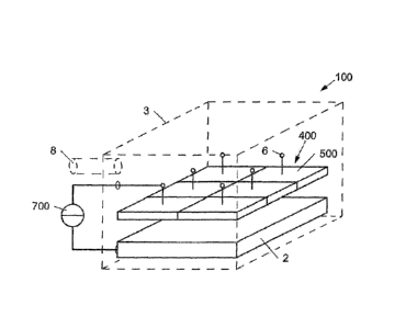
Fig. 1 shows an apparatus 100 for the plasma coating of a substrate 2
comprising a vacuum
chamber 3 and a therein arranged electrode 400, which is in the operational
state oriented to
be essentially parallel to said substrate 2 and opposite its face to be
coated. With respect to the
following considerations it is assumed that the substrate is a press platen 2.
It is naturally also
possible to transpose the following teaching to other substrates.
The electrode 400 is segmented and each segment 500 has a connection 6
dedicated for an
electrical energy source 700, which is configured to be a power source in the
present example.
It is naturally also possible to realize the energy source as a voltage
supply, for instance. Fi-
nally, Fig. 1 also shows a connection 8 for introducing a process gas (e.g. CI-
14) into the vac-
uum chamber 3 where there is a pressure of approximately 1 mbar, for instance.
It is preferred if the area of an electrode segment 500 is smaller than or
equal to 1 m2, and the
current intensity of a power source 700 is less than or equal to 150 A. These
values are a
CA 02881069 2015-02-05
"' 11 -
good compromise wherein the good results of a coating of the press platen 2
are achieved
while the electrode 400 is not segmented too heavily and the risk of a
destructive electric
flashover between electrode 400 and press platen 2 is not too high.
It is generally possible for the energy source 700 to supply direct current or
alternating cur-
rent. A particular good coating of the press platen 2 is achieved by impulse-
type current. In
this case, the current amplitude of the impulses are preferably smaller than
150 A. The polar-
ity of the pulses can also be reversed from time to time if away electrical
loads at the applied
layer are to be led away, e.g. if electrically insulating layers are being
applied. It is for in-
stance possible that one of ten pulses has a different polarity.
Fig. 2 shows an example of an electrode 401, the segments 501 of which are
fully insulated
from one another. The individual segments 501 are accordingly only provided in
the form of
conductive plates spaced apart from one another. These can for instance be
applied to a non-
conductive substrate so that the handling of the electrode 401 is easier. In
order for the pro-
cess gas to reach the press platen 2 more easily, in particular through
recesses in the afore-
mentioned substrate in the region between the segments 501, the electrode 401
may have
holes. These holes can be provided in the form of elongated holes, for example
(see also Fig.
3).
Fig. 3 shows another example of an electrode 402, the segments 502 of which
are connected
with one another via small webs 9 and consequently without (high) Ohm
resistances. It is
thus generally possible that the electrode 402 is provided in one piece, for
instance, by mill-
ing, cutting, nibbling or laser-cutting the corresponding recesses 10 into a
sheet.
Fig. 4 shows a further example of an electrode 403 where the electrode
segments 503 are con-
figured to be grid-like. It is thereby even easier for the process gas to
reach the press platen 2.
Fig. 5 illustrates another example of an electrode 404 which is formed from
circular electrode
segments 504 and check-shaped electrode segments 505. This is a purely
illustrative example
and only showing that it is not absolutely required for an electrode 400 to be
provided in the
form of rectangular electrode segments 500. Apart from the shapes illustrated
in Fig. 5, a plu-
rality of other non-rectangular shapes may be used.
= CA 02881069 2015-02-05
- 12 -
Fig. 6 shows an example of an electrode 405 which is in its edge region bent
in the direction
of the press platen 2 to be coated. In the specific case, the electrode
segments 506 are ar-
ranged to be parallel with the press platen 2, whereas the electrode segments
507 are tilted in
the direction of the press platen 2 or - as in the present example - bent in
the direction of the
press platen 2. In this way, a drop of the electrical field strength in the
plasma, such as that re-
sulting from a plate-shaped electrode which is also in the edge region of the
press platen 2 ori-
ented to be parallel with the latter, can be compensated.
Alternatively or additionally to the embodiment as shown in Fig. 6 it is for
instance also con-
ceivable that segments 500 located in the edge region of the electrode 400
(see also Fig. 11)
are arranged to be closer to the press platen 2 than inner segments. In
particular all segments
500 can be arranged to be parallel with the press platen 2.
A method for manufacturing a press platen 2 now comprises the following steps:
a) arranging a press platen 2 to be coated in a vacuum chamber 3 opposite a
seg-
mented electrode 400 arranged in the vacuum chamber 3 and aligned to be
essentially parallel
with the electrode,
b) activating at least one energy source 700 that is assigned to an
electrode segment
500 and
c) introducing a gas which causes a plasma-enhanced chemical vapor
deposition on
the press platen blank 2.
For the sake of completeness it should be noted at this stage that step c) may
naturally be car-
ried out prior to step b).
It is only for illustrative reasons, that Fig. 1 shows only one single energy
source 700, which
is connected with an electrode segment 500. This can principally be connected
with the dif-
ferent electrode segments 500 one after the other. It is alternatively also
conceivable that an
apparatus for the plasma coating of a press platen 2 comprises several energy
sources 700
which can be open-loop/closed-loop controlled independently of one another,
which energy
sources 700 can be connected with the electrode segments 500 via the
connections 6.
= CA 02881069 2015-02-05
- 13 -
To this end, Fig. 7 shows an illustrative example where a control unit 1101 of
an apparatus
101 (here illustrated without vacuum chamber 3) is configured so as to switch,
with the aid of
the switches 1201 and 1202, one energy source 701, 702 to one electrode
segment 508 of a
group 1301, 1302 of electrode segments 508, and to switch the connections of
the other elec-
trode segments 508 of this group to an open-state insulated from the firstly
mentioned elec-
trode segment 508 (the press platen 2 of this example and the further examples
is connected to
the ground). In specific terms, the electrode segments 508 in the embodiment
illustrated as an
example in Fig. 7 are divided into two groups 1301 and 1302, the first group
1301 comprising
three electrode segments 508 of identical size and the second group 1302
comprising five
electrode segments 508 differing in size. The division is of purely
illustrative character and is
to demonstrate that the electrode segments 508 of an electrode 406 are not
required to be of
identical size. Fig. 7 furthermore shows that the electrode segments 508 are
not required to
have quadratic shape, but can also have a general rectangular shape. The
electrode segments
508 can in particular be embodied to have the shape of bands, rods and/or
strips. A first en-
ergy source 701 is now switched to one electrode segment 508 of the group
1301, a second
energy source 702 is switched to one electrode segment 508 of group 1302. The
other elec-
trode segments 508 are switched to an open-state.
Once a certain period of time has passed, the assignments between the energy
sources 701,
702 and the electrode segments 508 are changed. This means that the energy
source 701 is
connected with another electrode segment 508 of group 1301 and the previously
connected
electrode segment 508 is switched to an open-state. By analogy, the energy
source 702 is con-
nected with another electrode segment 508 of group 1302 and the previously
connected elec-
trode segment 508 is switched to an open-state. It is thereby possible to
connect all electrode
segments 508 of the groups 1301 and 1302 with the energy sources 701 and 702
one after the
other. This allows all electrode segments 508 to be supplied independently of
one another
with energy by means of only a low number of energy sources 701, 702.
The electrode segments 508 assigned to the activated energy source 701, 702
can be a result
of a random selection or a result of a predetermined scheme. The electrode
segments 508 are
not required to be connected with the energy source 701, 702 in the same order
in each cycle.
It is also possible that one electrode segment 508 is connected with the
energy source 701,
702 several times in the course of one cycle.
CA 2881069 2017-03-06
- 14 -
A particularly advantageous method is provided if electrode segments arranged
so as to
correspond to the white squares of a chessboard and electrode segments
arranged so as to
correspond to the black squares of a chessboard are supplied with electrical
energy in
alternation. To this end, Fig. 8 shows an illustrative example of an electrode
407 where the
electrode segments 509 are arranged in a 6x9 matrix, in order to emphasize
that it is not
necessarily required for the electrode segment 509 to be arranged in a 8x8
matrix, as it is the
case with a chessboard. In accordance with this variant, the "white" segments
509 are activated
in a first period of time, in a second period of time, the "black" segments
509 (illustrated with
hatched lines) are activated.
When an energy source 701, 702 is being assigned to an electrode segment 508,
it is principally
possible to predetermine a current intensity and/or a potential of the same.
The remaining
electrode segments 508 which are not assigned to an energy source 701, 702 are
switched to an
open-state, wherein they are insulated from the energy source 701, 702 or from
the thereto
connected electrode segment 508. The current for these electrode segments 508
is consequently
naught, or it is possible that there is only a low compensating current
flowing between the
segments 508. Accordingly, the potential can virtually have any value
("floating potential").
Fig. 9 shows an electrode 408 where there is one electrode segment 510
connected with one
energy source 701, 702 each, which can be open-loop/closed-loop controlled
independently of
the remaining energy sources 701..706. In other words, the energy source 701
can be open-
loop/closed-loop controlled independently of the energy sources 702..706, etc.
Accordingly,
one energy source 701..706 is activated per each electrode segment 501 and
open-loop/closed-
loop controlled independently of the remaining energy sources 701..706. It is
thereby possible
to supply nearly all electrode segments 510 with energy independently of one
another. It is for
instance possible that for each electrode segment 501 a particular current
intensity and/or a
particular potential is provided and - in case the energy source 701..706 is
closed-loop
controlled - also adhered to with varying procedural conditions.
In another example illustrated in Fig. 10, the voltage between an electrode
segment 511 and the
press platen 2 to be coated is ineasured with the aid of a voltmeter 14, and
the energy supply
700 is limited by means of a control unit 1102 and/or the supply of current to
the electrode
CA 02881069 2015-02-05
- 15 -
segment 511 is switched off using a switch 1200 operated by the control unit
1102, if a drop
of said voltage is detected. The voltmeter 14 can for instance be provided in
the form of an
analogue-digital-converter which is connected to a microcontroller where e.g.
also the control
unit 1102 can be integrated in. In this way, an electrical flashover between
the electrode seg-
ment 511 and the press platen can be detected and its destructive effect can
be limited. It is
moreover also possible to actively terminate the flashover by means of the
above-mentioned
measures. Of course, also a common control unit for the functionality of the
control unit 1101
illustrated in Fig. 7 and the control unit 1102 illustrated in Fig. 10 can be
provided.
Fig. 11. illustrates a further variant of the method for the plasma coating of
a press platen 2,
where segments 512 (indicated by hatched lines) located at the edge of an
electrode 409 are
set at a higher potential and/or set/regulated to a higher current intensity
than inner segments
512 (in white). It is thereby possible to compensate a drop of the electric
field strength in the
plasma - as it results from a board-type electrode 409 arranged to be parallel
with the press
platen 2 - (see also Fig. 6) and/or to provide the press platen with a thicker
layer at its edge.
These regions of the press platens 2 are usually subjected to the highest
stress during the man-
ufacture of plate-shaped materials.
Fig. 12 finally shows a schematic example where the electrode segments 510 are
connected
with an energy supply 700 via resistances 15. By providing different
resistances 15 this vari-
ant may advantageously allow the electrode segments 510 to be differently
supplied with en-
ergy by means of only one energy source 700. It is naturally also possible to
provide identical
resistances 15. Additionally, the probability for the occurrence of an
electric flashover in the
plasma is significantly moderated, or the effects of the latter are noticeably
reduced as the re-
sistances 15 impede a concentration of electrical energy in one individual
electrode segment
510. The arrangement 103 illustrated in Fig. 12 can naturally also be used in
combination
with the already illustrated arrangements. The arrangement of several energy
sources instead
of one single energy source 700 is possible, for instance. It is moreover also
conceivable that
further, not shown resistances are arranged between the electrode segments
510, for instance
as the electrode 408 is embodied according to the Figs. 3 and 4. It is finally
also conceivable
that the resistances 15 are provided in the form of narrow terminals 6, in
particular if compa-
rably high currents are to be led to the electrode segment 510.
CA 02881069 2015-02-05
- 16 -
The embodiments illustrated as examples represent possible variants of the
apparatus 100..103
for the plasma coating of a substrate, and it should be pointed out at this
stage that the inven-
tion is not specifically limited to the variants specifically illustrated, and
instead the individual
variants may be used in different combinations with one another and these
possible variations
lie within the reach of the person skilled in this technical field given the
disclosed technical
teaching. Accordingly, all conceivable design variants which can be obtained
by combining
individual details of the design variants described and illustrated are
possible and fall within
the scope of the invention.
-- It is in particular stated that said apparatus 100..103 may in reality also
comprise more com-
ponents than those illustrated. It is in particular pointed out the disclosed
teaching is indeed
particularly advantageous in connection with pressing platens, it may however
be unrestrict-
edly transposed to other substrates, such as to those for deep drawing,
extrusion and pressing
tools in general.
The described substrates 2 or the press platens are specifically suitable for
the manufacturing
of single-layer or multi-layer board-type materials. This shall in particular
mean thermoplastic
and duroplastic such as epoxy resins, polyester resins and phenolic resins at
least the surfaces
facing the press platen 2 of which are charged with particles having a Vickers
hardness be-
-- tween 1000 and 1800 or also with corundum particles (A1203) in order to
provide a better fric-
tion wear resistance. It is likewise possible to manufacture wood fiber
materials such as chip-
boards, medium-density fiberboards (MDF) and high-density fiberboards. For
manufacturing
a laminate it is in particular possible to coat these wood materials with
layers of plastic of the
aforementioned type or with paper. Furthermore, it is also easily possible to
provide glass fi-
-- ber reinforced plastic or carbon fiber reinforced plastic with a surface
structure. It is finally
also possible to produce artificial stone or "engineered stone" (composite
material of stone
and resin). In particular when using hard rock, such as granite, a long useful
lifetime of the
disclosed substrates 2 or press platens turns out to be advantageous.
-- For the sake of good order, finally, it should be pointed out that, in
order to provide a clearer
understanding of the structure of the apparatus 100..103 for the plasma
coating of a substrate
2, it and its constituent parts are illustrated to a certain extent out of
scale and/or on an en-
larged scale and/or on a reduced scale.
CA 02881069 2015-02-05
= , ,
=
- 17 -
The objective underlying the independent inventive solutions may be found in
the description.
CA 02881069 2015-02-05
=
- 18 -
List of reference numerals
100..103 Apparatus for the plasma
coating
2 Substrate (pressing platen)
3 Vacuum chamber
400..409 Electrode
500..512 Electrode segment
6 Electrode connection
700..702 Energy source
8 Gas connection
9 Web
Recess
1101, 1102 Control unit
1201, 1202 Switch
1301, 1302 Group of electrode seg-
ments
14 Voltmeter
(Ohm) resistance