Note: Descriptions are shown in the official language in which they were submitted.
CA 02881328 2015-04-13
RED-003-CA-DIV3
EMBEDDED POWER CONTROL IN A HIGH-SPEED CABLE
The present invention is a divisional of Canadian Patent Application No.
2,664,597, filed
July 19, 2007.
FIELD OF THE INVENTION
The present invention relates to high speed cables that carry serially encoded
differential
signals between electronic equipments, and in particular, multi-conductor
cables interconnecting
audio-visual equipment.
BACKGROUND OF THE INVENTION
The distribution of television signals has increasingly become based on
digital methods and
digitally encoded forms of video and audio signals. At the same time, higher
resolution (high
definition TV) has become available in the market place, commensurate with
larger and higher
definition displays. To meet the requirement of interconnecting such high
definition displays with
digital signal sources such as Digital Versatile Disc (DVD) players and
receivers/decoders for digital
satellite and digital cable distribution of video material, a digital
interface standard has evolved,
known as the High-Definition Multimedia Interface (HDMI). A detailed
specification for HDMI can
be obtained from the "hdmi.org" website. The HDMI specification currently
available and used in
this application is HDMI specification version 1.3 dated June 22, 2006. This
HDM1 standard can be
employed for connecting digital video sources to digital video sinks over a
cable that carries a
number of digital signals and a clock signal.
The inherent characteristics and manufacturing imperfections of high-speed
differential
signaling cables such as may be used to carry HDMI signals have an adverse
effect on the
high-speed signals carried by the cable.
For example, any cable has a limited bandwidth and therefore acts as a low
pass filter. The
bandwidth of the cable is related to its length, the longer the cable the
greater the filtering effect and
the lower its bandwidth. As a result, high-frequency signals passing through
the cable are
attenuated, and their edges become less sharp. This leads to an increased risk
of misinterpreting the
received data at the receiver end of the cable, especially for long cables and
high-speed data.
1
CA 02881328 2015-02-05
RED-003-CA-DIV3
Figures 1A-1C illustrate the effect of the limited bandwidth of a cable on the
transmitted
signals. Figure 1A illustrates a high-speed signal to be transmitted through a
high-speed cable,
Figure 1B shows a distorted bandwidth-limited signal received at the receiver
end of the cable
(before equalization), and Figure 1C shows the received signal at the receiver
end after equalization.
As seen from Figure 1B, the signal edges are slowed and short pulses are
narrowed, not reaching the
full transmitted amplitude.
Differential signaling cables are commonly used to carry high-speed digital
signals in
differential form, that is pulses of opposing polarities are transmitted on
the two strands of the cable.
The differential signal carried over such cables may be warped, that is the
two signal components
(positive and negative polarities V+ and V-) are skewed in time with respect
to each other
(differential skew), further distorting the received signal.
The impact of differential skew is depicted in timing diagrams in Figures 2A
and 2B.
Figure 2A shows an example timing diagram of the two single ended signal
components
(V+, V-) of the differential data on an HDMI channel, as it may be transmitted
by an HDMI source
into a cable. A timing diagram of the corresponding differential signal (Vdiff-
xmit) in Fig. 2A
illustrates the corresponding differential signal that is clean and easily
interpreted.
Figure 2B shows an example timing diagram of the two single ended signal
components
(V+ and V-del) of the differential data on an HDMI channel, as it might be
received at the end of a
cable. For the sake of clarity, only the effect of the differential skew is
shown in Fig. 2B. The
signals V+ and V- are skewed in time with respect to each other. The negative
signal component V-
is delayed with respect to the signal component V+ by a differential skew
delay of Td. A timing
diagram of the corresponding distorted differential signal (Vdiff-rcv) in Fig.
2B illustrates that, as a
consequence of the differential skew, the differential signal Vdiff-rcv is
significantly distorted with
clearly visible plateaus in the signal where the differential signal is zero
(0). These plateau regions
can only be interpreted as noise by the receiver, the result of which is to
reduce the width of the
window of valid data. This reduction is seen as a closure of the receive data
eye and directly
compromises the channel quality. The amount of differential skew delay (Td)
depends on the
characteristics of each individual cable, and is basically constant.
Earlier approaches to improving cable quality so far have been limited to
embedded passive
equalizer circuits within the cable, which boost high frequencies of the
signals attenuated in the
cable. Such equalizers are fixed to compensate for a fixed cable length.
2
CA 02881328 2015-02-05
RED-003-CA-DIV3
While the equalization required for a given cable depends largely on the
length of the cable,
other characteristics of high-speed signaling cables such as the differential
skew, being more
random, may vary substantially between the cables.
Accordingly, there is a need in the industry for the development of an
improved high-speed
signaling cable, which would provide improved signal characteristics.
Earlier High-Definition Multimedia Interface (HDMI) signal boosters that can
be used to
boost HDMI signals use external power inputs, see e.g. Long ReachTM product of
Gennum
corporation, which can be found at www.gennum.com/ip/pdffiles/gs8101.pdf. As a
result, they
cannot be embedded in a standard HDMI cable. A more recent development is a
stand-alone "super
booster" that can be inserted inline with a cable, and is also available
integrated in an HDMI cable,
see references: Gefen Inc., http://www.gefen.com/kvm/product.jsp?prod id=2939,
including an
advertisement of a standalone HDMI "super booster; A manual for the standalone
HDMI "super
booster, which can be found at http://www.gefen.com/pdf/EXT-HDMI-141SB.pdf;
and an
advertisement for a cable with an integrated HDMI "super booster"
http://www.gefen.com/kvm/cables/hdmicables.jsp#hdmisb
The possibility of embedding an active device within the cable is associated
with a problem.
Firstly, no power input may be available for such a device except through the
cable, i.e. there is no
provision for external power supplies. Secondly, in the case of the HDMI
cable, there is not enough
power available to power a simple signal regenerator, primarily because of the
specification
requirement to provide a termination voltage for the inputs. As a result, the
embedded active device
apparently cannot be powered as required.
In more detail, the main power requirement for an HDMI signal booster is the
requirement to
provide a termination voltage (3.3V) with the capability to source 12mA for
each of three HDMI
inputs. The power that is available from the cable comes from a 5V line, from
which a maximum
current of 5mA can be drawn (as per HDMI specification V1.3) when the sink
device is active, i.e.
the total available power is limited to 50mW. The combined power requirement
of the input
terminations on the other hand is approximately 12mA*3.3V*3 = 120mW.
Unfortunately, these
requirements cannot be met in a standard HDMI cable in a simple way.
Accordingly, there is a need in the industry for the development of an
improved signal
booster with an improved power control circuit for embedded cable applications
based on one or
more active devices, which would avoid or mitigate the above noted problem.
3
CA 02881328 2015-02-05
RED-003-CA-DIV3
SUMMARY OF THE INVENTION
There is an object of the invention to provide an improved programmable cable
with
embedded power control and boost device as well as methods and systems for
calibrating the cable.
According to one aspect of the invention there is provided a cable for
connecting a
transmitting data source device to a receiving data sink device and carrying
differential data signals
including: a boost device for boosting at least one of the differential data
signals, the boost device
comprising: an electronic circuit for obiaining at least some of the
electrical power required to
operate the boost device from the at least one of the differential data
signals.
The differential data signals are differential High Definition Multi-Media
Interface (HDMI)
signals and include a plurality of Transition Minimized Differential Signaling
(TMDS) encoded data
channels and a clock channel.
The boost device includes: a differential input circuit for receiving one of
the differential
data signals from the data source device; and a differential output circuit
for transmitting a boosted
one of the differential data signals to the data sink device, wherein said at
least some of the electrical
power is obtained from the data source and sink devices.
The differential output circuit and the differential input circuit are
connected in series so as
to conduct a current from the data sink device to the data source device.
The differential output circuit and the differential input circuit are joined
at an intermediate
voltage node such that load current from the data sink device flows through
the differential output
circuit to the intermediate voltage node, and the intermediate voltage node is
connected as the
supply voltage for the differential input circuit.
The cable further includes a voltage boost circuit between the intermediate
voltage node and
a second intermediate voltage node supplying voltage for the differential
input circuit.
The voltage boost circuit includes a switched capacitor and a 2-phase clock,
the capacitors
used for periodically transferring energy from the intermediate voltage node
to the second
intermediate voltage node.
The boost device further includes a processing block having a transfer
function for
processing the differential signal received by the differential input circuit
and conveying the
processed signal to the differential output circuit.
The cable further includes a power converter for converting the power for
operating the
4
CA 02881328 2015-02-05
RED-003-CA-DIV3
processing block from an available higher voltage, the power converter
comprising switched
capacitors and a 2-phase clock, the switched capacitors used for transferring
energy from the
available higher voltage to the processing block.
According to another aspect of the invention, there is provided a method for
providing
power to a boost device in a cable connected between a transmitting data
source device and a
receiving data sink device, comprising the steps of: receiving differential
data signals from the data
source device in a differential input circuit of the boost device; boosting at
least one of the received
differential data signals into a boosted differential data signal;
transmitting the boosted differential
data signal to the receiving data sink device with a differential output
circuit of the boost device; and
obtaining power to operate at least some of the circuitry of the boost device
from the data source
and sink devices through their connections with the differential input and
output circuits
respectively.
The method further comprises the step of connecting the differential output
circuit and the
differential input circuit in series so as to conduct a current from the data
sink device to the data
source device.
The method as described above further comprises the steps of: joining the
differential output
circuit and the differential input circuit at an intermediate voltage node
such that load current from
the data sink device flows through the differential output circuit to the
intermediate voltage node;
and connecting the intermediate voltage node as the supply voltage for the
differential input circuit.
According to yet another aspect of the invention there is provided a boost
device for
connecting a transmitting data source device to a receiving data sink device,
the transmitting data
source device sending differential data signals into the boost device, the
boost device for boosting at
least one of the differential data signals, the boost device comprising an
electronic circuit which
obtains at least some of the electrical power required to operate the boost
device from the at least
one of the differential data signals.
In the boost device as described above, the differential data signals are
differential High
Definition Multi-Media Interface (HDMI) signals and include a plurality of
Transition Minimized
Differential Signaling (TMDS) encoded data channels and a clock channel.
The boost device further comprises: a differential input circuit for receiving
one of the
differential data signals from the data source device; and a differential
output circuit for transmitting
a boosted one of the differential data signals to the data sink device;
wherein said at least some of
5
CA 02881328 2015-02-05
RED-003-CA-DIV3
the electrical power to operate the boost device is obtained from the data
source and sink devices.
In the boost device described above, the differential output circuit and the
differential input
circuit are connected in series so as to conduct a current from the data sink
device to the data source
device.
The differential output circuit and the differential input circuit are joined
at an intermediate
voltage node such that load current from the data sink device flows through
the differential output
circuit to the intermediate voltage node, and the intermediate voltage node is
connected as the
supply voltage for the differential input circuit.
The boost device described above further includes a voltage boost circuit
between the
intermediate voltage node and a second intermediate voltage node supplying
voltage for the
differential input circuit.
The voltage boost circuit includes a switched capacitor and a 2-phase clock,
the capacitor
used for periodically transferring energy from the intermediate voltage node
to the second
intermediate voltage node.
The boost device further comprises a processing block having a transfer
function for
processing the differential signal received by the differential input circuit
and conveying the
processed signal to the differential output circuit.
The boost device further comprises a power converter for converting the power
for operating
the processing block from an available higher voltage, the power converter
comprising switched
capacitors and a 2-phase clock, the switched capacitors used for transferring
energy from the
available higher voltage to the processing block.
According to one more aspects of the invention there is provided a cable for
connecting a
transmitting data source device to a receiving data sink device carrying
differential signals
including: a boost device for boosting at least one of the differential
signals, the boost device
comprising: an input circuit for receiving a raw differential signal from the
data source device and
outputting a recovered signal; a deskew circuit with first adjustable
parameters for processing the
recovered signal into a deskewed signal; an equalizer circuit with second
adjustable parameters for
processing the deskewed signal into an equalized signal; and an output circuit
for amplifying the
equalized signal into a boosted signal and sending the boosted signal to the
data sink device.
In the cable described above, the boost device further includes a parameter
memory for
6
CA 02881328 2015-02-05
RED-003-CA-DIV3
retaining the first and second adjustable parameters after they have been
adjusted.
The cable further includes a control bus, and the parameter memory is
accessible from said
control bus.
The equalizer circuit comprises a circuit for adjusting a frequency response
of the deskewed
signal by changing the second adjustable parameters to produce the equalized
signal. Preferably, the
equalizer circuit has at least two settings of the second adjustable
parameters for adjusting the
frequency response.
In the cable of the embodiments of the invention, the deskew circuit is an
analog differential
deskew circuit for adjusting an existing time skew of two polarities of the
differential signal by
changing the first adjustable parameters.
The analog differential deskew circuit comprises: a number of delay units
arranged
sequentially; an analog selector, selecting a composite delay resulting from
the delay units that are
selected by the analog selector; and analog switches inserting the composite
delay into the polarities
of the differential signal.
The analog switches are inserting the composite delay into one or the other
polarity of the
differential signal. Preferably, each of the analog delay units has a gain,
which is substantially equal
to 1.0, and each of the analog delay units comprises one or more amplifiers.
In more detail, each
analog delay unit comprises: first and second amplifiers having a common
input, which is the input
of the analog delay unit, and their outputs being summed to generate the
output of the analog delay
unit; the first amplifier having a gain of (1.0 - A), and a delay equal to a
predetermined delay value;
and the second amplifier having a gain of A, and substantially the same delay
as the first amplifier.
Conveniently, the first amplifier is a follower stage, and e second amplifier
has a shunt capacitor for
setting the gain of A.
According to one more aspect of the invention there is provided a boost device
for
connecting a transmitting data source device to a receiving data sink device,
the transmitting data
source device sending differential data signals into the boost device, the
boost device for boosting at
least one of the differential data signals, the boost device comprising: an
input circuit for receiving a
raw differential signal from the data source device and outputting a recovered
signal; a deskew
circuit with first adjustable parameters for processing the recovered signal
into a deskewed signal;
an equalizer circuit with second adjustable parameters for processing the
deskewed signal into an
equalized signal; and an output circuit for amplifying the equalized signal
into a boosted signal and
7
CA 02881328 2015-02-05
RED-003-CA-DIV3
sending the boosted signal to the data sink device.
The boost device further includes a parameter memory for retaining the first
and second
adjustable parameters. The boost device also includes a control input for
accessing the parameter
memory.
The equalizer circuit comprises a circuit for adjusting a frequency response
of the deskewed
signal by changing the second adjustable parameters to produce the equalized
signal. The equalizer
circuit has at least two settings of the second adjustable parameters for
adjusting the frequency
response.
The deskew circuit is an analog differential deskew circuit for adjusting an
existing time
skew of two polarities of the differential signal by changing the first
adjustable parameters.
Preferably, the analog differential deskew circuit comprises: a number of
delay units
arranged sequentially; an analog selector, selecting a composite delay
resulting from the delay units
that are selected by the analog selector; and analog switches inserting the
composite delay into the
polarities of the differential signal. Advantageously, the analog switches are
inserting the composite
delay into one or the other polarity of the differential signal.
Preferably, each of the analog delay units has a gain, which is substantially
equal to 1.0 and
comprises one or more amplifiers. In the embodiments of the invention, each
analog delay unit
comprises: first and second amplifiers having a common input, which is the
input of the analog
delay unit, and their outputs being summed to generate the output of the
analog delay unit; the first
amplifier having a gain of (1.0¨ A), and a delay equal to a predetermined
delay value; and the
second amplifier having a gain of A, and substantially the same delay as the
first amplifier.
Conveniently, the first amplifier is a follower stage, and the second
amplifier has a shunt
capacitor for setting the gain of A.
According to yet one more aspect of the invention, there is provided a method
for sending
differential signals from a transmitting data source device to a receiving
data sink device through a
cable that includes a boost device for boosting at least one of the
differential signals, comprising the
steps of: receiving a raw differential signal from the data source device in
an input circuit of the
boost device and outputting a recovered signal; processing the recovered
signal in a deskew circuit
with first adjustable parameters into a deskewed signal; processing the
deskewed signal in an
equalizer circuit with second adjustable parameters into an equalized signal;
amplifying the
equalized signal in an output circuit into a boosted signal; and sending the
boosted signal to the data
8
CA 02881328 2015-02-05
RED-003-CA-DIV3
sink device.
The method further includes the steps of adjusting the first and second
adjustable
parameters; storing the first and second adjustable parameters in parameter
memory; and accessing
the parameter memory from a control input. Conveniently, the step of
processing the recovered
signal includes the step of adjusting an existing time skew of two polarities
of the differential signal
by changing the first adjustable parameters; and adjusting a frequency
response of the deskewed
signal by changing the second adjustable parameters.
In more detail, the step of changing the first adjustable parameters comprises
the steps of
arranging the number of delay units sequentially; selecting a composite delay
resulting from number
of delay units; and inserting the composite delay into the polarities of the
differential signal.
Beneficially, the step of inserting the composite delay includes inserting the
composite delay into
one or the other polarity of the differential signal. Conveniently, the step
of arranging a number of
delay units includes a step of selecting analog delay units each having a gain
that is substantially
equal to 1Ø
According to one more aspect of the invention, there is provided a cable for
connecting a
transmitting data source device to a receiving data sink device carrying
differential signals
including: a printed circuit board (PCB) and a boost device, the PCB including
tracks for providing
delays in coupling a raw differential signal from the data source device to
two or more inputs of the
boost device; the boost device for boosting at least one of the differential
signals, the boost device
comprising: an input circuit for terminating the delayed raw differential
signal; an input selector
circuit with first adjustable parameters for selecting a delayed raw
differential signal and outputting
a recovered signal that is deskewed; an equalizer circuit with second
adjustable parameters for
processing the recovered signal into an equalized signal; and an output
circuit for amplifying the
equalized signal into a boosted signal and sending the boosted signal to the
data sink device.
The boost device further includes a parameter memory for retaining the first
and second
adjustable parameters. The cable also includes a control bus, and the
parameter memory is
accessible from said control bus.
In the boost device, the input selector circuit for selecting the delayed raw
differential signal
for adjusting an existing time skew of two polarities of the differential
signal is controlled by
changing the first adjustable parameters. The equalizer circuit comprises a
circuit for adjusting a
frequency response of the deskewed signal by changing the second adjustable
parameters to produce
9
CA 02881328 2015-02-05
RED-003-CA-DIV3
the equalized signal. Conveniently, the equalizer circuit has at least two
settings of the second
adjustable parameters for adjusting the frequency response.
The PCB comprises a number of tracks providing delays arranged sequentially,
and the input
selector circuit selecting a composite delay resulting from the tracks that
are selected by the input
selector circuit.
According to one more aspect of the invention, there is provided a cable for
connecting a
transmitting data source device to a receiving data sink device carrying
differential signals
including: a printed circuit board (PCB) and a boost device, the PCB including
tracks for providing
delays in coupling a raw differential signal from the data source device to
two or more inputs of the
boost device; the boost device for boosting at least one of the differential
signals, the boost device
comprising: an input circuit for terminating the delayed raw differential
signal; an input selector
circuit with first adjustable parameters for selecting a delayed raw
differential signal and outputting
a recovered signal that is coarsely deskewed; a deskew circuit with second
adjustable parameters for
processing the recovered and coarsely deskewed signal into a finely deskewed
signal; an equalizer
circuit with third adjustable parameters for processing the finely deskewed
signal into an equalized
signal; and an output circuit for amplifying the equalized signal into a
boosted signal and sending
the boosted signal to the data sink device.
Similar to previous embodiments of the invention, the boost device includes a
parameter
memory for retaining the first, second, and third adjustable parameters. The
cable further includes a
control bus, and the parameter memory is accessible from said control bus.
The input selector circuit for selecting the delayed raw differential signal
for coarsely
adjusting an existing time skew of two polarities of the differential signal
is controlled by changing
the first adjustable parameters, and in which the deskew circuit is an analog
differential deskew
circuit for finely adjusting a remaining time skew of two polarities of the
differential signal by
changing the second adjustable parameters.
The equalizer circuit comprises a circuit for adjusting a frequency response
of the deskewed
signal by changing the third adjustable parameters to produce the equalized
signal. The equalizer
circuit has at least two settings of the third adjustable parameters for
adjusting the frequency
response.
The cable as described above, wherein the PCB comprises a number of tracks
providing
delays arranged sequentially, and the input selector circuit selecting a
composite delay resulting
CA 02881328 2015-02-05
RED-003-CA-DIV3
from the tracks that are selected by the input selector circuit, and wherein
further the analog
differential deskew circuit comprises: a number of delay units arranged
sequentially; an analog
selector, selecting a composite delay resulting from the delay units that are
selected by the analog
selector; and analog switches inserting the composite delay into the
polarities of the differential
signal. Beneficially, the analog switches are inserting the composite delay
into one or the other
polarity of the differential signal. Similar to other embodiments described
above, each of the analog
delay units has a gain, which is substantially equal to 1.0 and comprises one
or more amplifiers.
Each analog delay unit comprises: first and second amplifiers having a common
input, which
is the input of the analog delay unit, and their outputs being summed to
generate the output of the
analog delay unit; the first amplifier having a gain of (1.0 - A), and a delay
equal to a predetermined
delay value; and the second amplifier having a gain of A, and substantially
the same delay as the
first amplifier. Conveniently, the first amplifier is a follower stage, and
the second amplifier has a
shunt capacitor for setting the gain of A.
According to yet one more aspect of the invention, there is provided a cable
for connecting a
transmitting data source device to a receiving data sink device carrying
differential signals
including: a boost device for boosting at least one of the differential
signals, the boost device
comprising: an input circuit for receiving a raw differential signal from the
data source device and
outputting a recovered signal; a deskew circuit with adjustable parameters for
processing the
recovered signal into a deskewed signal; and an output circuit for amplifying
the deskewed signal
into a boosted signal and sending the boosted signal to the data sink device.
The boost circuit further includes an equalizer circuit for adjusting the
frequency response of
the deskewed signal.
The boost device also includes a parameter memory for retaining the adjustable
parameters.
The cable further includes a control bus, and the parameter memory is
accessible from said control
bus.
In this embodiment of the invention, the boost device further includes
performance analysis
circuitry for determining the performance of the cable.
The performance analysis circuitry includes: a differential to single-ended
block for
converting the boosted signal to a single-ended signal; a linear phase
compensator to phase-align the
single-ended signal with a common clock signal; an oversampling circuit
providing a digital
representation of the phase-aligned single ended signal (a preprocessed data
signal); and a training
11
CA 02881328 2015-02-05
RED-003-CA-DIV3
function circuit for estimating a quality of the preprocessed data signal, and
adjusting the parameters
of the deskew and equalizer circuitry (by changing the adjustable parameters)
to improve the quality
of the preprocessed data signal.
The training function circuit further comprises: a digital circuit for
estimating the quality of
the preprocessed data signal and generating a Quality Number indicating said
quality; an evaluation
run control circuit for adjusting the parameters of the deskew and equalizer
circuitry to a number of
predetermined settings, and for monitoring a predetermined number of the
oversampled bits for each
setting; a memory for retaining the best setting corresponding to the highest
Quality Number; and a
means for updating the said parameters to the best setting.
The performance analysis circuitry includes means for receiving a start
trigger to the
evaluation run control circuit, and for reporting the best setting over the
control bus.
According to one additional aspect of the invention, there is provided a
method for
determining the performance of a cable comprising a boost device which
receives a differential data
signal, deskews and equalizes the differential data signal according to
adjustable parameters, and
outputs a boosted signal, the boost device further comprising a performance
analysis circuitry,
including steps of: converting the boosted signal to a single-ended signal;
phase-aligning the
single-ended signal with a common clock signal; oversampling the phase-aligned
single ended
signal and generating a preprocessed data signal; estimating a quality of the
preprocessed data
signal; and adjusting the adjustable parameters to improve the quality of
the preprocessed data
signal.
The method as described in claim 29, further comprising an evaluation step
including the
steps of: estimating the quality of the preprocessed data signal and
generating a Quality Number
indicating said quality; adjusting the adjustable parameters to a number of
predetermined settings;
monitoring the preprocessed data signal_ for each setting; retaining the best
setting corresponding to
the highest Quality Number; and updating the adjustable parameters to the best
setting.
The method described above further comprises the steps of: starting the
evaluation method
by receiving a start trigger, and reporting the best setting over a control
bus.
According to one more aspect of the invention, there is provided a cable for
connecting a
transmitting data source device to a receiving data sink device carrying
differential signals
including: a boost device for boosting at least one of the differential
signals, the boost device
comprising: an input circuit for receiving a raw differential signal from the
data source device and
12
CA 02881328 2015-02-05
RED-003-CA-DIV3
outputting a recovered signal; a deskew and equalizer circuits with adjustable
parameters for
processing the recovered signal into a deskewed signal and equalized signal;
an output circuit for
amplifying the deskewed and equalized signal into a boosted signal and sending
the boosted signal
to the data sink device; a parameter memory for storing the adjustable
parameters; and performance
analysis circuitry for determining the performance of the cable.
The cable further comprises a control bus, wherein the parameter memory is
accessible from
the control bus.
In the embodiments of the invention, the performance analysis circuitry
includes: a
differential to single-ended block for converting the boosted signal to a
single-ended signal; a linear
phase compensator to phase-align the single-ended signal with a common clock
signal; an
oversampling circuit providing a digital representation of the phase-aligned
single ended signal to
produce a preprocessed data signal; and a training function circuit for
estimating a quality of the
preprocessed data signal, and adjusting the parameters of the deskew and
equalizer circuits by
changing the adjustable parameters to improve the quality of the preprocessed
data signal.
The training function circuit further comprises: a digital circuit for
estimating the quality of
the preprocessed data signal and generating a Quality Number indicating said
quality; an evaluation
run control circuit for adjusting the parameters of the deskew and equalizer
circuitry to a number of
predetermined settings, and for monitoring a predetermined number of the
oversampled bits for each
setting; a memory for retaining the best setting corresponding to the highest
Quality Number; and a
means for updating the said parameters to the best setting.
The performance analysis circuitry includes means for receiving a start
trigger to the
evaluation run control circuit, and for reporting the best setting over the
control bus.
A system for calibrating the cable described above is also provided,
including: a control
computer attached to the control bus of the cable, and a data pattern
generator attached to the cable
and programmed to send differential signals into the cable; the control
computer is configured to
send a trigger over the control bus to the performance analysis circuitry to
start the evaluation run
control circuit; to receive the best settings from the performance analysis
circuitry; and to load
parameters corresponding to the best settings into the parameter memory over
the control bus.
Alternatively, the system for calibrating the cable described above comprises:
a control
computer attached to the control bus of the cable, and a data pattern
generator attached to the cable
and programmed to send differential signals into the cable; the control
computer is configured to
13
CA 02881328 2015-02-05
RED-003-CA-DIV3
send a trigger over the control bus to the performance analysis circuitry to
start the evaluation run
control circuit; and the performance analysis circuitry is configured to load
parameters
corresponding to the best settings into the parameter memory over the control
bus.
A corresponding method for calibrating a cable for transmitting differential
signals is
provided, the cable including a boost device for deskewing and equalizing the
differential signals,
the boost device having adjustable parameters and a parameter memory, the
method comprising the
steps of: sending a differential data signal into the cable; sending a trigger
to the boost device;
performing a training run in the boost device, wherein the training run
includes the steps of
performing at least two evaluation runs with different settings of the
adjustable parameters and
evaluating the results with each of the at least two settings, retaining the
best settings; and storing
the best settings in the parameter memory.
The step of performing the evaluation run includes the steps of: processing
the differential
data signal into a deskewed signal; processing the deskewed signal into an
equalized signal; and
generating a preprocessed signal, which is a digital representation of the
equalized signal.
The step of evaluating includes lie steps of: determining the run length of
contiguous "1" or
"0" samples in the digital representation of the equalized signal within a
window of at least one bit
period; counting the number of occurrences of selected run lengths during an
observation period of
"N" bits; storing the counted numbers of occurrences in counters according to
the selected run
lengths; and processing the outputs of the counters into a Quality Number
indicating the quality of
the equalized signal.
According to yet one more aspect of the invention, there is provided a system
for calibrating
a cable for transmitting differential signals, the cable including a boost
device for deskewing and
equalizing the differential signals, the boost device having adjustable
parameters and a parameter
memory, the system comprising: means for sending a differential data signal
into the cable; means
for sending a trigger to the boost device; means for performing a training run
in the boost device,
including evaluation means for performing at least two evaluation runs with
different settings of the
adjustable parameters, evaluating the results with each of the at least two
settings and retaining the
best settings; and means for storing the best settings in the parameter
memory.
In the system for calibrating the cable described above, the evaluation means
comprises:
means for processing the differential data signal into a deskewed signal;
means for processing the
deskewed signal into an equalized signal; and means for generating a
preprocessed signal, which is
14
CA 02881328 2015-02-05
RED-003-CA-DIV3
a digital representation of the equalized signal.
The evaluation means comprises: means for determining the run length of
contiguous "1" or
"0" samples in the digital representation of the equalized signal within a
window of at least one bit
period; means for counting the number of occurrences of selected run lengths
during an observation
period of "N" bits; means for storing the counted numbers of occurrences in
counters according to
the selected run lengths; and means for processing the outputs of the counters
into a Quality Number
indicating the quality of the equalized signal.
According to yet one more aspect of the invention, there is provided a system
for calibrating
a cable for transmitting differential signals, including a boost device having
adjustable parameters
and a parameter memory, the system comprising: a network analyzer capable of
sending at least two
signals into a cable input and measuring the response at a cable output; a
computer connected to the
network analyzer and to the parameter memory of the cable, the computer having
a computer
memory; and a computer program code stored in the computer memory for causing
the computer to
perform a calibration of the cable by changing the adjustable parameters and
storing the results in
the parameter memory of the cable.
The computer program code causes the computer to perform the calibration of
the cable by
performing a training run in the boost device, including performing at least
two evaluation runs with
different settings of the adjustable parameters and evaluating performance of
the cable for each of
the settings, and retaining the best settings. The computer program code also
causes the computer to
perform said at least two evaluation runs, each evaluation run including:
processing the differential
data signal into a deskewed signal; processing the deskewed signal into an
equalized signal; and
generating a preprocessed signal, which is a digital representation of the
equalized signal. The
computer program code further causes the computer to evaluate the performance
of the cable for
each of the settings by: determining the run length of contiguous "1" or "0"
samples in the digital
representation of the equalized signal within a window of at least one bit
period; counting the
number of occurrences of selected run lengths during an observation period of
"N" bits; storing the
counted numbers of occurrences in counters according to the selected run
lengths; and processing
the outputs of the counters into a Quality Number indicating the quality of
the equalized signal.
Optionally, the system for calibrating the cable further comprises the cable
to be calibrated.
A method for operating the system for calibrating the cable described above
comprises the
steps of: (a) measuring differential skew of the differential signals at the
cable output; (b) changing
CA 02881328 2015-02-05
RED-003-CA-DIV3
the adjustable parameters and repeating step (a) when the differential skew is
higher than a
predetermined skew threshold; (c) measuring attenuation at each of a
predetermined number of
frequencies; (d) changing the adjustable parameters and repeating step (c)
when the attenuation is
outside a predetermined range at any measured frequency; and (e) storing the
parameters in the
parameter memory.
The method further comprises the steps of: setting the predetermined skew
threshold to the
minimal value observed within a predetermined number of repeats of the step
(a); setting the
predetermined range to a value close to 0 db, and less than a predetermined
limit at each of the
measured frequencies; and setting the predetermined frequency to approximately
a frequency of the
differential signals for which the cable is intended.
Thus, an improved programmable cable with embedded power control and boost
device is
provided along with methods and systems for calibrating the cable.
BRIEF DESCRIPTION OF THE DRAWINGS
Embodiments of the invention will now be described, by way of example, with
reference to
the accompanying drawings in which:
Figures 1A-1C illustrate a high-speed signal to be transmitted through the
high-speed cable, a
distorted bandwidth-limited signal received at the end of the cable (before
equalization), and the
received signal after equalization respectively;
Figures 2A shows timing diagrams of the single ended signal components and the
corresponding
differential signal of the differential data on a differential signaling
channel respectively as they
might be transmitted by a transmitter into a cable;
Figures 2B shows example timing diagrams of the single ended signal components
and the
corresponding differential signal of the differential data as they might be
received from the end of
the cable;
Figure 3 shows a prior art HDMI (High-Definition Multi-Media Interface)
system;
Figure 4 shows an the HDMI system 10 including an improved HDMI cable 20
according to an
embodiment of the present invention;
Figure 5 is a block diagram illustrating the improved HDMI cable 20 of Fig. 4,
including channel
boost circuits 100;
Figure 6 is a more detailed block diagram of the channel boost circuit 100 of
Fig. 5, including a
16
CA 02881328 2015-02-05
RED-003-CA-DIV3
Differential Deskew Circuit 110;
Figure 7 shows a simplified block diagram of the Differential Deskew Circuit
110 of Fig. 6,
including an adjustable delay block 300;
Figure 8 shows the preferred embodiment of the adjustable delay block 300 of
Fig. 7;
Figure 9 shows a simple RC delay circuit that may be used to introduce the
delay (Td) of Fig. 2B;
Figure 10 shows simulation results of the RC circuit of Fig. 9;
Figure 11 shows simulation results of the RC circuit of Fig. 9 with a reduced
time constant;
Figure 12 shows a delay circuit made from a cascade of three RC stages;
Figure 13 shows the waveforms of the trapezoidal input pulse (Vin) and the
waveforms of the
delayed pulses after each stage of the circuit of Fig. 12;
Figure 14 shows the same cascaded delay circuit as in Fig. 12, with two
buffers (amplifiers) added;
Figure 15 shows simulation results of the circuit arrangement of Fig. 14;
Figure 16 shows a simple follower circuit;
Figure 17 shows an AC-coupled follower circuit, derived from the simple
follower circuit of Fig.
16;
Figure 18 illustrates a simplified block diagram of a buffered delay stage 400
which may be an
embodiment of the delay unit 306 of the adjustable delay 300 of Fig. 6;
Figure 19 shows the preferred embodiment of the buffer 404 of the buffered
delay stage 400 of Fig.
18;
Figure 20 shows a simple N-channel follower;
Figure 21 shows an alternative embodiment 404B of the delay stage 306;
Figure 22 shows a simplified transfer function of a cable;
Figure 23 shows a simplified transfer function of a cascade of an equalizer
and a cable;
Figure 24 shows a system diagram of a representative channel 500, including an
optional voltage
booster 514, and a power converter 520;
Figure 25 is a simplified copy 550 of the representative channel 500 of Fig.
24;
Figure 26 shows a block diagram of the optional voltage booster 514 of Fig.
24;
Figure 27 shows a block diagram of the power converter 520 of Fig. 24;
Figure 28 illustrates the improved HDMI cable 20 of Fig. 4, showing external
connections that are
available for use in calibrating the cable;
Figure 29 shows a Real Time Configuration 540, including an expanded boost
device 544 used in
17
CA 02881328 2015-02-05
RED-003-CA-DIV3
the Real Time Cable Calibration method;
Figure 30 shows a simplified block diagram of the expanded boost device 544 of
Fig. 29, including
a Linear Phase Compensator 554, an Oversampling and Reclocking block 556, and
a Training
Function 558;
Figure 31 shows a block diagram of an exemplary implementation of the Linear
Phase
Compensator 554 of Fig. 30, including a Programmable Analogue Delay 568;
Figure 32 illustrates data phase shifting in the Programmable Analogue Delay
568 of Fig. 31, and
oversampling in the Oversampling and Reclocking block 556 of Fig. 30;
Figure 33 shows a simplified block diagram of the preferred embodiment 700 of
the Training
Function 558 of Fig. 30;
Figure 34 shows a high level flow chart of a training run method 800,
depicting the operation of the
Training Function 558 of Fig. 30;
Figure 35 shows a flow chart of an exemplary evaluation run method 900 further
detailing the step
806 of the training run method 800 of Fig. 34;
Figure 36 shows a generic test set up 1000 for Frequency Domain and Time
Domain Calibration
methods;
Figure 37 shows a simplified high level flow chart of an calibration method
1100 that may be used
with the generic test set up 1000 of Fig. 36 in calibrating the Boost Device
30 in the improved
HDMI cable 20 of Fig. 4;
Figure 38 shows an alternative embodiment of the invention, in the form of a
modified improved
HDMI cable 1200; and
Figure 39 shows a modified boost circuit 100A of the modified boost device
1206.
DETAILED DESCRIPTION OF THE EMBODIMENTS OF THE INVENTION
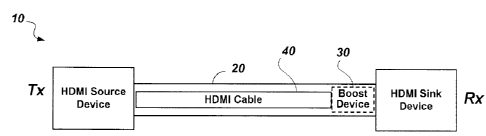
Figure 3 shows a prior art HDMI (High-Definition Multi-Media Interface)
system, including
a HDMI transmitter Tx (HDMI Source Device), a HDMI receiver Rx (HDMI Sink
Device), and an
HDMI cable connecting the Tx and the Rx.
Figure 4 shows an HDMI system 10 including an improved HDMI cable 20 according
to an
embodiment of the present invention.
The HDMI system 10 includes the HDMI transmitter Tx (HDMI Source Device), the
HDMI
receiver Rx (HDMI Sink Device), and the improved HDMI cable 20 of the
embodiment of the
= 18
CA 02881328 2015-02-05
RED-003-CA-DIV3
present invention, connecting the Tx and Rx.
The improved HDMI cable 20 comprises an embedded boost device 30, details of
which are
described in the following, and a basic (passive) HDMI cable 40. The boost
device 30 is located
near the end of the improved HDMI cable 20 closest to the HDMI receiver Rx.
Without limiting the
generality of the application, the improved HDMI cable 20 may be used to
connect a DVD player
(an example of an HDMI Source Device) to a Television Screen (an example of an
HDMI Sink
Device).
Figure 5 is a block diagram illustrating the improved HDMI cable 20 that
extends between
the HDMI transmitter Tx and the HDMI receiver Rx, including the boost device
30 of Fig. 4. Also
shown are HDMI inputs 50 extending from the Tx to the boost device 30 through
the basic HDMI
cable 40, HDMI outputs 52 extending from the boost device 30 to the Rx, and a
group of Other
HDMI Signals 54 extending directly from the Tx to the Rx through the basic
HDMI cable 40. The
basic HDMI cable 40 includes the HDMI inputs 50 and the Other HDMI Signals 54.
The HDMI inputs 50 provide the connections that couple HDMI signals from the
HDMI
transmitter Tx (Fig. 4) over the wires of the basic HDMI cable 40 to inputs of
the boost device 30.
The HDMI inputs 50 include four (4) signal pairs:
- a Transition Minimized Differential Signaling (TMDS) Channel Input 0;
- a TMDS Channel Input 1;
- a TMDS Channel Input 2; and
- a Clock Channel Input.
Similarly, the HDMI outputs 52 include four (4) signal pairs of boosted HDMI
signals:
- a TMDS Channel Output 0;
- a TMDS Channel Output 1;
- a TMDS Channel Output 2; and
- a Clock Channel Output.
The HDMI outputs 52 couple the boosted HDMI signals from the boost device 30
over a
short connection to the HDMI receiver Rx.
A Programming input 56 and a +5V Power signal 58 is coupled from the Other
HDMI
Signals 54 to the boost device 30. Not shown in the figure are physical
features such as device
carrier(s) and connectors which may be part of the improved HDMI cable 20.
The boost device 30 includes a number of channel boost circuits 100, a
parameter memory
19
CA 02881328 2015-02-05
RED-003-CA-DIV3
102. In the preferred embodiment of the invention, the boost device includes
four (4) channel boost
circuits 100 as shown in Fig. 5, each to boost the signal of one of the TMDS
Channel 0, the TMDS
Channel 1, and the TMDS Channel 2.
Each channel boost circuit 100 includes an HDMI Input Circuit 106 and an HDMI
Output
Circuit 108. Each channel boost circuit 100 advantageously further includes a
Differential
(intra-pair) Deskew Circuit 110 for adjusting an existing time skew of the two
polarities of a
differential data signal propagating through the basic HDMI cable 40 and an
Equalizer Circuit 112
to compensate for the limited bandwidth characteristics of the basic HDMI
cable 40. Each channel
boost circuit thus provides a transfer function from the respective HDMI Input
to the corresponding
HDMI Output with characteristics designed to compensate for the degradation of
the corresponding
differential pair in basic cable 40.
The boost device 30 may be powered by the +5V Power signal 58, and by power
derived
from the HDMI Outputs 52 as will be described in detail below. The power for
the operation of the
boost device 30 is entirely derived from signals carried in the improved HDMI
cable 20, and
supplied by the HDMI transmitter Tx and/or the HDMI receiver Rx.
In a cable carrying differential signals, i.e. where each signal is carried
over a pair of wires,
manufacturing tolerances commonly result in slight differences between the
lengths of the wires and
connectors used for each channel. The result will be a different delay through
the cable for each of
the pair. Such differential (intra-pair) skew degrades the received signal
(see Figures 2A and 2B
above). Elimination of intra-pair skew may be accomplished by adding delay to
the signal passing
through the shorter of the pair of wires by the appropriate amount so that it
is aligned with the signal
passing through the longer of the pair. In accordance with the embodiments of
present invention,
intra-pair skew is eliminated with the help of the Differential Deskew Circuit
110, which is digitally
programmable as will be described in the next sections. The parameter memory
102 is used to
retain the deskew settings of the Differential Deskew Circuit 110, once they
are determined in a
programming (calibration) setup method.
Similarly, cables present different bandwidth characteristics, which depend on
the length and
the physical construction of the cable. The limited bandwidth may be
compensated (to some extent)
by the Equalizer Circuit 112 which is also digitally programmable. The
equalizer settings may
similarly be retained in the parameter memory 102. The proper settings for
both the Differential
Deskew Circuit 110 and the Equalizer Circuit 112 may be determined in a
programming
CA 02881328 2015-02-05
RED-003-CA-DIV3
(calibration) setup at the time of production, and loaded into the parameter
memory 102 through the
Programming Input 56. The programming setup method will be described in more
detail further
below (Figs 29 to 37).
Figure 6 shows a more detailed block diagram of a single instance of the
channel boost
circuit 100 of Fig. 5, comprising the HDMI Input circuit 106, the Differential
Deskew circuit 110,
the Equalization circuit 112, and the HDMI Output circuit 108.
The input to the HDMI Input circuit 106 is a raw input signal (pair) 116 (one
of the HDMI
Inputs 50, Fig. 5). The HDMI Input circuit 106 outputs a "recovered signal"
(pair) 118 that is input
to the Differential Deskew circuit 110. The Differential Deskew circuit 110
outputs a "deskewed
signal" (pair) 120 that is input to the Equalization circuit 112. The
Equalization circuit 112 outputs
an "equalized signal" pair 122 that is input to the HDMI Output circuit 108.
And finally, the HDMI
Output circuit 108 outputs a "boosted signal" (pair) 124 that is one of the
HDMI Outputs 52 (Fig. 5).
Also shown in Fig. 6 is the Parameter Memory 102, which is shared among all
channel boost
circuits 100 of the boost device 30. It is connected to a deskew parameter
input 126 of the
Differential Deskew circuit 110, and separately to an equalization parameter
input 128 of the
Equalization circuit 112.
Differential Deskewing Circuit 110
As indicated above, the intra-pair differential skew delay may be compensated
by inserting a
delay element having a delay of Td in the path of V+ (in the case of the
example of Fig. 2B), or in
the path of V- in the opposite case (if the input V+ signal was delayed with
respect to V-), or neither
if there was no skew present.
Figure 7 shows a simplified block diagram of the Differential Deskew Circuit
110 of Fig. 6
in which the differential skew is removed (compensated). The same reference
numerals are used to
indicate the differential inputs and outputs (the recovered signal 118 and the
deskewed signal 120
respectively, each with a positive [NTH and a negative [V-] terminal), and the
control input for the
deskew parameters (126).
As shown in Fig. 7, the Differential Deskew circuit 110 includes an adjustable
delay 300
with a (single-ended) input 302 and an output 304, and six ON/OFF switches Si
to S6. The
adjustable delay 300 includes a number of delay stages 306. The switch Si is
connected between
the positive terminal of the differential input (the recovered signal 118 V+)
and the positive terminal
21
=
CA 02881328 2015-02-05
RED-003-CA-DIV3
of the differential output (the deskewed signal 120 V+). Similarly, the switch
S6 is connected
between the negative terminal of the differential input (the recovered signal
118 V-) and the negative
terminal of the differential output (the deskewed signal 120 V-). The switches
S2 and S4 are
connected between the input 302 of the adjustable delay 300 and the positive
(V+) and negative (V-)
terminals respectively of the recovered signal 118. Similarly, the switches S3
and S5 are connected
between the output 304 of the adjustable delay 300 and the positive (V+) and
negative (V-)
terminals respectively of the deskewed signal 120.
The scheme allows the single adjustable delay 300 to correct for both positive
and negative
differential skew. In effect, the single adjustable delay 300 is sufficient to
compensate positive or
negative differential skew (where either the positive signal or the negative
signal is delayed with
respect to the other), by switching it (the adjustable delay 300) into either
the negative or the
positive signal path respectively. For example, to pass the positive signal V+
through the adjustable
delay 300 (which is made of a cascade of delay units, to be described in
detail below) the switch
states are as follows: S1=OFF, S2=0N, S3=0N, 54=OFF, S5=OFF, and S6=0N. To
pass V- through
the adjustable delay 300 the switch states are as follows: S1=0N, S2=OFF,
S3=OFF, S4=0N,
S5=0N, S6=OFF. To switch the adjustable delay 300 out of both the V- and the
V+ paths, thus
providing no adjustment of the differential delay, the switch states are as
follows: S1=0N, S2=OFF,
S3=OFF, S4=OFF, S5=OFF, S6=0N.
The solution of the deskew problem presents two challenges. The first is to
make a suitable
delay, the second is to tune the delay. Making the delay is a challenge
because the unit should have a
wide enough bandwidth to pass the signals but at the same time the delay block
has to present a
useful delay. The wide bandwidth of a single delay stage naturally results in
little delay, so a cascade
of stages is required to achieve a sufficient delay.
A cascade of digital delay stages, including digital switches and a decoder to
provide binary
addressable selection of the overall delay, are described in United States
Patent 6,268,753.
However, the present invention requires an adjustable delay circuit to delay a
high-speed analog
signal.
Issues to be solved with a cascade of analog delay stages in the proposed
configuration of
Fig. 7 for differential skew compensation, include the need to provide unity
gain, as well as preserve
the high bandwidth required.
Among the prior art, several digital delay compensation schemes are disclosed,
but only few
22
CA 02881328 2015-02-05
RED-003-CA-DIV3
circuits providing adjustable delay for analog signals. For example, the use
of a follower circuit in
parallel with a gain stage to boost the high frequency response of a digital
circuit is taught in United
States Patent 5,739,713. United States Patent 6,525,568 teaches a phase
shifting (delay) stage that
includes an RC (resistor-capacitor) element followed by parallel gain stages
of nominally -1 and +2
gain, their outputs added together to provide overall unity gain with a
particular complex frequency
transfer function. In the United States Patent Application 20050083130 a high
performance
amplifier is proposed which includes a delay element to compensate for signal
propagation delay
that may exist in alternative signal paths.
Figure 8 shows the preferred embodiment of the adjustable delay block 300 of
Fig. 7 as a
cascade of eight analog delay stages ("Delay Units") 306 in combination with
an analog selector
stage 308 as a solution to implement the adjustable delay 300. The eight delay
units 306 are
connected in series (cascaded), the output of each delay unit 306 being input
to the analog selector
stage 308. The first delay unit 306 of the cascade provides the input of the
adjustable delay 300 (IN
302).
The deskew parameters control signal (deskew parameter input 126) includes a 3-
bit binary
signal connected to the analog selector stage 308 for selecting one of its
inputs to be switched
through to the output of the adjustable delay 300 (OUT 304).
An exemplary complete circuit of the single delay unit 306, which may be
cascaded to
provide a unit of delay each, for the adjustable delay 300 is shown in Fig. 18
below.
To help in understanding the circuitry of the single delay unit 306, a step-by-
step description
of the issues to be solved, and possible solutions, is presented first.
Figure 9 shows a simple RC delay circuit that may be used to introduce the
delay (Td) of
Fig. 2B. The circuit of Fig. 9 is a single ended circuit comprising a resistor
Ri, a capacitor Cl, and
input and output terminals (signals Vin and Vout), as well as a ground (0).
The capacitor Cl is
connected between Vout and ground, and the resistor is connected between Vin
and Vout. Making a
circuit with an RC delay as shown in Fig. 9 will succeed in delaying the
signal but it will also filter
the signal.
The impact of the RC circuit of Fig. 9 on a pulse is seen from simulation
results shown in
Figure 10. Fig. 10 shows two simulated wave forms, a trapezoid input pulse
Vin, and an output
pulse (Vout), that results from passing the trapezoid input pulse through the
simple RC delay circuit
of Fig. 9. The trapezoid input pulse (the signal Vin) is delayed and filtered
(distorted) into the output
23
CA 02881328 2015-02-05
RED-003-CA-DIV3
signal Vout. The delay and the filtering action are clearly seen. While the
delay is desirable, the
filtering action causes dispersion and distortion of the pulse.
To reduce the filtering action of the circuit the RC time constant may be
reduced. The
simulated result is shown in Figure 11. The simulation shown in Fig. 11 is
analogous to the
simulation shown in Fig. 10, but with a reduced time constant in the simulated
delay circuit.
Reducing the time constant helps to increase or maintain the bandwidth (note
the slopes of both the
input and output pulses) but as shown in Fig. 11 the signal delay introduced
is lower.
In the simulation of Fig. lithe pulse width is 0.7 second and the RC time
constant in the
circuit is 79ms. The long pulse duration and the long RC time constant were
chosen merely for
convenience in the simulations to study the effects of circuit choices, and
are not representative of
the time scales of the embodiment.
One method of attempting to regain the delay (as shown in Fig. 10 with respect
to the circuit
of Fig. 9 with the original time constant) is to cascade a number of RC
stages. This is shown in
Figure 12. Shown in Fig. 12 is a delay circuit made from a cascade of three RC
stages, comprising
the components R2, C2, R3, C3, R4, and C4, each RC stage having individually
the same time
constant of 79ms. The signals after the first and second stages are labeled V1
and V2 respectively.
The input and output of the circuit as a whole are labeled Vin and Vout.
The result of simulating the circuit of Fig. 12 with a trapezoidal input pulse
is shown in
Figure 13 which shows the waveforms of the trapezoidal input pulse (Vin) and
the waveforms of
the delayed pulses after each stage of the circuit of Fig. 12 (V1, V2, and
Vout). The resulting final
waveform Vout is delayed but it is considerable reduced in amplitude and
dispersed.
In order to remove the loading effect of subsequent stages, each stage may be
buffered as
shown in Figure 14. Shown in Fig. 14 is the same cascaded delay circuit as in
Fig. 12, but two
buffers (amplifiers) are inserted, a buffer "Buf1" between R1 and R2, and a
buffer "Buf2" between
R2 and R3. As a result, the intermediate signals V1 and V2 are not attenuated
by the loads of the
subsequent stages.
The simulation results for the circuit of Fig. 14 are shown in Figure 15. They
show that the
circuit arrangement of Fig. 14 achieves the desired goal of introducing
significant delay while the
distortion in the pulse is kept to a minimum. In this simulation, the 0.7
second trapezoidal input
pulse is delayed by approximately 77ms per stage.
In a mathematical sense, the pulse has been transformed by a cascade of single
pole unity
24
CA 02881328 2015-02-05
RED-003-CA-DIV3
gain stages, the transfer function of each stage being;
H(s) = 1/(1+s/p) where p[Rads] = 1/(RC)
or p[HZ] is 1/(2nRC)
The goal of the circuitry is to delay the pulse by up to about half the pulse
width (bit width).
In the case illustrated in the simulation of Fig. 15, the required delay would
be approximately 0.35
seconds. To achieve this delay with the scheme shown in Fig. 14, this would
require approximately
five stages. In the simulation shown in Fig. 15 the RC time constant is set to
79ms which sets the
pole frequency at 1/(27E79ms) = 2Hz. Thus, with a pulse width of 0.7 seconds
(the input pulse Vin) a
stage with a pole frequency of 2Hz will produce suitable delays with
acceptable filtering on the
pulse. A simple approximation to calculate the position of the pole for a
system with a bit rate of N
bits per second (Nbps) is to set the pole in each stage at 3*N Hz. For
example, with a data rate of
1Gbps, a stage with a pole at approximately 3GHz would be needed.
Having shown how an appropriate delay per stage may be achieved using simple
RC stages,
it remains to be shown how a suitable buffer amplifier (Bufl, Buf2 in Fig. 12)
may be constructed.
To make a unity.gain buffer with unity gain up to 3GHZ is a challenge even on
an advanced CMOS
processes. A starting point would be to use a simple follower circuit as shown
in Figure 16. The
simple follower circuit of Fig. 16 includes an N-channel MOS field-effect
transistor (MOSFET) M1
connected in series with a current source Ii. The drain of the transistor M1
is connected to ground
(0), while the positive terminal of the current source Ii connects to the
supply voltage VDD. The
circuit input (IN) is connected to the gate of the transistor Ml, and its
source provides the circuit
output (OUT).
In this well-known circuit the output OUT follows the input IN with a gain of
approximately
one. The first limitation with this circuit is that the output is typically
level shifted by 0.6 volts or so.
This level shifting is a problem if a number of stages are to be cascaded
because the successive level
shifts will cause the output to rise to the supply voltage and thus the signal
is clipped. To solve this
limitation, AC-coupling is added to the simple follower as shown in Fig. 17.
The circuit shown in
Figure 17 is an AC-coupled follower circuit, derived from the simple follower
circuit of Fig. 16 by
the addition of &capacitor C5 between the circuit input (IN) and the source of
the transistor M1, and
a resistor R5 between the source of the transistor M1 and a bias supply "BIAS"
that provides a
positive bias voltage.
With AC-coupling, the fact that the output of the stage is level shifted up
from the bias level
=
CA 02881328 2015-02-05
RED-003-CA-DIV3
set by "BIAS" in Fig. 17 becomes unimportant when stages are cascaded, because
this level shift is
stored as a constant drop across the input capacitor of the next stage. This
essentially resets the
average input voltage at each stage to be the bias voltage set by the bias
supply (BIAS) shown in
Fig. 17.
A further limitation of this circuit comes from the non-zero output
conductance of the
transistor Ml. The gain of the follower is given by gml/(gml+gds1). Here gml
is the small signal
transconductance and gdsl is the small signal output conductance of Ml.
Clearly, for all values of
gdsl greater than zero the gain of the stage is less than one. When fast
wideband circuits are
required, the length of the MOSFET M1 is reduced to close to minimum. This
causes gdsl to
increase to a point where the gain is now tending to 0.9 or so. A cascade of
these stages would
dramatically reduce the magnitude of the incoming signal.
One possible architecture which corrects for this reduced stage gain is shown
in Figure 18
which illustrates a simplified block diagram of a buffered delay stage 400,
which may be an
embodiment of the delay unit 306 of the adjustable delay 300 (Fig. 6).
The buffered delay stage 400 comprises a unit gain amplifier (buffer) 404. The
buffer 404,
having an input 410 and an output 412.
The buffer 404 includes two amplifiers in parallel, a follower stage 414,
having a gain of
approximately 0.9 and a supplementary stage 416 with a gain of approximately
0.1, both amplifiers
having the same frequency response (expressed mathematically by the pole
1/(1+s/p). Both
amplifiers (414 and 416) share the input 410 of the buffer 404, and their
outputs are summed into
the output 412.
The buffered delay stage 400 provides an inherent delay (implicit in the poles
p of the
transfer functions), and by virtue of the amplifiers, provides the isolation
from the next delay
element in the cascade, as described earlier (Fig. 14). Note that in very high-
speed operation, no
explicit RC delay element is needed if the (by necessity limited) frequency
response of the buffer
404 is designed to provide the required delay.
The buffered delay stage 400 receives the input signal VIN of the buffered
delay stage 400
connected to the input 410 of the buffer 404; and the output 412 of the buffer
404 generates the
output signal VOUT of the buffered delay stage 400.
The preferred embodiment of the buffer 404 including its component amplifiers
(the
follower stage 414 and the supplementary stage 416), is shown in detail in
Figure 19, as a circuit
26
CA 02881328 2015-02-05
RED-003-CA-DIV3
based on an N-well CMOS process.
The follower stage 414 is an AC-coupled circuit, similar to the AC-coupled
follower circuit
of Fig. 17. It comprises a P-channel follower transistor M2, a biasing
resistor R6, a coupling
capacitor C6, and a bias supply "BIAS1".
The supplementary stage 416 includes a N-channel amplifying transistor M3, and
two
P-channel transistors M4 (functioning as a diode) and M5 (functioning as a
current source); a
biasing resistor R7; a coupling capacitor C7; a shunt capacitor C8; and a bias
supply "BIAS2".
The bias voltages of "BIAS1" and "BIAS2" are adapted to the circuit functions
and the
technology as required.
The input 410 of the buffer 404 is connected through the coupling capacitor C6
to the gate of
the transistor M2, and through the coupling capacitor C7 to the gate of the
transistor M3. The
positive terminal of the bias supply "BIAS1" is fed to the gate of the
transistor M2 through the
biasing resistor R6. Similarly, the positive terminal of the bias supply
"BIAS2" is fed to the gate of
the transistor M3 through the biasing resistor R7. The negative terminals of
"BIAS1" and "BIAS2",
the drain of the transistor M2, the source of the transistor M3, and one
terminal of the shunt
capacitor C8 are connected to ground. The other terminal of the shunt
capacitor C8 is connected to
the gate of the transistor M3. The source of the follower transistor M2 is
connected to the drain of
the current source transistor M5 and the output 412 of the buffer 404. The
drains of the transistors
M3 and M4 are connected together, and also to the gate of the transistor M4.
The sources of the
transistors M4 and M5 are connected to the supply voltage VDD.
Functionally, the signal of the input 410 of the buffer 404 is amplified by
the follower stage
414 with a gain of about 0.9, the transistor M5 (in the supplementary stage
416) providing a current
source load to the follower transistor M2. The function of the supplementary
stage 416 is to amplify
a portion of the same input signal (the portion being defined by the ratio of
the coupling capacitor
C7 to the shunt capacitor C8) in the transistor M3 into a varying current that
is mirrored through the
transistors M4 and M5, and so providing a varying current source load to the
follower transistor M2.
Thus, both the follower stage 414 and the supplementary stage 416 contribute
to the signal at the
output 412 of the buffer 404, their individual contributions effectively being
added as indicated in
Fig. 18 above.
The gain of the P-channel follower circuit (414) is essentially unity except
for the output
conductance (gds) of the P-channel device (M2). Because of the requirement for
speed a short
27
CA 02881328 2015-02-05
RED-003-CA-DIV3
P-channel device is required and thus the device has a large output
conductance and the gain falls
toward 0.9. With a cascade of 5 stages the signal would have fallen to 60% of
its original value. To
boost the gain of the simple follower at channel data rates, the parallel
signal path is provided in the
form of the supplementary stage 416.
As described above, the buffer 404 includes a second path (the supplementary
stage 416) for
the input signal (410) to arrive at the output 412. This extra path is through
C7, M3, M4, and M5. In
this path, the high frequency input signal is passed though C7 and a fraction
of the signal is
presented at the gate of M3. This fraction is changed by changing the size of
the shunt capacitor C8.
The current in M3 is set to a nominal value with a bias circuit ("BIAS2").
When the input signal
arrives at the gate of M3 it varies the current in M3. This current variation
is sourced by the diode
connected device (M4) which then mirrors the current change to M5. Finally M5
changes the
current in M2 so the end result is that changing the input signal changes the
current in M2.
Changing the current level in M2 changes the overdrive in the device and thus
changes the output
voltage. In summary a positive change at the input 410 causes a positive
change at the output 412
due to current steering in the parallel path. At the same time there is a
positive change at the output
due to the simple follower action through M2. The overall change in the output
is calculated by
summing the contributions from the Parallel (supplementary stage 416) and Main
(follower stage
414) paths. If the main path is producing a gain of 0.9 the parallel path may
be tuned to provide a
gain of 0.1 by changing the value of C8. Once adjusted to unity, the gain of
the stage remains stable
over Process, Supply Voltage, and Temperature to within about two percent of
its nominal value.
The buffer circuit 404 of Fig. 19 meets the following requirements.
= An overall gain of unity and thus cascading does not amplify or reduce
the signal;
= Capable of very wideband operation (pole at 2GHz to 10GHz) for minimal
distortion; and
= Input and Output levels of a cascade of stages stay within a suitable
range.
Some typical values for the implementation of the buffer 404 are: R6=200k,
R7=200k,
C6=200f, C7=200f, C8 is tuned to adjust the overall gain of the circuit to
unity.
An embodiment of the buffer, equivalent to the buffer circuit 404 shown in
Fig. 19, may be
created by starting with a simple N-channel follower (instead of the P-channel
follower of Fig.16,
that has led to the complete buffer implementation shown here in Fig. 18). The
simple N-channel
follower is shown in Figure 20.
For a CMOS process with a P-Well technology the configuration shown in Fig. 19
would be
28
CA 02881328 2015-02-05
RED-003-CA-DIV3
the preferred implementation in that the bulk of the N-channel Mosfet would be
free to be tied to the
source as shown in Fig. 20. For the more standard CMOS processes with N-Well
technology the
circuit of the buffer of Fig. 19 would cause additional challenges because the
bulk connection on the
N-channel MOSFET is tied to ground. This grounded bulk causes a varying source-
to-bulk potential
in the transistor and further degrades the gain of the stage from 0.9 and this
reduced gain makes it
more difficult to maintain the overall gain of the stage at unity.
An alternative configuration for making the buffer stage for the delay stage
306 is shown in
Figure 21, which shows a modified buffer 404B. The modified buffer 404B is
similar to the buffer
404 and also uses two parallel paths for the input (410) to output (412)
signal, i.e. the follower stage
414 and a modified supplementary stage 416B. The modified supplementary stage
416B performs
the same function as the supplementary stage 416, but is implemented somewhat
differently.
The supplementary stage 416B comprises five N-channel transistors (M6, M7, M8,
M9, and
M10) and two P-channel transistors (M11, M12), a biasing resistor R8, a
coupling capacitor C9, a
shunt capacitor C10, and a current sink 12.
The components of the supplementary stage 416B are variously connected to each
other,
ground, and VDD as listed in the following:
- the sources of the N-channel transistors (M6 to M10) and one lead of the
shunt capacitor C10 are
connected to VDD;
- the sources of the P-channel transistors (M11 and M12) as well as the
negative terminal of the
current sink 12 are connected to ground;
- the transistors M6, M9, and M11 are each connected in diode mode, i.e.
their gates are shorted to
their drains;
- the drain/gate of the transistor M6 is connected to the positive terminal
of the current source 12, the
gate of the transistor M7, and through the biasing resistor R8 to the gate of
the transistor M8;
- the drain of the transistor M7 is connected to the drain/gate of the
transistor M11 and to the gate of
the transistor M12;
- the gate of the transistor M8 is further connected to the shunt capacitor
C10, and through the
coupling capacitor C9 to the input signal (410);
- the drain of the transistor M8 is connected to the drain/gate of the
transistor M9, to the gate of the
transistor M10, and the drain of the transistor M12; and lastly
- the drain of the transistor M10 is connected to the drain of the
transistor M2 of the follower stage
29
CA 02881328 2015-02-05
RED-003-CA-DIV3
414 as well as the output 412.
In this configuration (the supplementary stage 416B), the circuitry formed by
the current
sink 12 and the transistor M6 provides a bias voltage from which, through the
resistor R8 the
operating point of the transistor M8 is set; and further, through the current
mirror formed by M11
-- and M12, the current drawn by the transistors M8 and M9 is set.
The input signal (410) fed through the coupling capacitor C9 to the gate of
the transistor M8
modifies the current in the transistor M8 and thus modifies the current in the
transistor M9 (the
current in M9 is the difference between the constant current set in M12 and
the signal dependent
current in M8), and consequently the current in the transistor M10 due to the
mirroring of M9 and
-- M10. The variation of current in the transistor M10, which is in series
with the transistor M2 in the
follower stage 414, has the same effect as that described earlier for the
variation in the equivalent
transistor M5 of the original supplementary stage 416.
Again, a configuration similar to the circuitry of the buffer 404B may be
produced if one
starts with an N-channel follower as shown in Fig. 20 above.
Equalization Circuit 112
The output of the cable shows a low pass filtered response and thus there is
significant distortion to
the incoming signal. The challenging features of the distorted signal are
reduced rise times and the
fact that a single data bit change does not cause the signal to traverse the
signal range.
Typical waveforms at the input and the output of a cable have been shown in
Fig. 1A and 1B
above, for illustration of this common problem. The limited bandwidth of the
cable suppresses the
high frequency components of the data signal. A simplified transfer function
of a cable is illustrated
in Figure 22 to show the reduction in gain at high frequencies.
The high frequency suppression is conventionally solved by placing an
equalizer in the cable
-- (or in the receiver). The equalizer provides an increased gain at the
higher frequencies so the
cascading of the transfer functions results in a flat unity gain transfer
function over the frequencies
of interest as shown in Figure 23.
Such an existing approach to solving the problem is described, e.g. in a US
patent number
6819166. This existing implementation describes an equalizer with a variable
transfer function, and
-- a method of detecting the level of high frequency suppression in the cable
such that the equalizer
can be tuned to accurately offset the impact of this.
CA 02881328 2015-02-05
RED-003-CA-DIV3
In the embodiment of the present invention, a tunable equalizer is provided in
the
Equalization circuit 112 (Fig. 6). Instead of providing infinitely variable
equalization, a finite
number of discrete settings are implemented, which may be selected under
control of the
equalization parameter input 128.
Figure 24 shows a system diagram of a representative channel 500 that includes
a typical
differential driver circuit 502 as may be found in the HDMI Source Device (Tx)
of Fig. 4; a typical
differential termination circuit 504 as may be found in the HDMI Sink Device
(Rx) of Fig. 4; and a
boost circuit 506. The boost circuit 506 is a more detailed depiction of an
implementation of the
boost circuit 100 of Fig. 6 according to the preferred embodiment of the
invention.
The typical differential driver circuit 502 is conventional and comprises a
differential pair of
N-channel MOSFETs (metal-oxide-semiconductor field-effect transistor) M13 and
M14 and a
current source 13. The sources of the transistors M13 and M14 are tied
together and connected to the
common ground through the current source 13 which is adjusted to supply a
current of
approximately 10mA in accordance with the HDMI specification. The gates of the
transistors M13
and M14 are driven with a differential signal (not shown) which may be one of
the TMDS data
signals if the channel 500 is a TMDS data channel, or the clock signal if the
channel 500 is the clock
channel. The output of the typical differential driver circuit 502 is the raw
input signal (pair) 116 of
the boost circuit 100 of Fig. 6, embodied in the boost circuit implementation
506.
The typical differential termination circuit 504 comprises two resistors (R9
and R10,
typically each having a value of 50 Ohm) which are tied to a supply voltage
(typically 3.3V) that is
internal to the HDMI sink device. The input of the differential termination
circuit 504 (signal ends
of the resistors R9 and R10) is the "boosted signal" (pair) 124 which is also
the output of the boost
circuit 100 of Fig. 6, embodied in the boost circuit implementation 506.
Not shown in Fig. 24 is the basic (passive) HDMI cable 40 that carries the raw
input signal
(pair) 116 from the typical differential driver circuit 502 to the boost
circuit 100 (506).
By way of explaining the operation of the representative channel 500, let us
first consider the
case without the boost circuit 506, corresponding to the previously shown
prior art diagram of Fig.
3.
In this prior art case, the output of the typical differential driver circuit
502 (the raw input
signal 116) would be connected to the input (124) of the typical differential
termination circuit 504,
directly through the basic HDMI cable. A current, its magnitude determined by
the current source 13
31
CA 02881328 2015-02-05
RED-003-CA-DIV3
(10mA), flows from the supply voltage 3.3V through one or the other of the
resistors R9 and R10;
over the corresponding one or the other conductor of the differential pair
(116 and 124); through one
or the other of the transistors M13 and M14 (of which one is switched on while
the other is switched
off by the differential signal); and through the current source 13 to ground.
Which of the one or other
of resistors, conductors, and transistors, is determined by the state of the
differential signal. A
logical "0" signal may cause substantially all of the current to flow through
the transistor M13 and
the resistor R9 while a logical "1" would cause the current to flow through
M14 and R10. As a
result, the voltages at the signal ends of the termination resistors may vary
between 3.3V and 2.8V,
presenting thus a differential signal of about +/- 0.5V. In practice, the
differential signal may be
lower due to loss in the cable and loading at the termination.
It is a function of the boost circuit 506 according to the invention, to mimic
the behavior of
the typical differential termination circuit 504 at the input of the boost
circuit 506, and the behavior
of the typical differential driver circuit 502 at its output.
The boost circuit 506 shown in Fig. 24 includes an HDMI input circuit 508
(showing a
detailed implementation of the HDMI input circuit 106 of Fig. 6), an HDMI
output circuit 510
(showing a detailed implementation of the HDMI output circuit 108 of Fig. 6),
and a processing
block 512 that includes the Differential Deskew circuit 110 and the
Equalization circuit 112 of Fig.
6.
The boost circuit 506 may further include an optional Voltage Booster 514 with
an input 516
and an output 518. When the optional Voltage Booster 514 is not provided, it
is simply bypassed,
that is the input 516 is directly connected to the output 518.
The HDMI input circuit 508 is very similar to the typical differential
termination circuit 504,
including two 50 Ohm resistors R11 and R12, tied to a supply voltage V3, and
having signal ends
that are connected to the raw input signal 116. The differential voltage
signal that develops by virtue
of a switched current alternating through the resistors R11 and R12 is simply
connected as the
"recovered signal" 118 to the input of the Deskew Circuit 110 in the
processing block 512 (see also
Fig. 6). The supply voltage V3 is supplied by a filter capacitor C11 that is
connected to the output
518 of the optional Voltage Booster 514.
The processing block 512 receives the "recovered signal" 118 from the HDMI
input circuit
508 and, after processing the signal in the Differential Deskew circuit 110
and the Equalization
circuit 112, outputs the "equalized signal" 122. Power is provided to the
processing block from the
32
CA 02881328 2015-02-05
RED-003-CA-DIV3
+5V supply. The processing block 512 also includes a Power Converter 520 which
may be used to
efficiently convert the supplied power of +5V to a lower voltage that is then
supplied to the
Differential Deskew circuit 110 and the Equalization circuit 112.
The HDMI output circuit 510 has some similarity with the typical differential
driver circuit
502. The HDMI output circuit 510 comprises N-channel MOSFETs M15 and M16 (or
alternatively,
P-channel MOSFET M15 and M16) which are analogous to the transistors M13 and
M14 of the
typical differential driver circuit 502. The sources of the transistors M15
and M16 are tied together
(thus forming a transistor pair) and connected to the drain of an N-channel
MOSFET M17. The
gates of the transistor pair M15 and M16 are connected to the "equalized
signal" pair 122. The
drains of the transistor pair M15 and M16 are connected to, and drive, the
differential "boosted
signal" (pair) 124 that is connected to the typical differential termination
circuit 504 in the HDMI
sink (Rx).
The HDMI output circuit 510 further includes an N-channel MOSFET M18 and a
current
source 14. The transistor M17, whose drain is connected to the sources of the
transistor pair M15
and M16, has its source connected to a voltage node V4. The gate of the
transistor M17 is connected
to a node V5 that connects the gate and the drain of the transistor M18 and
the negative terminal of
the current source 14 whose positive terminal is connected to the +5V supply.
The source of the
transistor M18 is connected to a bias voltage node "BIAS4". In effect, the
transistor M18 is
configured as a diode between the BIAS4 and the negative terminal of the
current source 14,
providing the voltage V5 to the base of the transistor M17 such that the
resulting voltage V4 at the
source of the transistor M17 mirrors the BIAS4 voltage.
The operation of the HDMI input and output circuits 508 and 510 may be
described by
considering their common-mode behavior first.
Figure 25 is a simplified copy 550 of the representative channel 500 of Fig.
24, for the
purpose of illustrating the common mode functionality of the HDMI input and
output circuits 508
and 510 through which power is harvested from the signals. Shown in thick
lines are two current
paths extending from the 3.3V supply in the typical differential termination
circuit 504 to the
common ground in the typical differential driver circuit 502. The solid thick
line indicates the
current path when the transistors M13 and M15 are turned on, and the
transistors M14 and M16 are
turned off. The dotted thick line shows an alternate current path when the
respective transistors are
in the opposite state.
33
CA 02881328 2015-02-05
RED-003-CA-DIV3
Tracing the solid thick line, a current flows from the 3.3V supply through the
resistor R9; the
transistor M15; the transistor M17; the resistor R11; the transistor M13; and
the current source 13, to
ground. The optional voltage booster 514 is bypassed (not shown in this
illustration), but will be
described in a subsequent Figure 26. The magnitude of the current in the solid
thick line is
-- determined by the current source 13, approximately 10mA, and will cause
voltage drops of
approximately 0.5V in each of the resistors R11 and R9. The voltage drops in
the transistors M13
and M15 is controlled by the voltage potential at the intermediate point along
the current path, i.e.
the voltage nodes V3 and V4 which are equal in the absence of the optional
voltage booster 514.
The voltage level of V4 is designed to be substantially the same as the bias
voltage BIAS4 which
-- may be conveniently set at about 2.0V, that is sufficiently low to avoid
saturating the transistor M15.
The transistor M17, carrying the entire current of 10mA does almost saturate
and its voltage drop is
small. The operating point of M17 is set by the mirroring transistor M18 whose
current (controlled
by the current source 14) may be for example 0.1mA. By choosing the geometries
of M18 and M17
to match the ratio of current sources (0.1 to 10mA, or 1:100), the voltage
drop from gate to source
-- of the transistor M17 will be the same small value as that of M18.
The filter capacitor C11 may have a capacitance of lOnF. Its purpose is to
smooth the
voltage level of V3 (which is the same as V4 if the optional voltage booster
514 is not present) when
the current path switches back and forth between the paths shown in solid and
dotted lines.
Furthermore, the switching back and forth of the current path between R11 and
R12 does not
-- necessarily occur at precisely the same instants as the switching between
R9 and R10, because of
the delays introduced by the Processing Block 512 whose output controls the
switching action of the
transistors M15 and M16. The resulting current spikes are also smoothed by the
filter capacitor
C11.
Figure 26 shows a block diagram of the optional voltage booster 514 of Fig.
24.
The input 516 of the voltage booster 514 is connected to the voltage node V4,
and the output
518 is connected to the capacitor C11 and the voltage node V3 as shown in Fig.
24.
The voltage booster 514 functions as a charge pump and is similar to the "High-
Efficiency
CMOS Voltage Doubler" by Favrat et al, IEEE J. Solid State Circuits, vol. 33,
no. 3, pp.410-416,
March, 1998. The circuit includes two capacitors C12 and C13, and two
"collector" switches S7 and
-- 58, and two "deposit" switches S9 and S10. The capacitor C13 is disposed
between the voltage node
V4 and ground. The capacitor C12 is a "flying" capacitor having a positive (+)
terminal connected
34
CA 02881328 2015-02-05
RED-003-CA-DIV3
to the switches S7 and S9, and a negative (-) terminal connected to the
switches S8 and S10. The
switches are periodically closed and opened, driven by a signal from a pumping
oscillator (not
shown) whose frequency may be conveniently chosen to be around 100MHz. The
switches are
operated in such a way that the collector switches S7 and S8 are closed while
the deposit switches
S9 and S10 are opened, and vice versa. The switches may conveniently be
implemented in
P-channel and/or N-channel MOSFETs. The sizes of the capacitors are not
critical, nor is the ratio of
sizes. Satisfactory results have been obtained in simulations of the circuit
with the following values:
C11 = 10nF; C12 = 1nF; and C13 = 10nF.
When the collector switches are closed (during a "collector phase"), S7
connects the positive
terminal of C12 to V4 and the negative terminal to ground, thus placing the
capacitor C12 in parallel
with the capacitor C13.
In the collector phase, the flying capacity or C12 "collects" some charge from
the capacitor
C13 at the voltage node V4. Recall that the node V4 is fed by current from the
transistor M17 (Fig.
24) which continuously replenishes the charge of the capacitor C13.
When the collector switches are open, the deposit switches are closed (during
a "deposit
phase"), S9 connecting the positive terminal of C12 to V3 and S10 connecting
the negative terminal
of C12 to V4, in effect placing the capacitor C12 in series with the capacitor
C13, and the
combination of C12 and C13 in parallel with C11. In the deposit phase, some
charge from the flying
capacitor C12 is transferred ("deposited") into the capacitor C11, increasing
the voltage V3.
With the pumping oscillator periodically opening and closing the switches S7
to S10 as
described, the flying capacitor thus periodically pumps charge from the
voltage node V4 to the
voltage node V3, increasing V3 to (ideally) double the voltage at V4 when
equilibrium is reached.
The voltage booster 514 operates almost without loss because only a negligible
amount of power is
dissipated in the switches S7 to S10. As a result, the power (current times
voltage) available for the
load (the HDMI input circuit 508) at the voltage node V3 is almost equal to
the power that is
delivered into the voltage node V4 which is fed by the typical differential
termination circuit 504 in
series with the HDMI output circuit 510. Consequently, given that the amount
of current drawn in
the typical differential driver circuit 502 is determined by the current
source 13 (10mA) in the
HDMI source (Tx) and must be drawn from V3, the current supplied from the 3.3V
supply in the
HDMI sink (Rx) to feed C13 at the voltage node V4 (ultimately at one half the
voltage of V3) must
CA 02881328 2015-02-05
RED-003-CA-DIV3
necessarily be double, i.e. rise to 20mA.
Returning now to the description of Fig. 24, we may conclude that the boost
circuit provides
an HDMI termination in the form of the HDMI input circuit 508 and an HDMI
driver in the form of
the HDMI output circuit 510, the two circuits being interconnected via the
nodes V3 and V4 (with
or without the optional voltage booster 514), practically without requiring
external power. Only a
small bias current of 0.1mA (1% of the signal currents) is taken from the +5V
supply to set the
operating point of the circuits by controlling V4.
The differential signal recovered with the input circuit (the recovered signal
118) is
processed by the processing block 512 into the equalized signal 122, which is
used to drive the
output circuit as described earlier.
The processing block 512 includes analog processing circuitry (described in
Figs. 7 to 23)
which requires a certain amount of pow er that, depending on technology and
circuit implementation
could be obtained from the voltage nodes V3 or V4. However, with present
design constraints it
would be difficult to supply this power and at the same time meet the HDMI
specifications at the
inputs and/or outputs of the boost circuit 506. Instead, according to the
preferred embodiment of the
invention, power for the processing block 512 is obtained from the +5V supply
that is provided by
the HDMI source (Tx) through the HDMI cable. But because very little current
(5mA) is available
from the +5V supply, it is essential to be very conserving with that power.
The power converter 520
is used to reduce the voltage while increasing the current available for the
analog processing
circuitry.
Figure 27 shows a block diagram of the power converter 520. This circuit
comprises two
step-down circuits 522 and 524. The first step-down circuit 522 generates an
intermediate voltage
(intermediate voltage node 526, +2.5V) from the +5V supply, and the second
step-down circuit 524
generates a +1.25V supply voltage from the intermediate voltage. The +1.25V
supply voltage is
then available for powering the analog processing circuitry in the processing
block 512, i.e. the
Deskew Circuit 110 and the Equalizer Circuit 112.
The first step-down circuit 522 comprises capacitors C14 and C15, and four
switches S11 to
S14. The switch Sll is connected between the +5V supply and the positive end
of the capacitor
C14; the switch S13 is connected between the positive end of the capacitor C14
and the intermediate
voltage node 526 (2.5V); the negative end of the capacitor C14 is connected
via the switch S14 to
the common ground, and through the switch S12 to the intermediate node 526;
and the capacitor
36
CA 02881328 2015-02-05
RED-003-CA-DIV3
C15 is connected between the intermediate node 526 and the common ground.
The first step-down circuit 522 is driven by a two-phase clock signal (not
shown) having two
non-overlapping phases, a "charge" phase and a "discharge" phase. During the
"charge" phase, the
switches S11 and S12 are closed while the switches S13 and S14 are open, and
the capacitor C14 is
thus switched into a circuit between the +5V supply and the intermediate
voltage node 526. During
the "discharge" phase, the switches S11 and S12 are opened while the switches
S13 and S14 are
closed, and the capacitor C14 is thus switched into a circuit that is parallel
with the capacitor C15,
i.e. between the intermediate voltage node 526 and ground. The frequency of
the two-phase clock
signal may conveniently be around 15MHz, the same frequency that would also be
used for
pumping in the similar circuitry of the optional voltage booster 514 (Fig.
26).
After the step-down circuit 522 has been running for a short time and has
reached
equilibrium, the voltage at the intermediate voltage node 526 will have risen
from OV to about one
half of the input voltage of +5V, that is to 2.5V.
The first step-down circuit 522 acts effectively as a (almost) loss-less DC-DC
converter that
transforms +5V into +2.5V. The second step-down circuit 524 comprises
capacitors C16 and C17,
and four switches S15 to S18. The switch S15 is connected between the
intermediate voltage node
526 and the positive end of the capacitor C16; the switch S17 is connected
between the positive end
of the capacitor C14 and the +1.25V supply voltage output; the negative end of
the capacitor C16 is
connected via the switch S18 to the common ground, and through the switch S16
to the +1.25V
supply voltage output; and the capacitor C17 is connected between the +1.25V
supply voltage
output and the common ground.
The operation of the second step-down circuit 524 is analogous to that of the
first step-down
circuit 522, using the same two-phase clock signal for closing and opening the
switches S15 to S18,
to generate the +1.25V supply voltage.
The power converter 520 may thus be realized as the combination of the first
and second
step-down circuits 522 and 524, which is an (almost) loss-less DC-DC converter
that transforms
+5V into +1.25V.
Parameter Setup
The improved HDMI cable 20 comprising four boost circuits may be manufactured
with any
of a number of different lengths of the basic (passive) HDMI cable 40. It is a
further object of the
37
CA 02881328 2015-02-05
RED-003-CA-DIV3
invention to provide methods for calibrating the deskew and equalization
parameters to compensate
for the differential skew and the frequency response of the cable.
As shown in Figs. 5 and 6 above, the Parameter Memory 102 is connected to the
deskew
parameter inputs 126 of each of the Differential Deskew circuits 110, and to
the equalization
parameter inputs 128 of each of the Evalization circuits 112. The Parameter
Memory 102 may be
loaded with parameter values at the time of manufacture.
The Parameter Memory 102 may be integrated within the Boost Device 100, or may
be a
separate device, mounted on a small Printed Circuit Board (PCB) or other
carrier together with the
Boost Device 100.
Three alternative methods are proposed for calibrating the parameters: a Real
Time
Calibration method; a Frequency Domain Calibration method; and a Time Domain
Calibration
method. Because the physical cable is fairly stable, it is not intended to
dynamically adjust these
parameters in the field, once they have been set originally, although the Real
Time Calibration
method could certainly be adapted to perform this.
In all calibration methods, access to the boost device for controlling the
calibration process
(setting parameters) is provided within the "Other HDMI Signals" 54 (Fig. 5),
in the form of a
control bus comprising "Serial Data" (SDA) and "Serial Clock" (SCL).
Figure 28 illustrates the improved HDMI cable 20 of Fig. 4, showing external
connections
that are available for calibrating the cable. Note that there is no direct
physical access to the Boost
Device 30, and only existing HDMI signals are used. The connections used in
the calibration
processes are: 532: +5V supply and ground (2 wires); 534: four differential
channel inputs (8
wires); 536: four differential channel outputs (8 wires); and 538: the control
bus SDA + SCL (2
wires).
The wires of the power supply (532) and of the control bus (538) simply go
through the
cable 20, and thus appear at both ends. The differential input and output
channels (534 and 536
respectively) terminate on the boost device 30 (100) within the cable.
Figure 29 shows a Real Time Configuration 540 used in the Real Time Cable
Calibration
method. The Real Time Configuration 540 includes a Real Time Test Equipment
542 and the
improved HDMI cable 20 of Fig. 4, which however includes an expanded boost
device 544. The
expanded boost device 544 includes the boost device 30 (Fig. 5) and additional
circuitry for
analyzing the boosted signal 124 and providing access to the control bus 538.
38
CA 02881328 2015-02-05
RED-003-CA-DIV3
The Real Time Test Equipment 542 includes a +5V Supply to supply power to the
cable
(+5V power and ground 532); a Data Pattern Generator for generating HDMI-
conforming
differential data and clock signals to feed the differential channel inputs
534, and a Control
Computer (PC) to control the data patterns to be output by the Data Pattern
Generator, and to
communicate with the expanded boost device 544 in the cable over the control
bus (SDA + SDL)
538. A termination device "Term" that comprises a set of typical differential
termination circuits 504
(Fig. 24) is connected to the differential channel outputs 536.
To calibrate the cable (each cable is individually calibrated at production)
the Real Time
Calibration method includes the following steps:
- a control program in the PC instructs the Data Pattern Generator to send
HDMI data patterns into
the differential channel inputs 534 of the cable;
- the control program in the PC uses the control bus 538 to send deskew and
equalization parameters
to the expanded boost device 544;
- the expanded boost device 544 performs the deskew and equalization steps
as determined by the
set parameters;
- the expanded boost device 544 analyzes the quality of the deskewed and
equalized signal;
- the expanded boost device 544 reports the quality result to the PC over
the control bus 538;
- the preceding steps are repeated for each differential channel and with
different parameters;
- the best settings are determined and permanently set into the parameter
memory 102 within the
expanded boost device 544.
For an additional check to verify the proper operation of the calibrated
cable, a built-in self
test (BIST) may be included in the expanded boost device 544 in which the
reception of a known
pattern sent from the Data Pattern Generator into the differential channels of
the cable is verified in
the expanded boost device 544.
Figure 30 shows a simplified block diagram of the expanded boost device 544
including the
boost device 30 of Fig. 5, a Control Interface 546, and a performance analysis
circuit 548. Only a
representative one of the four channel boost circuits 100 is shown in the Fig.
30, it being understood
that each of the three differential TMDS channels and the differential clock
channel are processed
by a respective channel boost circuits 100.
The Control Interface 546 communicates with the Real Time Test Equipment 542
over the
control bus 538, and with the parameter memory 102 (in the boost device 30)
over a parameter setup
39
CA 02881328 2015-02-05
RED-003-CA-DIV3
link 550.
The performance analysis circuit 548 is only active (powered up under control
of the Control
Interface 546) when the expanded boost device 544 is being calibrated.
The performance analysis circuit 548 includes a Differential-to-Single-Ended
block 552, a
Linear Phase Compensator 554, an Oversampling and Reclocking block 556, and a
Training
Function block 558. An output of the Training Function block 558 is connected
to an input of the
Control Interface 546 over a control link 560. Two optional outputs (parameter
links 561) of the
Training Function block 558 are connected to the deskew and equalization
parameter inputs 126 and
128 of the channel boost circuit 100, bypassing the Parameter Memory 102.
Not shown in Fig. 30 is a conventional clock recovery circuit which recovers
the clock from
any of the differential channels, and generates a multiphase clock signal
(clock phases PHO to
PH23). The generation of the multiphase clock signal may be accomplished with
a phase locked
loop using any of a number of known techniques to generate multiple phases of
a clock, and is not
described in detail here.
While each of the four channel boost circuits 100 is being calibrated by the
Real Time Cable
Calibration method, its "boosted signal" pair 124 is tapped and connected to
the performance
analysis circuit 548.
Note that a single common performance analysis circuit 548 may be shared for
calibrating
the four channel boost circuits 100 sequentially. Alternatively, a plurality
of performance analysis
circuits 548 may be included in the expanded boost device 544 which would
allow the channel
boost circuits 100 to be calibrated in parallel.
In the performance analysis circuit 548 this differential signal is connected
to the
Differential-to-Single-Ended block 552 which converts the boosted signal 124
into a single-ended
signal 562 that is input to the Linear Phase Compensator 554 which also
receives the PHO phase of
the multiphase clock signal, and produces as output a phase aligned signal 564
(that is, a
preprocessed data signal).
The Oversampling and Reclocking block 556 receives the phase aligned signal
564 as well
as all 24 phases (PHO to PH23) of the multiphase clock signal, to generate a
24-sample digital
samples signal 566 which is then input to the Training Function block 558.
Analog Phase Recovery (Linear Phase Compensator 554)
CA 02881328 2015-04-13
RED-003-CA-DIV3
After being converted to the single-ended signal 562 in the Differential-to-
Single-Ended
block 552, the data is ready to be sampled (converted into a digital signal).
The problem, however,
is that the phase of the data relative to the sampling clock is unknown. When
this phase relationship
is unknown, there is a danger of sampling during data transitions and
misinterpreting the data in the
data stream. To define the phase relationship between the on-board clock (PHO
of the multi-phase
clock) and the data (the single ended signal 562), an Analog Phase detector
(within the Linear Phase
Compensator 554) is used. The frequency of the data and the recovered clock
are equivalent because
the timings in both are derived from the same source, that is, the transmitted
clock, so there is no
need for frequency adjustment. The Linear Phase Compensator 554 employs a
scheme similar to
that described in the paper entitled "A 10-Gb/s Clock Recovery Circuit with
Linear Phase Detector
and Coupled Two-stage Ring Oscillator" by Afshin Rezayee and Ken Martin. This
paper, was
published at the European Solid State Circuits Conference (SSCIRC) in
Florence, Italy in the year
2002, pp. 419-422.
In this phase detection scheme of Rezayee and Martin, a window in time is
generated around
rising edges in the data stream. The phase detector is only enabled within
this window. The window
is of such a length that one clock edge is guaranteed to be present, but only
one. In the Rezayee &
Martin implementation, the clock and data are locked such that clock edges
occur in the middle of
the data bits. This allows the aligned clock to sample in a region where the
data is stable.
In the implementation of the phase detector circuit described herein, the
Linear Phase
Compensator 554 aligns the clock and data edges. The resulting phase aligned
data signal (the phase
aligned signal 564) is subsequently over-sampled in a separate circuit block
(The Oversampling and
Reclocking block 556) before the bit value may be determined.
Figure 31 shows a block diagram of an exemplary implementation of the Linear
Phase
Compensator 554. The Linear Phase Compensator 554 comprises:
- a Programmable Analogue Delay 568 having a data input (Din) and a control
input (Cm);
and an Analog Phase Detector (APD) 570, which includes: - a Window Generator
572;
- a Phase Detector 574 having a clock input "Ck", a data input "Data", and an
enable input EN;
- and a Charge Pump 576 with inputs "Up" and "Down", and including a capacitor
C18.
The inputs to the Linear Phase Compensator 554 are the data signal (the single
ended signal
562), and the clock signal (the PHO of the recovered multi-phase clock). The
data signal is
connected to the data input (Din) of the Programmable Analogue Delay 568, the
output of which is
41
CA 02881328 2015-02-05
RED-003-CA-DIV3
the phase aligned signal 564 (the preprocessed data signal). This signal (564)
is further connected to
the input of the Window Generator 572 the output of which is connected to the
enable input "EN" of
the Phase Detector 574. The clock input "Ck" of the Phase Detector 574
receives the phase 0 (PHO)
of the multi phase clock signal. The outputs of the Phase Detector 574 drive
the "Up" and "Down"
inputs of the Charge Pump 576. The output of the Charge Pump 576 is an analog
control signal,
connected to the control input Cin of the Programmable Analogue Delay 568.
The Window Generator 572 detects positive edges on the input data and
generates the enable
(EN) signal for the Phase Detector 574, of duration guaranteed to contain an
edge of the clock to
which the data is to be locked.
The Phase Detector 574, uses the enable signal (EN), supplied by the Window
Generator
572, to compare the phases of the "Data" and "Ck" signals during the length of
the enable signal
(EN). The outputs of the phase detector control the Programmable Analogue
Delay 568, by means
of the Charge Pump 576, which is a control voltage generator, generating a
control voltage by
charging the capacitor C18 or by other suitable means.
The Programmable Analogue Delay 568 takes the control signal from the phase
detector 570
(the control input "Cin") and delays the data signal by a programmable amount
to align it with the
clock signal. The output of the Programmable Analogue Delay 568 is thus the
phase aligned signal
564.
This Linear Phase Compensator 554 works robustly in the presence of 1ST (Inter-
Symbol
Interference) and jitter and aligns the on-board clock edges with the
substantially "ideal" data
transition points in the data channels.
Oversampling
The phase aligned (data) signal 564 is a rail-to-rail analog signal that may
still contain Inter
Symbol Interference (1ST), distortion, noise, and other impairments. In the
Oversampling and
Reclocking block 556 (Fig. 30), this signal is effectively sampled at a rate
12 times the clock rate of
the signal, i.e. during each bit period the data signal is sampled at 12
evenly spaced intervals, to
generate 12 digital samples. Because of the high speed of the signal
(typically 1.65 Gbs) it is not
practical to actually sample the signal with a 12-times higher clock signal.
Instead, the same effect is
achieved by sampling the signal with 12 evenly spaced phases of the clock
signal, each clock phase
generating a digital sample, thus 12 samples representing one data bit. In the
present embodiment,
42
CA 02881328 2015-02-05
RED-003-CA-DIV3
24 clock phases (PHO to PH23 of the multiphase clock signal) are used to
capture not only one data
bit in 12 sampling phases, but also the trailing half of the previous data bit
in 6 sampling phases and
the leading half of the next data bit in another 6 sampling phases
(conventional digital register logic
and pipelining is used to thus look into the "future").
Because of the oversampling, the term "bit" might become ambiguous. The terms
"bit",
"primary data bit", and "bit-clock period" will be used to denote the nominal
1.6 Gbs data bits and
their period; "sample" and "sample bit" to denote one of the 12 samples per
bit-clock period; and
"24-sample word" to denote the ensemble of 24 samples, as described.
Thus, the Oversampling and Reclocking block 556 generates 24 samples (a "24-
sample
word") at the bit-clock rate, by outputting the 24-sample digital samples
signal 566.
Figure 32 illustrates data phase shifting in the Programmable Analogue Delay
568 of Fig.
31, and oversampling in the Oversampling and Reclocking block 556 of Fig. 30.
The diagram 600
in Fig. 32 shows an exemplary waveform 602, a delayed waveform 604, a set of
sampling clocks
606, a 24-sample word 608, and a scale indicating a bit-period and previous
and next bits.
The exemplary waveform 602 represents an example of the single ended signal
562 (Fig. 30)
before phase alignment. Note that the signal appears to be a "1" bit with some
distortion (noise or
1ST) near the one-zero transition, and it is not aligned with the indicated
bit-period. The delayed
waveform 604 represents the corresponding phase aligned signal 564 after delay
through the Linear
Phase Compensator 554. Note that the signal is now approximately aligned with
the indicated
bit-period, but still includes the distortion. This signal is sampled with the
24 phases of the
multiphase clock (PHO to PH23) as indicated by the set of sampling clocks 606
in the Oversampling
and Reclocking block 556, resulting in the 24-sample word 608. The 24-sample
word 608 includes
six samples (000000) from the previous bit period, twelve samples
(111111111100) from the
Bit-period and another six samples (000000) from the next bit period.
The 24-sample word 608 is output by the Oversampling and Reclocking block 556
as the
24-sample digital samples signal 566 to the Training Function 558.
Eye quality determination
The Training Function 558 (Fig. 30) may provide feedback to the Real Time Test
Equipment
542 by evaluating the 24-sample digital samples signal 566, which is a stream
of 24-sample words
such as illustrated in the 24-sample word 608 of Fig. 32. In this way, the
Time Domain Test
43
CA 02881328 2015-02-05
RED-003-CA-DIV3
Equipment 542 may be able to tune the adjustable parameters of the channel
boost circuit 100 that is
presently being calibrated.
The approach taken in the preferred embodiment of the invention is to
systematically go
through each of the possible permutations of settings of these parameters;
observe and measure the
quality of the preprocessed signal (the single ended signal 562 that is
oversampled as the 24-sample
digital samples signal 566) to obtain a quality measure in the form of a
"Quality Number"; and
retain the settings that yield the best Quality Number in the parameter memory
102 (Fig. 30).
The deskew and equalizer settings may include (actual values in the example
embodiment
are shown in brackets, based on the bit oversampling factor of 12):
- settings of differential delay compensation (7 values, ranging from about 0
to approximately 360
psec);
- insertion of the differential delay in the positive or negative polarity
signal (positive or negative);
and
- up to 32 frequency response (cable) equalization settings.
Note that the phase offset between the bit-clock and the data-bit is not of
interest here, being
independently and automatically adjusted by the Linear Phase Compensator 554.
The phase aligned
data signal 564 will be fairly accurate in phase, that is centering the
nominal bit-period on the
middle twelve samples of the 24-sample word, provided the deskew and equalizer
are within the
vicinity of the optimal settings. If they are not, it does not matter if the
data/clock phase alignment
is suboptimal.
Implementation of the Training Function 558
Although the Real Time Calibration method could be conducted under step by
step control
through the PC as described above (Fig. 30), it may be advantageous to allow
the Training Function
558 to bypass the Parameter Memory 102 and perform repetitive steps of setting
trial values of the
parameters (126 and 128) autonomously, and only report the final result for
each channel to the PC
which may then load the "best" settings into the Parameter Memory 102.
Alternatively, the PC may be used only to start the Real Time Calibration, the
final results
(the "best setting") being autonomously loaded into the parameter memory
without intervention by
the PC.
44
CA 02881328 2015-02-05
RED-003-CA-DIV3
Figure 33 shows a simplified block diagram of the preferred embodiment 700 of
the Training
Function 558. The Training Function 700 includes the following blocks:
- a Bit Length Detection block 702;
- a set of Length-i counters (i = 5 to 12), designated by reference
numerals 704 to 718;
- a Bit Quality Calculator 720 including a Best Quality Number register 722;
- a Best Settings Memory 724 having inputs D and W, and an output Q;
- a write-enable gate EN 726;
- a Current Settings Memory 728;
- an Evaluation Run Control block 730; and
- a selector MUX 732.
The inputs to the Training Function 700 are the 24-sample digital samples
signal 566 that is
connected to the Bit Length Detection block 702, and the clock (PHO of the
multiphase clock
signal). The output of the Bit Length Detection block 702 is a set 734 of
count-enable signals, one
count-enable signal connected to each of the Length-i counters 704 to 718. The
outputs of each of
the Length-i counters 704 to 718 provide inputs to the Bit Quality Calculator
720. The Bit Quality
Calculator 720 in turn is connected with a "save best settings enable" control
signal 736 to the
write-enable gate EN 726. The other input of the write-enable gate EN 726
receives an
"end-of-calculation" signal 738 from the Evaluation Run Control block 730. The
output of the
write-enable gate EN 726 is connected to the write control input "W" of the
Best Settings Memory
724. The output Q of the Best Settings Memory 724 sends a multi-bit "best
settings" signal 740
which is a digital control word indicative of deskew and equalization settings
values. The "best
settings" signal 740 is connected to one of the two data inputs of the
selector MUX 732 whose other
data input receives a similar data word, i.e. a "current settings" signal 742
from the Current Settings
Memory 728. The "current settings" signal 742 is also applied to the data
input D of the Best
Settings Memory 724. The outputs of the Evaluation Run Control block 730
include the
"end-of-calculation" signal 738 connected to the write-enable gate EN 726
(already mentioned
above), and an "end-of-search" signal 744 connected to the select input of the
selector MUX 732.
The output of the selector MUX 732 (outputting either the "current settings"
742 or the "best
settings" 740 depending on the state of the "end-of-search" signal 744) is
split into the deskew
parameters 126 and the equalization parameters 128 that are sent out on the
parameter links 561, see
Fig. 30.
CA 02881328 2015-02-05
RED-003-CA-DIV3
The Training Function 700 is further connected by the control link 560 and the
control
interface 546 (Fig. 30) to the PC in the Real Time Test Equipment 542 (Fig.
29), for the purpose of
starting the elevation run control 730 and reporting the "best settings"
signal 740 or the "current
settings" signal 742 as may be required by the control program in the PC.
The overall operation of the Training Function 700 is controlled by the
Evaluation Run
Control block 730 which, briefly noted, allows the test to run (an "evaluation
run") for a specific
period of time (corresponding to a specific number N of received data bits) at
each of the predefined
sets of parameter settings ("current settings"). Each "evaluation run" of the
Training Function 700
runs for a duration equivalent to the N primary data bits (an observation
period of "N" bits). A
"training run" is the sequence of "evaluation runs", each with a different set
of "current settings".
The purpose of the "Training Function" is to select the permutation of deskew
and equalization
settings that gives the "best" (highest) Quality Number, and report these
settings to the PC over the
control link 560 and the control bus 538, as the calibration result for
subsequent loading into the
parameter memory 102 by the PC. The Training Function may be invoked (started)
by a trigger
received from the PC over the control link 560. The operation of the "training
run" is further
described with the help of a flow chart (Fig. 34 below). The functions of the
individual blocks of the
Training Function 700 shown in Fig. 33 are briefly explained first.
The Bit Length Detection block 702 receives the 24-sample digital samples
signal 234
indicating an oversampled received bit nominally in the middle 12 samples) and
samples of
adjacent bits, as described above (Fig. 32), and treating it as a digital word
of 24 bits (samples); and
detects within each such digital word clusters (runs) of adjacent "1s",
bracketed by at least one "0"
sample at each end. For example the 24-sample word 608 of Fig. 32
"000000111111111100000000"
contains a run of ten "is" samples. The function of the Bit Length Detection
block 702 is to classify
each arriving 24-sample word 608 by the lengths of the "is" run (if any)
contained in it and
increment the corresponding Length-i counter (704 to 718) accordingly. In the
example above the
Length-10 counter 714 would be incremented.
Note that there are no counters for lengths below 5 or above 15; these lengths
are ignored.
The Length-i counters 704 to 718 thus, record and accumulate the number of
occurrences of
the corresponding run lengths of "is" in the stream of 24-sample words in the
digital samples signal
234, for each evaluation run.
46
CA 02881328 2015-02-05
RED-003-CA-DIV3
At the end of each evaluation run, the outputs of the Length-i counters 704 to
718 are fed
into the Bit Quality Calculator 720, which computes a Quality Number from the
ensemble of
accumulated length counts according to a heuristic algorithm. Recall that the
purpose of "training"
the analog front end is to find the "best settings", that is the settings
which results in the most
appropriate equalization setting (see the Equalization block 206, Figs. 2 and
22) and which
"optimally" removes any differential skew that might exist by adjusting the
Differential Deskew
204. An ideal data signal of alternating "1s" and "Os", that was perfectly
phase aligned (see Linear
Phase Compensator 210, Fig. 23) would after oversampling result in successive
24-sample words
of:
000000111111111111000000
111111000000000000111111 ...
and result in high counts for the run length 12. The runs of length 6 would
not be counted, as only
contiguous runs of "1" samples with "0" samples on either side of the run are
counted. Thus, the six
samples located at the end of the window are not counted ¨ they are part of a
bit that was or will be
counted in the previous or subsequent bit period respectively.
If the signal shape was perfect (twelve "1" samples per bit) but phase
alignment was skewed
by one or a few samples, the result would be that the same high counts for the
run length 12 would
be recorded. If the signal was distorted (imperfect differential deskewing,
high 1ST, or non-optimal
equalization setting), other lengths may be recorded.
At the end of an evaluation run the Quality Number is computed by the Bit
Quality
Calculator 720, by multiplying the contents of each Length-i counter 704 to
718, with a length
specific weight, and summing the products:
for i=5 to 12, Bit Quality Number = SUM(Lengthi count x Weighti)
The following set of weights have been used in the embodiment of the
invention, but other weights
may also give good results:
Weight5 = -2
Weight6 = -2
Weight7 = -1
Weight8 = 1
47
CA 02881328 2015-02-05
RED-003-CA-DIV3
Weight9 = 1
Weight10 = 2
Weight11 = 4
Weight12 = 8
The selected weight numbers suggest, as may be expected, that a run length of
12 being
indicative of a perfect pulse has the highest weight, while run lengths below
8 may be indicative of
severe distortion, resulting in a negative contribution to the Bit Quality
Number.
The Bit Quality Number from each evaluation run with a particular set of
settings (the
current settings) is compared with the currently stored Best Quality Number
(in the register 722). If
it exceeds the previous Best Quality Number, the Best Quality Number 722 is
updated with the
higher number, and the current settings is saved in the Best Settings Memory
724. This functionality
is indicated in Fig. 33 where the output of the Bit Quality Calculator 720
(the "save best settings
enable" control signal 736) is ANDed with the "end-of-calculation" signal 738
from the Evaluation
Run Control block 730 in the write-enable gate EN 726 to generate a write
signal ("W" input) for
the Best Settings Memory 724 while at the same time, the current settings (the
"current settings"
signal 742 from the Current Settings Memory 728) is presented at the data
input "D" of the Best
Settings Memory 724, causing it to store the current settings.
If on the other hand with a given current settings, a Bit Quality Number is
obtained that is
not higher than the Best Quality Number already stored in the register 722,
the write-enable gate EN
726 is not enabled, and the current settings is not stored in the Best
Settings Memory 724.
The Evaluation Run Control block 730, for each evaluation run, chooses a
current settings
permutation and stores it in the Current Settings Memory 728 for the duration
of the each evaluation
run. During each evaluation run, the "current settings" 742 are fed through
the selector MUX 732 to
provide the deskew and equalization parameters (126 and 128 over the parameter
links 561) to the
Differential Deskew and Equalization blocks (110 and 112 respectively).
After all permutations are exhausted, that is at the end of the "training
run", the
"end-of-search" signal 744 is asserted by the Evaluation Run Control block 730
which then causes
the selector MUX 732 to send the "best settings" into the deskew and
equalization parameter signals
(126 and 128 over the parameter links 561).
The number of received data bits N for which each evaluation run is held, may
be
determined under control of the PC, which also determines the data pattern to
be sent by the Data
48
CA 02881328 2015-02-05
RED-003-CA-DIV3
Pattern Generatu during calibration. The number N may range from about 256 to
10000 depending
on the length of the cable and the nature of the data pattern.
Due to present technology limitations, the blocks 702 to 718 of the Training
Function circuit
700 are duplicated (duplication not shown in Fig. 33). Each of these blocks
operates at half speed,
processing the 24-sample digital samples signal 566 for alternate received
data bits with the Bit
Quality Number simply computed at th,? end of each evaluation run from the
contents of the
Length-i counters of both sets of counters. Thus in effect, a total of 2N bits
are processed for each
evaluation run.
Alternative implementations of the Training Function 558 are also envisaged
which may
differ in the details from the embodiment 700. For example, the number of
clock phases for
oversampling the received data signal may be less or more than 24, and the
window of
oversampling may include at least one bit period (the middle samples), but be
narrower or wider
with respect to adjacent bits. Instead of counting run lengths of "1" samples,
run lengths of "0"
samples may be accumulated, and different weightings may be applied to the run
length counts.
These and other variations that may occur to skilled persons are included in
the scope of the
invention.
Figure 34 shows a high level flow chart of a training run 800, depicting the
operation of the
Training Function 558 (corresponding to the embodiment 700 of Fig. 33). The
training run 800 is a
finite process that may be invoked to run from "Start" to "Finish" through a
number of steps that are
either actions or logic decisions:
802: "Reset the best Quality Number (bestQN)";
804: "Get the first current Settings";
806: "Do an Evaluation run";
808: "Compute a Quality Number (QN)";
810: "Is the computed Quality Number greater than the best Quality
Number (QN > bestQN)?", Yes or No;
812: "Set the bet Settings to the current Settings, and
set the best Quality Number to the computed Quality Number
(bestSettings currentSettings; bestQN := QN);
814: "Is Training Finished ?", Yes or No;
816: "Get the next current Settings"; and
49
CA 02881328 2015-02-05
RED-003-CA-DIV3
818: "Send the best Settings to the PC".
The current Settings refers to the parameters that may be controlled, that is
the differential
deskew and equalization parameters 126 and 128, Fig. 30. At the start of the
training run, a stored
variable "best Quality Number" (bestQN) is initialized ("reset bestQN" 802)
and a first set of the
parameters is created ("Get first currentSettings" 804). This is followed by a
loop over the steps 806
("Do an Evaluation run") to 816 ("Get the next current Settings") which is
executed until all settings
(permutations of the parameters) have been exhausted and training is finished,
as indicated by the
step 814 ("Is Training Finished ?"). The training run 800 ends with the step
818 ("Send the best
Settings to the PC").
Within the loop (steps 806 to 816), the step 806 ("Do Evaluation run") is
followed by the
step 808 ("Compute a Quality Number") which computes the Quality Number from
the results of
the evaluation run. This step 808 may be performed by the Bit Quality
Calculator 720 of Fig. 33, for
example. In the next step 810 "Is the computed Quality Number greater than the
best Quality", a
comparison is made between the last computed quality number (QN) and the
stored "best Quality
Number" (bestQN). If QN is greater than bestQN then the current settings is
assigned and stored in
a variable "best Settings", and also the stored variable "bestQN" is updated
with the last computed
QN (the step 812). In the step 814 "Is Training finished?", it is determined
if all valid permutations
of the parameters have been evaluated. If training is NOT finished, the next
permutation is created
in the step 816 "Get next current settings", and the loop continues with the
evaluation run (step
806). If there are no more permutations to evaluate, training is finished
("Yes" in the step 814 "Is
Training finished ?"), the current settings are abandoned, and the best
Settings are sent to the PC in
the step 818, before the training run 800 exits.
The Evaluation run of the step 806 is further detailed in a subroutine flow
chart of an
exemplary evaluation run method 900 that is shown in Figure 35. The evaluation
run 900 runs from
"Enter" to "Return" through a number of steps that are either actions or logic
decisions:
902: "Send the current Settings to the differential deskew and equalization
blocks";
904: "Reset the Length[i] counters";
906: "Get the next oversampled bit";
908: "Compute the run lengths (RL)";
910: "for each i for which RL[i] is not 0, increment the Length[i] counter";
and
912: "Is Evaluation run finished ?".
CA 02881328 2015-02-05
RED-003-CA-DIV3
The current settings (see the flow chart of the "Training run" 800) are sent
to the differential
deskew block 110 and the equalization block 112 (over the parameter links 561)
in the step 902, and
remain constant for the duration of the evaluation run 900. The run is
initialized by resetting all
Length counters to 0 (zero) in the step 904. These counters correspond to the
Length counters 704 to
-- 718 of the embodiment 700 (Fig. 33). Only counters for i = 5 to 15
(selected run length 5 to 15) are
provided in the present embodiment of the invention, but other ranges may be
used.
The next oversampled data bit and adjacent samples is obtained in the step
906. This
"Oversample" corresponds to the 24-sample digital samples signal 566 of the
earlier description
(Figs 30). In the next step 908 ("Compute run lengths"), the received
oversample is analyzed to
-- determine run lengths of "is" as described earlier (the Bit Length
Detection 702, Fig. 33). This step
produces an indication for each run length (only run lengths of 5 to 15 are
covered) that is found in
the oversample. In the next step 910 ("for each i for which RL[i] is not 0,
increment the Length[i]
counter"), each Length[i] counter for which a run length was indicated in the
previous step is
incremented.
The end of the evaluation run is indicated in the step 912 "Is Evaluation run
finished?" if a
sufficient number of data bits (oversamples) have been processed, in other
words, a simple loop
count is maintained, the evaluation run exits, that is it returns to the next
step 808 in the training run
800 where the contents of the Length counters are converted into the Quality
Number.
Alternative implementations of the Real Time Cable Calibration method are also
envisaged
-- which may differ in the details from the embodiment 540 with the embodiment
700 of the training
function. For example, some functions of the training function such as the bit
quality calculation
could be performed in the PC instead of within the expanded boost device 544,
which would require
the contents of the Length-i counters (704 to 718) to be periodically
communicated from the
expanded boost device 544 to the PC over the control bus. These and other
variations that may
-- occur to skilled persons are included in the scope of the invention.
Figure 36 shows a generic test set up 1000 for the Frequency Domain and the
Time Domain
Calibration methods. The generic test set up 1000 includes the improved HDMI
(High-Definition
Multi-Media Interface) cable 20 (see Fig. 28), a PC 1002, and a test equipment
1004 that is either a
VNA (Vector Network Analyzer) or a TDR (Time Domain Reflectometer). The PC
1002 is attached
-- to the control bus (SDA + SCL) 538 of the cable. The test equipment 1004 is
connected to the
differential channels at both ends of the cable, that is the four differential
channel inputs (8 wires)
51
CA 02881328 2015-02-05
RED-003-CA-DIV3
534 and the four differential channel outputs (8 wires) 536.
The test equipment 1004 is controlled by the PC 1002 over a standard PC-
interface 1006 to
send stimulus signals into the cable inputs (534) and to receive measurement
results from the cable
outputs (536). The results are passed back to the PC over the standard PC-
interface 1006 for
evaluation.
It is possible with the test equipment 1004 being either a VNA or a TDR to
obtain both
frequency attenuation and delay characteristics of the cable, although well-
known mathematical
transformations are required to convert between the frequency and time domain
results obtained
with the VNA or the TDR respectively.
Figure 37 shows a simplified high level flow chart of an calibration method
1100 that may
be used with the generic test set up 1000 in calibrating the Boost Device 30
in the improved HDMI
cable 20, including a number of steps:
1102: "Select a first deskew parameter setting";
1104: "Measure differential skew";
1106: "Is skew acceptable?" (YES: goto step 1110, NO: goto step 1108);
1108: "Change deskew parameter setting";
1110: "Select a first equalizer parameter setting";
1112: "Measure attenuation";
1114: "Is attenuation acceptable?" (YES: goto finish, NO: goto step 1116); and
1116: "Change equalizer parameter setting".
The calibration method 1100 includes two loops, a first loop (the steps 1104
to 1108) for
setting the deskew parameter, and a second loop (the steps 1112 to 1116) for
setting the equalizer
parameter. The calibration method starts with an (arbitrary) first deskew
parameter setting (the step
1102), in which the PC 1002 loads a first deskew setting into the parameter
memory 102 of the
boost device 30 (Fig. 36).
In the step 1104, the end-to-end differential skew of the differential channel
that is being
calibrated (from the input 534 to the output 536 through the improved HDMI
cable 20 including the
boost device 30) is measured by the test equipment 1004 and reported to the PC
1002.
In the step 1106, the measured result is processed in the PC, and compared
with a skew
threshold set for the test, and with previous test results. If the result
proves to be acceptable, below
the skew threshold (and ideally minimized), the calibration method proceeds to
the step 1110,
52
CA 02881328 2015-02-05
RED-003-CA-DIV3
otherwise the deskew parameter setting is changed (in the step 1108), and the
calibration method
loops back to the step 1104.
In the unlikely event that an acceptable differential skew measurement is not
found after all
deskew settings have been tried, the cable is deemed to be defective.
In the step 1110, the calibration method continues with an (arbitrary) first
equalizer
parameter setting, in which the PC 1002 loads a first equalizer setting into
the parameter memory
102 of the boost device 30 (Fig. 36). It may also be desirable to set the same
equalizer values for all
cable from the same lot, in that all cable in the same lot will have similar
characteristics, thus saving
time in production.
In the step 1112, the end-to-end attenuation of the differential channel that
is being calibrated
(from the input 534 to the output 536 through the improved HDMI cable 20
including the boost
device 30) is measured by the test equipment 1004 and reported to the PC 1002.
In order to ensure a
near optimal setting of the equalization parameters, it is necessary to
measure attenuation at
frequencies up to about the frequency of the fastest signal to be transmitted
in the differential
channel to up to about a frequency of 2/(bit time)-4(bit time) of the data.
In the step 1114, the measured result (the measured gain figures for all
frequencies in the
range of interest) is processed in the PC 1002, and compared with a
requirement of being within a
predetermined range, that is close to 0 db or greater (a minimum requirement
of the HDMI
specification), and less than a predetermined limit. If the result proves to
be acceptable, i.e. within
the predetermined range, the calibration method finishes, otherwise the
equalizer parameter setting
is changed (in the step 1116), and the calibration method loops back to the
step 1112. In the unlikely
event that an acceptable attenuation (gain) measurement is not found after all
equalizer settings have
been tried, the cable is deemed to be defective.
This calibration method has to be successfully run for each of the four
differential channels
of the cable, after which the cable is considered to be calibrated and meeting
HDMI specifications.
Figure 38 shows an alternative embodiment of the invention, in the form of a
modified
improved HDMI cable 1200. The modified improved HDMI cable 1200 comprises the
basic HDMI
cable 40 (unchanged from its use in the improved HDMI cable 20); a small
printed circuit board
(PCB) 1202; a connector 1204; and a modified boost device 1206 mounted on the
PCB 1202.
The PCB 1202 provides physical support for the modified boost device 1206, as
well as
connectivity (PCB tracks) to the conductors of the basic HDMI cable.
53
CA 02881328 2015-02-05
RED-003-CA-DIV3
The modified boost device 1206 is based on the boost device 30, with
additional inputs
provided. It may be recalled that the boost device 30 provides a number of
functions, including the
differential deskew circuit 110 (Fig. 5) for adjusting an existing time skew
of the polarities of
differential signals propagating through the basic HDMI cable 40.
In the boost device 30, each of the polarities of each of the differential
signals (the HDMI
inputs 50, Fig. 6) is directly connected to the boost device 30.
In the modified improved HDMI cable 1200, each of the polarities of each of
the differential
signals is connected to two or more (preferably three) selectable inputs of
the modified boost device
1206 through tracks of the PCB 1202 as shown in Fig. 38. For clarity, only the
positive polarity of
an example one of the HDMI inputs 50, connected to three inputs of the
modified boost device 1206
is illustrated:
- a single polarity signal lead 1208 is directly, or via a short PCB track,
connected from the
basic cable 40 to a first input terminal 1210 of the modified boost device
1206;
- the first input terminal 1210 is connected through a first PCB track 1212
to a second input
terminal 1214 of the modified boost device 1206; and
- the second input terminal 1214 is connected through a second PCB track
1216 to a third
input terminal 1218 of the modified boost device 1206.
The negative polarity of the example one of the HDMI inputs 50, and both
polarities of the
other HDMI inputs 50 as well, are routed similarly through short PCB tracks,
each to a separate set
of three terminals of the modified boost device 1206.
The PCB tracks 1212 and 1216 (shown symbolically and not to scale) are
designed to each
provide a small delay of the signal arriving from the basic HDMI cable 40. The
modified boost
device 1206 thus receives three copies of the same signal, each delayed by a
small amount
(preferably 100 picoseconds, corresponding to approximately 2cm of PCB track),
at the three input
terminals 1210, 1214, and 1218. In the modified boost device 1206 any one of
the three signals
from any of the input terminals can be ndependently selected for each polarity
of each of the
differential HDMI inputs. After selection, the signals are processed in the
modified boost device
1206 in the same manner as was described for the boost device 30 above.
In this way, deskewing of the differential signals can be achieved by coarse
and fine
adjustments. The coarse adjustment is done by selecting one or two PCB delays
of either polarity for
each of the differential signals. The fine adjustment is done by adjusting the
adjustable delay 300 of
54
CA 02881328 2015-02-05
RED-003-CA-DIV3
the Differential Deskew circuit 110 (Fig. 7). Thus a wider range of deskewing
can be achieved, or
conversely, less on-chip circuitry (fewer delay stages 306) need be provided
in the modified boost
device 1206, compared with the boost device 30.
Figure 39 shows a typical (one of four) modified boost circuit 100A of the
modified boost
device 1206 analogous to the boost circuit 100 of Figs. 5 and 6, in which
corresponding elements
are shown with the same reference numerals. The modified boost circuit 100A
includes the HDMI
Input circuit 106, the Differential Deskew circuit 110, the Equalization
circuit 112, and the HDMI
Output circuit 108.
Also shown in Fig. 39 are the raw signal input (pair) 116 (see Fig. 6)
including positive and
negative polarities (V+ and V- respectively), and the PCB tracks (delay
elements) 1212 and 1216
that connect the positive polarity (V+) to the three input terminals 1210,
1214, and 1218 of the
modified boost device 1206 as shown in Fig. 38.
The negative polarity (V-) of the raw signal input (pair) 116 is similarly
connected to three
input terminals.
In addition, the modified boost circuit 100A includes two input selector
circuits 1220 and
1222. The input to the HDMI Input circuit 106 is a delayed raw input signal
(pair) 116A, which is
the original raw input signal (pair) 116 after passing sequentially through
the delay elements formed
by the PCB tracks (1212 and 1216 in the positive polarity signals, and
equivalent delays in the
negative polarity). The HDMI Input circuit 106 functions as the termination of
the HDMI cable.
The undelayed positive polarity V+ of the raw input signal 116 and its delayed
versions (input
terminals 1210, 1214, and 1218) are input to the input selector circuit 1220,
and analogously for the
negative polarity V- into the input selector circuit 1222. A "selected
recovered signal" (pair) 118A,
equivalent to the "recovered signal" (pair) 118 of the boost circuit 100 is
generated by the input
selector circuits 1220 and 1222 and input to the Differential Deskew circuit
110. The "selected
recovered signal" (pair) 118A may already be partially deskewed by selecting
appropriate settings of
the input selector circuits 1220 and 1222.
The remaining circuitry of the modified boost circuit 100A is unchanged from
the boost
circuit 100: the Differential Deskew circuit 110 outputs the "deskewed signal"
(pair) 120 that is
input to the Equalization circuit 112; the Equalization circuit 112 outputs
the "equalized signal" pair
122 that is input to the HDMI Output circuit 108; and finally, the HDMI Output
circuit 108 outputs
the "boosted signal" (pair) 124 that is one of the HDMI Outputs 52 (Fig. 5).
CA 02881328 2015-02-05
RED-003-CA-DIV3
As indicated above, the implementation of the Differential Deskew circuit 110
may remain
unchanged (e.g. having eight on-chip delay stages 306, see Fig. 8), or it may
include fewer (for
example three) delay stages 306, thus conserving on-chip area. The control of
the input selector
circuits 1220 and 1222 may be handled along with the control of the analog
selector stage 308 (Fig.
8), to generate a corresponding range of adjustable delay that is a
combination of the adjustable
delay 300 (Fig. 8) and the delay provided by the selected PCB tracks.
As an example, with two PCB track delays of 100psec each, and three on-chip
delay stages
of 25psec each, a delay range of 0 to 275psec, in steps of 25psec may be
achieved with the modified
boost device 1206. Other combination, more or fewer selectable PC track
delays, and more or fewer
on-chip delay stages, and longer or shorter delay increments may be readily
designed as may be
required depending on the type and range (length) of HDMI cable.
Although embodiments of the invention have been described in detail, it will
be apparent to
one skilled in the art that variations and modifications to the embodiments
may be made within the
scope of the following claims.
56