Note: Descriptions are shown in the official language in which they were submitted.
CA 02881982 2015-02-13
WO 2014/026278
PCT/CA2013/050598
1
APPARATUS AND METHOD FOR POWERING AND NETWORKING A RAIL
OF A FIREARM
BACKGROUND
Embodiments of the invention relate generally to a powered rail mounted on a
device such as a firearm to provide power to accessories, such as: telescopic
sights,
tactical sights, laser sighting modules, and night vision scopes.
Current accessories mounted on a standard firearm rail such as a MIL-STD-1913
rail, Weaver rail, NATO STANAG 4694 accessory rail or equivalents thereof
require that
they utilize a battery contained in the accessory. As a result multiple
batteries must be
available to replace failing batteries in an accessory. Embodiments of the
present
invention utilize multiple battery power sources to power multiple accessories
through the
use of a power and data system, mounted on a standard firearms rail.
Accordingly, it is desirable to provide a method and apparatus for remotely
powering and communicating with accessories secured to a rail of a firearm.
SUMMARY OF THE INVENTION
In one exemplary embodiment a rail for a weapon is provided, the rail having:
a
plurality of slots and a plurality of ribs each being located in an
alternating fashion on a
surface of the rail; a first plurality of pins each having an end portion
located on a surface
of one of a first plurality of the plurality of ribs; a second plurality of
pins each having a
first end portion and a second end portion located on a surface of a second
plurality of the
plurality of ribs.
In yet another embodiment, a weapon or firearm is provided, the weapon having:
an upper receiver; a lower receiver; a powered accessory mounted to a rail of
the upper
receiver; and an apparatus for providing power and data to the powered
accessory,
wherein the data is exclusively provided to the powered accessory from one of
a plurality
of coils or in another embodiment a plurality of contacts located within the
rail; and
wherein the powered accessory further comprises a plurality of coils or in
another
embodiment a plurality of contacts and the powered accessory is configured to
determine
when one of the plurality of coils or plurality of contacts of the powered
accessory is
adjacent to the one of the plurality of coils or plurality of contacts of the
rail.
In still another embodiment, a weapon or firearm is provided, the weapon
having:
an upper receiver; a lower receiver; a powered accessory mounted to a rail of
the upper
CA 02881982 2015-02-13
WO 2014/026278
PCT/CA2013/050598
2
receiver; and an apparatus for networking a microcontroller of the powered
accessory to a
microcontroller of the upper receiver and a microcontroller of the lower
receiver, wherein
the data is exclusively provided to the powered accessory from one of a
plurality of coils
or in another embodiment a plurality of contacts located within the rail; and
wherein the
powered accessory further comprises a plurality of coils or contacts and the
powered
accessory is configured to determine when one of the plurality of coils or
contacts of the
powered accessory is adjacent to the one of the plurality of coils or contact
of the rail.
In still another alternative embodiment, a method of networking a removable
accessory of a weapon to a microcontroller of the weapon is provided, the
method
including the steps of: transferring data between the accessory and the
microcontroller via
a first pair of coils or in another embodiment a first pair of contacts
exclusively dedicated
to data transfer; inductively transferring power to the accessory via another
pair of pair of
coils or in another embodiment another pair of contacts exclusively dedicated
to power
transfer; and wherein the accessory is capable of determining the first pair
of coils or first
pair of contacts by magnetizing a pin located on the weapon.
A rail for a weapon, the rail having: a plurality of slots and a plurality of
ribs each
being located in an alternating fashion on a surface of the rail; a first
plurality of pins each
having an end portion located on a surface of one of a first plurality of the
plurality of ribs;
a second plurality of pins each having a first end portion and a second end
portion located
on a surface of a second plurality of the plurality of ribs; and a plurality
of pins located in
the rail for power and data transfer, wherein the plurality of pins have an
exposed contact
surface comprising tungsten carbide.
In combination, a powered accessory and a rail configured to removably receive
and retain the powered accessory; an apparatus for conductively providing
power and data
to the powered accessory, wherein the data is exclusively provided to the
powered
accessory from a power source in the rail; and wherein the rail has: a
plurality of slots and
a plurality of ribs each being located in an alternating fashion on a surface
of the rail; a
first plurality of pins each having an end portion located on a surface of one
of a first
plurality of the plurality of ribs; a second plurality of pins each having a
first end portion
and a second end portion located on a surface of a second plurality of the
plurality of ribs;
and a plurality of pins located in the rail for power and data transfer,
wherein the plurality
of pins have an exposed contact surface comprising tungsten carbide.
CA 02881982 2015-02-13
WO 2014/026278
PCT/CA2013/050598
3
A weapon, having: an upper receiver; a lower receiver; a powered accessory
mounted to a rail of the upper receiver; and an apparatus for conductively
providing power
and data to the powered accessory; and wherein the rail has: a plurality of
slots and a
plurality of ribs each being located in an alternating fashion on a surface of
the rail; a first
plurality of pins each having an end portion located on a surface of one of a
first plurality
of the plurality of ribs; a second plurality of pins each having a first end
portion and a
second end portion located on a surface of a second plurality of the plurality
of ribs; and a
plurality of pins located in the rail for power and data transfer, wherein the
plurality of
pins have an exposed contact surface comprising tungsten carbide.
A method of networking a removable accessory of a weapon to a microcontroller
of the weapon, the method comprising the steps of: conductively transferring
data between
the accessory and the microcontroller; conductively transferring power to the
accessory;
and wherein the microcontroller is capable of determining whether to transfer
data or
power via magnetization of at least one pin located on the weapon.
A method of networking a removable accessory of a weapon to a microcontroller
of the weapon, the method comprising the steps of: conductively or inductively
transferring data between the accessory and the microcontroller; conductively
or
inductively transferring power to the accessory; and wherein the
microcontroller is capable
of determining whether to transfer data or power via magnetization of at least
one pin
located on the weapon.
Other aspects and features of embodiments of the invention will become
apparent
to those ordinarily skilled in the art upon review of the following
description of specific
embodiments of the invention in conjunction with the accompanying figures.
BRIEF DESCRIPTION OF THE DRAWINGS
Embodiments of the present invention will now be described, by way of example
only, with reference to the attached Figures, wherein:
Other features, advantages and details appear, by way of example only, in the
following description of embodiments, the description referring to the
drawings in which:
FIG. 1 is a perspective view of an inductively powering rail mounted on a MIL-
STD-1913 rail;
FIG. 2 is cross section vertical view of a primary U-Core and a secondary U-
Core;
PCT/CA2013/050598
CA 02881982 2015-02-13 16
June 2014 16-06-2014
FIG. 3 is a longitudinal cross section side view of an accessory mounted to an
inductively powering rail;
FIG. 4 is a block diagram of the components of one embodiment of an
inductively
powered rail system;
FIG. 5 is a block diagram of a primary Printed Circuit Board (PCB) contained
within an inductively powering rail;
FIG. 6 is a block diagram of a PCB contained within an accessory;
FIG. 7 is a block diagram of the components of a master controller;
FIG. 8 is a flow chart of the steps of connecting an accessory to an
inductively
powering rail;
FIG. 9 is a flow chart of the steps for managing power usage;
FIG. 10 is a flow chart of the steps for determining voltage and temperature
of the
system;
FIG. 11 is a perspective view of a portion of a rail of a networked powered
data
system (NPDS) in accordance with an embodiment of the present invention;
FIGS. 12A, 12B and 12C are cross-sectional views of an accessory mounted to a
networked powered data system (NPDS);
FIGS. 13A and 13B are perspective views of an upper receiver with rails of the
networked powered data system (NPDS) mounted thereto;
FIGS. 13C and 13D illustrate alternative embodiments of the upper receiver
illustrated in FIGS. 13A and 13B;
FIGS. 14A and 14B are perspective views of rails of the networked powered data
system (NPDS);
FIGS. 14C and 14D illustrate alternative embodiments of the rails illustrated
in
FIGS. 14A and 14B;
FIGS; 15A-15C illustrate the mounting an the rails of the networked powered
data
system (NPDS);
FIGS. 15D-15F illustrate alternative embodiments of the rails illustrated in
FIGS.
15A-15C;
FIG. 16 is schematic illustration of power and data transfer between
components of
the networked powered data system (NPDS);
FIG. 17 is schematic illustration of a circuit for inductive power transfer in
accordance with one exemplary embodiment of the present invention;
4
AMENDED SHEET
PCT/CA2013/050598
CA 02881982 2015-02-13 16
June 2014 16-06-2014
FIG. 18 is a perspective view of a portion of a weapon with the networked
powered data system (NPDS) of one embodiment of the present invention;
FIG. 18A is a perspective view of a portion of a weapon with the networked
powered data system (NPDS) according to an alternative embodiment of the
present
invention;
FIGS. 19A-19D are various views of a component for inductively coupling power
and data between an upper receiver and a lower receiver of a weapon used with
the
networked powered data system (NPDS);
FIGS. 20A-20F are various views of an alternative component for inductively
coupling power and data between an upper receiver and a lower receiver of a
weapon used
with the networked powered data system (NPDS);
FIG. 21 is a perspective view of a pistol grip for use with the upper receiver
illustrated in FIG. 18A;
FIG. 22 is a perspective view of a portion of a weapon with the networked
powered data system (NPDS) according to another alternative embodiment of the
present
invention;
FIG. 23 is a perspective view of a pistol grip for use with the upper receiver
illustrated in FIG. 22;
FIG. 24 illustrates a battery pack or power supply secured to a pistol grip of
an
exemplary embodiment of the present invention;
FIG. 25 illustrates an alternative method and apparatus for coupling a battery
pack
or power supply to an alternative embodiment of the pistol grip;
[0001] FIG. 26 is a schematic illustration of a power system of the networked
powered data system (NPDS) according to one exemplary embodiment of the
present
invention;
FIGS. 27A-27B illustrate a rail for conductively transferring data and power
according to various alternative embodiments of the present invention;
FIGS. 28A-28C are cross-sectional views of an accessory mounted to a rail of
the
conductive networked powered data system (CNPDS) in accordance with various
embodiments of the present invention;
FIG. 29A is a bottom view of an accessory mount according to an embodiment of
the present invention;
AMENDED SHEET
PCT/CA2013/050598
CA 02881982 2015-02-13 16
June 2014 16-06-2014
FIGS. 29B-32 illustrate the accessory mount secured to the rail of FIGS. 27A
and
27B;
FIG. 33 is a perspective view of an accessory pin or contact and a rail pin or
contact according to various alternative embodiments of the present invention;
FIG. 34 is a side cross-sectional view of the rail illustrated in FIGS. 27A
and 27B;
FIG. 35 is a side view of a pin or contact for the conductive rail according
to
various alternative embodiments of the present invention;
FIG. 36 is a perspective view of the accessory base according to an embodiment
of
the present invention;
FIGS. 37A-37D are various views of a pin or contact contemplated for an
accessory base according to an embodiment of the present invention;
FIGS. 38A-38C are various views of a pin or contact contemplated for the
conductive rail according to an embodiment of the present invention;
FIG. 39 is a perspective view of the accessory base secured to a rail section
according to an embodiment of the present invention;
FIG. 40 is a perspective cross-sectional view of a rail section according to
an
embodiment of the present invention;
FIG. 41 is a schematic illustration of a communication system for a conductive
networked powered data system;
FIG. 42 is a schematic illustration of a comparison of 10Base2 to 10/100Base T
Ethernet Physical Links;
FIG. 43 is a schematic illustration of a Dual MI! Switch Approach;
FIG. 44 is a schematic illustration of a single Mil Switch Approach; and
FIG. 45 is a schematic illustration of a Data Contact Switch and Protection.
DETAILED DESCRIPTION
Disclosed herein is a method and system for an inductively powering rail on a
rifle,
weapon, firearm, (automatic or otherwise), etc. to power accessories such as:
telescopic
sights, tactical sights, laser sighting modules, Global Positioning Systems
(UPS) and night
vision scopes. This list is not meant to be exclusive, merely an example of
accessories
that may utilize an inductively powering rail. The connection between an
accessory and
the inductively powering rail is achieved by having electromagnets, which we
refer to as
'primary U-Cores' on the inductively powering rail and "secondary U-Cores" on
the
6
AMENDED SHEET
PCT/CA2013/050598
CA 02881982 2015-02-13 16
June 2014 16-06-2014
accessory. Once in contact with the inductively powering rail, through the use
of primary
and secondary U-cores, the accessory is able to obtain power though induction.
Embodiments avoid the need for exposed electrical contacts, which may corrode
or
cause electrical shorting when submerged, or subjected to shock and vibration.
This
eliminates the need for features such as wires, pinned connections or
watertight covers.
Accessories may be attached to various fixture points on the inductively
powering
rail and are detected by the firearm once attached. The firearm will also be
able to detect
which accessory has been attached and the power required by the accessory.
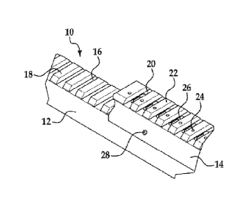
Referring now to FIG. 1, a perspective view of an inductively powering rail
mounted on a MIL-STD- 1913 rail is shown generally as 10.
Feature 12 is a MIL-STD-1913 rail, such as a Weaver rail, NATO STANAG 4694
accessory rail or the like. Sliding over rail 12 is an inductively powering
rail 14. Rail 12
has a plurality of rail slots 16 and rail ribs 18, which are utilized in
receiving an accessory.
An inductively powering rail 14 comprises a plurality of rail slots 20, rail
ribs 22 and pins
24, in a configuration that allows for the mating of accessories with
inductively powering
rail 14. Ills not the intent of the inventors to restrict embodiments to a
specific rail
configuration, as it may be adapted to any rail configuration. The preceding
serves only as
an example of several embodiments to which inductively powering rail 14 may be
mated.
In other embodiments, the inductively powering rail 14 can be mounted to
devices having
apparatus adapted to receive the rail 14.
Pins 24 in one embodiment are stainless steel pins of grade 430. When an
accessory is connected to inductively powering rail 14, pins 24 connect to
magnets 46 and
trigger magnetic switch 48 (see Figure 3) to indicate to the inductively
powering rail 14
that an accessory has been connected. Should an accessory be removed the
connection is
broken and recognized by the system managing inductively powering rail 14 Pins
24 are
offset from the center of inductively powering rail 14 to ensure an accessory'
is mounted in
the correct orientation, for example a laser accessory or flashlight accessory
could not be
mounted backward, and point in the users face as it would be required to
connect to pins
24, to face away from the user of the firearm. Pin hole 28 accepts a cross pin
that locks
and secures the rails 12 and 14 together.
Referring now to FIG. 2, a cross section vertical view of a primacy U-Core and
a
secondary U-Core is shown. Primary U-Core 26 provides inductive power to an
accessory
when connected to inductively powering rail 14. Each of primary U-core 26 and
secondary
7
AMENDED SHEET
PCT/CA2013/050598
CA 02881982 2015-02-13 16
June 2014 16-06-2014
U-core 50 are electromagnets. The wire wrappings 60 and 62 provide an
electromagnetic
field to permit inductive power to be transmitted bi-directionally between
inductively
powering rail 14 and an accessory. Power sources for each primary U-core 26 or
secondary U-core 50 may be provided by a plurality of sources. A power source
may be
within the firearm, it may be within an accessory or it may be provided by a
source such as
a battery pack contained in the uniform of the user that is connected to the
firearm, or by a
super capacitor connected to the system. These serve as examples of diverse
power
sources that may be utilize by embodiments of the invention.
Referring now to FIG. 3, a longitudinal cross section side view of an
accessory
mounted to an inductively powering rail 14; is shown generally as 40.
Accessory 42 in
this example is a lighting accessory, having a forward facing lens 44.
Accessory 42
connects to inductively powering rail 14, through magnets 46 which engage pins
24 and
trigger magnetic switch 48 to establish an electrical connection, via primary
PCB 54, to
inductively powering rail 14.
As shown in FIG. 3, three connections have been established to inductively
powering rail 14 through the use of magnets 46. In addition, three secondary U-
cores 50
connect to three primary U-cores 26 to establish an inductive power source for
accessory
42. To avoid cluttering the Figure, we refer to the connection of secondary U-
core 50 and
primary U-core 26 as an example of one such mating. This connection between U-
cores
50 and 26 allows for the transmission of power to and from the system and the
accessory.
There may be any number of connections between an accessory 42 and an
inductively
powering rail 14, depending upon power requirements. In one embodiment each
slot
provides on the order of two watts. Of course, power transfers greater or less
than two
watts are considered to be within the scope of embodiments disclosed herein.
In both the accessory 42 and the inductively powering rail 14 are embedded
Printed Circuit Boards (PCBs), which contain computer hardware and software to
allow
each to communicate with each other. The PCB for the accessory 42 is shown as
accessory PCB 52. The PCB for the inductively powering rail 14 is shown as
primary
PCB 54. These features are described in detail with reference to FIG. 5 and
FIG. 6.
Referring now to FIG. 4 a block diagram of the components of an inductively
powered rail system is shown generally as 70.
System 70 may be powered by a number of sources, all of which are controlled
by
master controller 72. Hot swap controller 74 serves to monitor and distribute
power
8
AMENDED SHEET
PCT/CA2013/050598
CA 02881982 2015-02-13 16
June 2014 16-06-2014
within system 7. The logic of power distribution is shown in FIG. 9. Hot swap
controller
74 monitors power from multiple sources. The first in one embodiment being one
or more
18.5V batteries 78 contained within the system 70, for example in the stock or
pistol grip
of a firearm. This voltage has been chosen as optimal to deliver two watts to
each
inductively powering rail slot 20 to which an accessory 42 is connected. This
power is
provided through conductive power path 82. A second source is an external
power source
80, for example a power supply carried external to the system by the user. The
user could
connect this source to the system to provide power through conductive power
path 82 to
recharge battery 78. A third source may come from accessories, which may have
their
own auxiliary power source 102, i.e. they have a power source within them.
When
connected to the system, this feature is detected by master CPU 76 and the
power source
102 may be utilized to provide power to other accessories through inductive
power path
90, should it be needed.
Power is distributed either conductively or inductively. These two different
distribution paths are shown as features 82 and 90 respectively. In essence,
conductive
power path 82 powers the inductively powering rail 14 while inductive power
path 90
transfers power between the inductively powering rail 14 and accessories such
as 42.
Master CPU 76 in one embodiment is a Texas Instrument model MSP430F228, a
mixed signal processor, which oversees the management of system 70. Some of
its
functions include detecting when an accessory is connected or disconnected,
determining
the nature of an accessory, managing power usage in the system, and handling
communications between the rail(s), accessories and the user.
Shown in FIG. 4 are three rails. The first being the main inductively powering
rail
14 and side rail units 94 and 96. Any number of rails may be utilized. Side
rail units 94
and 96 are identical in configuration and function identically to inductively
powering rail
unit 14 save that they are mounted on the side of the firearm and have fewer
inductively
powered sail slots 20. Side rail units 94 and 96 communicate with master CPU
76 through
communications bus 110, which also provides a path for conductive power.
Communications are conducted through a control path 86. Thus Master CPU 76 is
connected to inductively powering rail 14 and through rail 14 to the
microcontrollers 98 of
side rails 94 and 96. This connection permits the master CPU 76 to determine
when an
accessory has been connected, when it is disconnected, its power level and
other data that
may be useful to the user, such as GPS feedback or power level of an accessory
or the
9
AMENDED SHEET
PCT/CA2013/050598
CA 02881982 2015-02-13 16
June 2014 16-06-2014
system. Data that may be useful to a user is sent to external data transfer
module 84 and
displayed to the user. In addition data such as current power level, the use
of an accessory
power source and accessory identification may be transferred between
accessories.
Another example would be data indicating the range to a target which could be
communicated to an accessory 42 such as a scope.
Communications may be conducted through an inductive control path 92. Once an
accessory 42, such as an optical scope are connected to the system, it may
communicate
with the master CPU 76 through the use of inductive control paths 92. Once a
connection
has been made between an accessory and an inductively powering rail 14, 94 or
96
communication is established from each rail via frequency modulation on an
inductive
control path 92, through the use of primary U-cores 26 and secondary U-Cores
50.
Accessories such as 42 in turn communicate with master CPU 76 through rails
14, 94 or
96 by load modulation on the inductive control path 92.
By the term frequency modulation the inventors mean Frequency Shift Key
Modulation (FSK). A rail 14, 94, or 96 sends power to an accessory 42, by
turning the
power on and off to the primary U-core 26 and secondary U-core 50. This is
achieved by
applying a frequency on the order of 40kHz. To communicate with an accessory
42
different frequencies may be utilized. By way of example 40kHz and 50kHz may
be used
to represent 0 and 1 respectively. By changing the frequency that the primary
U-cores are
turned on or off information may be sent to an accessory 42. Types of
information that
may be sent by inductive control path 92 may include asking the accessory
information
about itself, telling the accessory to enter low power mode, ask the accessory
to transfer
power. The purpose here is to have a two way communication with an accessory
42.
By the term load modulation the inventors mean monitoring the load on the
system
70. If an accessory 42 decreases or increases the amount of power it requires
then master
CPU 76 will adjust the power requirements as needed.
Accessory 104 serves as an example of an accessory, being a tactical light. It
has
an external power on/off switch 106, which many accessories may have as well
as a safe
start component 108. Safe start component 108 serves to ensure that the
accessory is
properly connected and has appropriate power before turning the accessory on.
Multi button pad 88 may reside on the firearm containing system 70 or it may
reside externally. Multi button pad 88 permits the user to turn accessories on
or off or to
receive specific data, for example the distance to a target or the current GPS
location.
AMENDED SHEET
PCT/CA2013/050598
CA 02881982 2015-02-13 16
June 2014 16-06-2014
Multi-button pad 88 allows a user to access features the system can provide
through
external data transfer module 84.
Referring now to FIG. 5 a block diagram of a primary Printed Circuit Board
(PCB)
contained within an inductively powering rail is shown as feature 54.
Power is received by PCB 54 via conductive power path 82 from master
controller
72 (see FIG. 4). Hot swap controller 74 serves to load the inductively
powering rail 14
slowly. This reduces the amount of in rush current during power up. It also
limits the
amount of current that can be drawn from the inductively powering rail 14.
Conductive
power is distributed to two main components, the inductively powering rail
slots 20 and
the master CPU 76 residing on PCB 54.
Hot swap controller 74 provides via feature 154, voltage in the range of 14V
to
22V which is sent to a MOSFET and transformer circuitry 156 for each
inductively
powering rail slot 20 on inductively powering rail 14.
Feature 158 is a 5V switcher that converts battery power to 5V for the use of
MOSFET drivers 160. MOSFET drivers 160 turn the power on and off to MOSFET and
transformer circuitry 156 which provides the power to each primary U-Core 26.
Feature
162 is a 3.3V Linear Drop Out Regulator (LDO), which receives its power from
5V
switcher 158. LDO 162 provides power to mastel CPU 76 and supporting logic
within
each slot. Supporting logic is Mutiplexer 172 and D Flip Flops 176.
The Multiplexer 172 and the D Flip-Flops 176, 177 are utilized as a serial
shift
register. Any number of multiplexers 172 and D Flip-Flops 176, 177 may be
utilized,
each for one inductively powered rail slot 20. This allows master CPU 76 to
determine
which slots are enabled or disabled and to also enable or disable a slot. The
multiplexer
172 is used to select between shifting the bit from the previous slot or to
provide a slot
enable signal. The first D Flip Flop 176 latches the content of the
Multiplexer 172 and the
second D Flip-Flop 177 latches the value of D Flip-Flop 177 if a decision is
made to
enable or disable a slot.
Hall effect transistor 164 detects when an accessory is connected to
inductively
powering rail 14 and enables MOSFET driver 160.
Referring now to FIG. 6 a block diagram of a PCB contained within an accessory
such as 42 is shown generally as 52 Feature 180 refers to the primary U-Core
26 and the
secondary U-Core 50, establishing a power connection between inductively
powering rail
14 and accessory 42. High power ramp circuitry182 slowly ramps the voltage up
to high
11
AMENDED SHEET
PCT/CA2013/050598
CA 02881982 2015-02-13 16
June 2014 16-06-2014
power load when power is turned on. This is necessary as some accessories such
as those
that utilize XEON bulbs when turned on have low resistance and they draw
excessive
current. High power load 184 is an accessory that draws more than on the order
of two
watts of power.
Full wave rectifier and DC/DC Converter 186 rectifies the power from U-Cores
180 and converts it to a low power load 188, for an accessory such as a night
vision scope.
Pulse shaper 190 clamps the pulse fiam the U-Cores 180 so that it is within
the acceptable
ranges for microcontroller 98 and utilizes FSK via path 192 to provide a
modified pulse to
microcontroller 98 Microcontroller 98 utilizes a Zigbee component 198 via
Universal
Asynchronous Receiver Transmitter component (UART 196) to communicate between
an
accessory 42 and master controller 72. The types of information that may be
communicated would include asking the accessory for information about itself,
instructing
the accessory to enter low power mode or to transfer power.
Referring now to FIG. 7, a block diagram of the components of a master
controller
72 is shown (see FIG. 1) Conductive power is provided from battery 78 via
conductive
power path 82. Hot swap controller 74 slowly connects the load to the
inductively
powering rail 14 to reduce the amount of in rush current during power up. This
also
allows for the limiting of the amount of current that can be drawn. Feature
200 is a 3.3v
DC/DC switcher, which converts the battery voltage to 3.3V to be used by the
master CPU
76.
Current sense circuitry 202 measures the amount of the current being used by
the
system 70 and feeds that information back to the master CPU 76. Master
controller 72
also utilizes a Zi2bee component 204 via Universal Asynchronous Receiver
Transmitter
component (UART) 206 to communicate with accessories connected to the
inductively
powering rail 14, 94 or 96.
Before describing Figures 8, 9 and 10 in detail, we wish the reader to know
that
these Figures are flowcharts or processes that run in parallel, they each have
their own
independent tasks to perform. They may reside on any device but in one
embodiment all
would reside on master CPU 76.
Referring now to Fig 8, a flow chart of the steps of connecting an accessory
to an
inductively powering rail is shown generally as 300. Beginning at step 302,
the main
system power switch is turned on by the user through the use of multi-button
pad 88 or
another switch as selected by the designer. Moving next to step 304 a test is
made to
12
AMENDED SHEET
PCT/CA2013/050598
CA 02881982 2015-02-13 16
June 2014 16-06-2014
determine if an accessory, such as feature 42 of Fig. 4 has been newly
attached to
inductively powering rail 14 and powered on or an existing accessory 42
connected to
inductively powering rail 14 is powered on. At step 306 the magnets 46 on the
accessory
magnetize the pins 24 thereby closing the circuit on the primary PCB 54 via
magnetic
switch 48 and thus allowing the activation of the primary and secondary U-
cores 26 and
50, should they be needed. This connection permits the transmission of power
and
communications between the accessory 42 and the inductively powering rail 14
(see
features 90 and 92 of Fig 4).
Moving now to step 308 a communication link is established between the master
CPU 76 and the accessory via control inductive control path 92. Processing
then moves to
step 310 where a test is made to determine if an accessory has been removed or
powered
off. If not, processing returns to step 304. If so, processing moves to step
312 where
power to the primary and secondary U-Cores 26 and 50 for the accessory that
has been
removed.
Fig 9 is a flow chart of the steps for managing power usage shown generally as
320. There may be a wide range of accessories 42 attached to an inductively
powering rail
14. They range from low powered (1.5 to 2.0 watts) and high powered (greater
than 2.0
watts). Process 320 begins at step 322 where a test is made to determine if
system 70
requires power. This is a test conducted by master CPU 76 to assess if any
part of the
system is underpowered. This is a continually running process. If power is at
an
acceptable level, processing returns to step 322. If the system 70 does
require power,
processing moves to step 324. At step 324 a test is made to determine if there
is an
external power source. If so, processing moves to step 326 where an external
power
source such as 80 (see Fig. 4) is utilized. Processing then returns to step
322. If at step
324 it is found that there is no external power source, processing moves to
step 328. At
step 328 a test is made to determine if there is an auxiliary power source
such as feature
102 (see Fig. 4). If so processing moves to step 330 where the auxiliary power
source is
utilized. Processing then returns to step 322. If at step 328 it is determined
that there is no
auxiliary power source, processing moves to step 332. At step 332 a test is
made to
determine if on board power is available. On board power comprises a power
device
directly connected to the inductively powering rail 14. If such a device is
connected to the
inductively powering rail 14, processing moves to step 334 where the system 70
is
powered by on board power. Processing then returns to step 322. If at step 332
no on
13
AMENDED SHEET
PCT/CA2013/050598
CA 02881982 2015-02-13 16
June 2014 16-06-2014
board power device is located processing moves to step 336. At step 336 a test
is made to
determine if there is available power in accessories. If so, processing moves
to step 338
where power is transferred to the parts of the system requiring power from the
accessories.
Processing then returns to step 322. If the test at step 336 finds there is no
power available,
then the inductively powering rail 14 is shut down at step 340.
The above steps are selected in an order that the designers felt were
reasonable and
logical. That being said, they do not need to be performed in the order cited
nor do they
need to be sequential. They could be performed in parallel to quickly report
back to the
Master CPU 76 the options for power.
Figure 10 is a flow chart of the steps for determining voltage and temperature
of
the system, shown generally as 350. Beginning at step 352 a reading is made of
the power
remaining in battery 78. The power level is then displayed to the user at step
354. This
permits the user to determine if they wish to replace the batteries or
recharge the batteries
from external power source 80. Processing moves next to step 356 where a test
is made
on the voltage. In one embodiment the system 70 utilizes Lithium-Ion
batteries, which
provide near constant voltage until the end of their life, which allows the
system to
determine the decline of the batteries be they battery 78 or batteries within
accessories. If
the voltage is below a determined threshold processing moves to step 358 and
system 70 is
shut down. If at step 356 the voltage is sufficient, processing moves to step
360. At this
step a temperature recorded by a thermal fuse is read. Processing then moves
to step 362,
where a test is conducted to determine if the temperature is below a specific
temperature.
Lithium-Ion batteries will typically not recharge below -5 degrees Celsius. If
it is too cold,
processing moves to step 358 where inductively powering rail 14 is shut down.
If the
temperature is within range, processing returns to step 352.
With regard to communication between devices in system 70 there are three
forms
of communication, control path 86, inductive control path 92 and Zigbee (198,
204).
Control path 86 provides communications between master CPU 76 and inductively
powered rails 14, 94 and 96. Inductive control path 92 provides communication
between
an accessory such as 42 with the inductively powered rails 14, 94 and 96.
There are two
lines of communication here, one between the rails and one between the
accessories,
namely control path 86 and inductive control path 92 Both are bidirectional
The Zigbee
links (198, 204) provide for a third line of communication directly between an
accessory
such as 42 and master CPU 76.
14
AMENDED SHEET
PCT/CA2013/050598
CA 02881982 2015-02-13 16
June 2014 16-06-2014
Referring now to FIGS. 11-191) alternative embodiments of the present
invention
are illustrated. As with the previous embodiments, a rail configuration
designed to mount
accessories such as sights, lasers and tactical lights is provided. In
accordance with an
exemplary embodiment a Networked Powered Data System (NPDS) is provided
wherein
the rail or rails is/are configured to provide power and data through a weapon
coupled to
accessories. Furthermore and in additional embodiments, the power and data may
be
exchanged between the weapon and/or a user coupled to the weapon by a tether
and in
some applications the user is linked a communications network that will allow
data
transfer to other users who may or may not also have weapons with rail
configurations that
are coupled to the communications network.
As used herein rails may refer to inductively powered rails or Networked
Powered
Data System rails. As previously described, the rails will have recoil slots
that provide
data and power as well as mechanically securing the accessory to the rail.
In this embodiment, or with reference to the NPDS rail, specific recoil slots
have
been dedicated for power only while other recoil slots have been configured
for data
communication only. In one non-limiting exemplary embodiment, one of every
three rail
slots is dedicated for data communication and two of every three rail slots
are dedicated to
power transfer. Therefore, every three slots in this embodiment will be
functionality
defined as two power slots and one communications slot. In one non-limiting
configuration, the slots will be defined from one end of the rail and the
sequence will be as
follows: first slot from an end of the rail is dedicated to data, second slot
from the end is
dedicated to power, third slot from the end is dedicated to power, fourth slot
from the end
is dedicated to data, fifth slot from the end is dedicated to power, six slot
from the end is
dedicated to power, etc. Of course, exemplary embodiments of the present
invention
contemplate any variations on the aforementioned sequence of data and power
slots.
Contemplated accessories for use with the NPDS rail would optimally have
either
a 3 slot or 6 slot or longer multiples of power-data sequence to benefit from
interfacing
with power and data slot sequence mentioned above. Accordingly, the accessory
can be
placed at random anywhere on the rail. In this embodiment, the accessory will
have the
capability to discern which recoil slot is dedicated to power and which recoil
slot is
dedicated to data.
AMENDED SHEET
PCT/CA2013/050598
CA 02881982 2015-02-13 16
June 2014 16-06-2014
In contrast, to some of the prior embodiments data and power was provided in
each
slot however and by limiting specific slots to data only higher rates of data
transfer were
obtained.
As illustrated in FIG. 11, a perspective view of an inductively powered NPDS
rail
is shown generally as 410. As in the previous embodiments, an inductively
powering rail
414 is slid over a rail 412 that has a plurality of rail slots 416 and rail
ribs 418.
Alternatively, the rail 414 may be integral with the upper receiver and
replace rail 412.
The inductively powering rail 414 has a plurality of rail slots 420, rail ribs
422 and pins
424, 425. The rail slots and ribs are arranged for mating of accessories with
inductively
powering rail 414. As discussed above, pins 424 are associated with powered
slots "P"
while pins 425 are associated with data slots "D". It is not the intent of the
inventors to
restrict embodiments to a specific rail configuration, as it may be adapted to
any rail
configuration. The preceding serves only as an example of several embodiments
to which
inductively powering rail 414 may be mated.
In one embodiment each slot provides on the order of four watts. Of course,
power
transfers greater or less than four watts are considered to be within the
scope of
embodiments disclosed herein.
Pins 424 and 425 are in one embodiment stainless steel pins of grade 430. Of
course, other alternative materials are contemplated and the embodiments of
the present
invention are not limited to the specific materials mentioned above. Referring
now to
FIGS. 12A and 12B and when an accessory 442 is connected to inductively
powering rail
414, pins 424 and 425 are magnetized by magnets 446 located within each
portion of the
accessory configured to be positioned over the ribs 422 of the rail 414 such
that pins 424
and 425 are magnetized by the magnets 446. As illustrated in FIG. 12A, which
is a cross
sectional view of a portion of an accessory coupled to the rail, each pin 425
is configured
such that a first end 445 is located on top of rib 422, an intermediate
portion 447 of pin
425 is located above magnetic switch 448 and a second end 449 is also located
on rib 422.
Accordingly and when pin 425 is magnetized by magnet 446 in accessory 442 when
the
accessory is placed upon the rail, the magnetized pin 425 causes magnetic
switch 448 to
close to indicate to the inductively powering rail 414 that an accessory has
been connected
to the data slot D.
In addition and in this embodiment, accessory 442 is provided with a magnetic
accessory switch 451 that is also closed by the magnetized pin 425 which now
returns to
16
AMENDED SHEET
PCT/CA2013/050598
CA 02881982 2015-02-13 16
June 2014 16-06-2014
the surface of rib 422. Here, the accessory via a signal from magnetic switch
451 to a
microprocessor resident upon the accessory will be able to determine that the
secondary
coil 450 associated with the switch 451 in FIG. 12A is located above a data
slot D and this
coil will be dedicated to data transfer only via inductive coupling.
Accordingly, the data
recoil slot is different from the power slot in that the associated type 430
stainless steel pin
is extended to become a fabricated clip to conduct the magnetic circuit from
the accessory
to the rail and back again to the accessory. The clip will provide a magnetic
field which,
will activate the solid state switch or other equivalent item located within
the rail on the
one side and then will provide a path for the magnetic field on the other side
of the rail
reaching up to the accessory. Similarly, the accessory will have a solid state
switch or
equivalent item located at each slot position which, will be closed only if it
is in proximity
with the activated magnetic field of the data slot. This provides detection of
the presence
and location of the adjacent data slot. In accordance with various embodiments
disclosed
herein, the accessory circuitry and software is configured to interface with
the rail in terms
of power and data communication.
In contrast and referring to FIG. 12B, which is a cross sectional view of an
another
portion of the accessory secured to the rail, the secondary coil 450
associated with switch
451 of the portion of the accessory illustrated in FIG. 12B will be able to
determine that
the secondary coil 450 associated with the switch 451 in FIG. 12B is located
above a
power slot P and this coil will be dedicated to power transfer only via
inductive coupling.
As mentioned, above the complimentary accessory is configured to have a
secondary coil
450, magnet 446 and switch 451 for each corresponding rib/slot combination of
the rail
they are placed on such that the accessory will be able to determine if it has
been placed
on a data only D of power only P slot/rib combination according to the output
of switch
451.
It being understood that in one alternative embodiment the primary coils
associated
with a rib containing pin 424 or pin 425 (e.g., data or power coils) may in
one non-limiting
embodiment be on either side of the associated rib and accordingly the
secondary coils of
the accessory associated with switch 451 will be located in a corresponding
location on the
accessory. For example, if the data slots are always forward (from a weapon
view) from
the rib having pin 425 then the accessory will be configured to have the
secondary coils
forward from its corresponding switch 451. Of course and in an alternative
configuration,
the configuration could be exactly opposite. It being understood that the ribs
at the end of
17
AMENDED SHEET
PCT/CA2013/050598
CA 02881982 2015-02-13 16
June 2014 16-06-2014
the rail may only have one slot associated with it or the rail itself could
possible end with a
slot instead of a rib.
Still further and in another alternative embodiment, the slots on either side
of the
rib having pin 425 may both be data slots as opposed to a single data slot
wherein a
data/power slot configuration may be as follow's: D, P, P, D, D, ... as
opposed to
...D, P. P. D, P, P ... for the same six slot configurations however, and
depending on the
configuration of the accessory being coupled to the rail a device may now have
two data
slots (e.g., secondary coils on either side of switch 451 that are now
activated for data
transfer). Of course, any one of numerous combinations are contemplated to be
within the
scope of exemplary embodiments of the present invention and the specific
configurations
disclosed herein are merely provided as non-limiting examples.
As in the previous embodiment and should the accessory be removed and the
connection between the accessory and the rail is broken, the change in the
state of the
switch 451 and switch 448 is recognized by the system managing inductively
powering
rail 414. As in the previous embodiment, pins 424 can be offset from the
center of
inductively powering rail 414 to ensure an accessory is mounted in the correct
orientation.
In yet another alternative and referring now to FIG. 12C, a pair of pins 425
are
provided in the data slot and a pair of separate magnets (accessory magnet and
rail magnet
are used). Here the pins are separated from each other and one pin 425,
illustrated on the
right side of the FIG., is associated with the accessory magnet 446 and rail
switch 448
similar to the FIG. 12A embodiment however, the other pin 425 illustrated on
the left side
of the FIG., is associated with the accessory switch 451 and a separate rail
magnet 453,
now located in the rail. Operation of accessory switch 451 and rail switch 448
are similar
to the previous embodiments.
Power for each primary 426 or secondary 450 can be provided by a plurality of
sources. For example, a power source may be within the firearm, it may be
within an
accessory or it may be provided by a source such as a battery pack contained
in the
uniform of the user that is connected to the firearm, or by a super capacitor
connected to
the system. The aforementioned serve merely as examples of diverse power
sources that
may be utilize by embodiments of the invention.
Although illustrated for use in inductive coupling of power and/or data to and
from
an accessory to the rail, the pin(s), magnet(s) and associated switches and
arrangements
thereof will have applicability in any type of power and data transfer
arrangement or
18
AMENDED SHEET
PCT/CA2013/050598
CA 02881982 2015-02-13 16
June 2014 16-06-2014
configurations thereof (e.g., non-inductive, capacitive, conductive, or
equivalents thereof,
etc.).
Aside from the inductive power transferring, distributing and managing
capabilities, the NPDS also has bidirectional data communication capabilities.
As will be
further discussed herein data communication is further defined as low speed
communication, medium speed communication and high speed communication. Each
of
which according to the various embodiments disclosed herein may be used
exclusively or
in combination with the other rates/means of data communication. Thus, there
are at least
three data transfer rates and numerous combinations thereof, which are also
referred to as
data channels that are supported by the system and defined by their peak rates
of 100kb/s,
10Mb/s and 500Mb/s. Of course, other data rates are contemplated and exemplary
embodiments are not specifically limited to the data rates disclosed herein.
The three data
channels are relatively independent and can transfer data at the same time.
The three data
channels transfer data in a serial bit by bit manner and use dedicated
hardware to
implement this functionality.
The 100kb/s data channel, also called the low-speed data communication
channel,
is distributed within the system electrically and inductively. Similarly to
the inductive
power transfer, the low speed channel is transferred inductively by modulating
a magnetic
field across an air gap on the magnetic flux path, from the rail to the
accessory and back.
The data transfer is almost not affected by the gap size. This makes the
communication
channel very robust and tolerant to dirt or misalignment. This channel is the
NPDS control
plane. It is used to control the different accessories and transfer low speed
data between
the NPDS microprocessors and the accessories. One slot of every three rail
slots is
dedicated to the low speed communication channel.
The 10Mb/s data channel, also called the medium-speed data communication
channel, is distributed within the system electrically and inductively. It is
sharing
communication rail slots with the low speed data channels and the data is
transferred to the
accessories inductively in the same manner. The NPDS is providing the medium
speed
data channel path from one accessory to another accessory or a soldier tether
coupled to
the rail, and as it does not terminate at the Master Control Unit (MCU) this
allows
simultaneous low speed and medium speed communications on the NPDS system. The
MCU is capable of switching medium speed communications data from one
accessory to
another accessory. When the communication slot is in medium speed mode then
all of the
19
AMENDED SHEET
PCT/CA2013/050598
CA 02881982 2015-02-13 16
June 2014 16-06-2014
related circuit works at a higher frequency and uses different transmission
path within the
system. The low or medium speed communication channel functionality can be
selected
dynamically.
The 500Mb/s data channel, also called the high-speed data communication
channel, is distributed within the system electrically and optically. It is
using a dedicated
optical data port at the beginning of the rail (e.g., closest to the pistol
grip). The high-
speed data channel is transferred optically between optical data port and the
accessories.
Similarly to the medium speed channel, NPDS is providing the high-speed data
channel
path from an accessory to the soldier tether, and as it does not terminate at
the Master
Control Unit (MCU) this allows simultaneous low speed, medium speed and high
speed
communications on the NPDS system.
FIGS. 13A and 13B illustrate a front end of an upper receiver 471 showing an
upper inductive/data rail 414 and side accessory inductive/data rails 494 and
496 wherein
the side accessory inductive/data rails 494 and 496 are directly wired to
upper
inductive/data rail 414 via wires 486 and 482 that are located within bridges
487 fixedly
secured to the upper receiver so that wires 486 and 482 are isolated and
protected from the
elements. Thus, the bridges provide a conduit of power 482 and data 486 from
the top rail
to the side rails (or even a bottom rail not shown). Bridges 487 are
configured to engage
complimentary securement features 491 located on rails 414, 494 and 496 or
alternatively
upper receiver 471 or a combination thereof. In addition, the bridges will
also act as a heat
dissipater. In one embodiment, the bridges are located towards the end of the
rail closest
to the user. The gun barrel is removed from this view for clarity purposes.
FIGS. 13C and
D illustrate alternative configurations of the rail bridges 487 illustrated in
FIGS. 13A and
13B.
FIG. 14A is atop view of the upper receiver 471 with the upper inductive/data
rail
414 and side accessory inductive/data rails 494 and 496 while FIG. 14B is a
top view of
the upper receiver 471 with the upper inductive/data rail 414 and side
accessory
inductive/data rails 494 and 496 without the upper receiver. FIGS. 14C and 14D
illustrate
alternative configurations of the rail bridges 487 and the rail 494
illustrated in FIGS. 14A
and 14B.
Referring now to FIGS. 15A-15B an apparatus and method for securing and
positively locking the inductive/data rail (e.g., upper, side or bottom) to
the existing rail
412 of the upper receiver 471. Here, an expanding wedge feature 491 comprising
a pair of
AMENDED SHEET
PcT/cA2013/050598
CA 02881982 2015-02-13 16
June 2014 16-06-2014
wedge members 493 is provided. To secure rail 414 to rail 412 each wedge
member is
slid into a slot of the rail axially until they contact each other and the
sliding contact
causes the surface of the wedge members to engage a surface of the slot. In
order to
axially insert the wedge members, a pair of complimentary securement screws
495 are
used to provide the axial insertion force as they are inserted into the rail
by engaging a
complimentary threaded opening of the rail 414, wherein they contact and
axially slide the
wedge members 493 as the screw is inserted into the threaded opening.
Referring now to FIGS. 15D-F, alternative non-limiting configurations of
bridges
487 are illustrated. in this embodiment, bridges 487 are attached to the rails
by a
mechanical means such as screws or any other equivalent device.
With reference now to FIG. 16, as discussed generally above the accessories 42
and the master CPU 76 can communicate with one another in several different
manners.
For example, and as also described above, the master CPU 76 can vary the
frequency that
power or another signal is provided to the accessories 42 to provide
information (data) to
them. Similarly, the accessories 42 can communicate data to the master CPU 76
by
utilizing load modulation. As discussed above, such communication can occur on
the
same cores (referred to below as "core pairs") as are used to provide power or
can occur
on separate coils. Indeed, as described above, in one embodiment, one in every
three coils
is dedicated to data transmission.
FIG. 16 illustrates three different communication channels shown as a low
speed
channel 502, a medium speed channel 504 and a high speed channel 506. The low
speed
channel 502 extends from and allows communication between the master CPU 76
and any
of the accessories 42. The low speed channel 502 can be driven by a low speed
transmitter/receiver 510 in the master CPU 76 that includes selection logic
512 for
selecting which of the accessories 42 to route the communication to.
Each accessory 42 includes low speed decoding/encoding logic 514 to receive
and
decode information received over the low speed channel 502. Of course, the low
speed
decoding/encoding logic 514 can also include the ability to transmit
information from the
accessories 42 as described above.
In one embodiment, the low speed channel 502 carries data at or about 100
kB/s.
Of course, other speeds could be used. The low speed channel 502 passes
through an
inductive coil pair 520 (previously identified as primary coil 26 and
secondary coil 50
hereinafter referred to as inductive coil pair 520) between each accessory 42
and the
21
AMENDED SHEET
PCT/CA2013/050598
CA 02881982 2015-02-13 16
June 2014 16-06-2014
master CPU 76. It shall be understood, however, that the inductive coil pair
could be
replaced include a two or more core portions about which the coil pair is
wound. In
another embodiment, the cores can be omitted and the inductive coil pair can
be
implemented as an air core transformer. As illustrated, the inductive coil
pairs 520 are
contained within the inductive powering rail 14. Of course and as illustrated
in the
previous embodiments, one or more of the coils included in the inductive coil
pairs 520
can be displaced from the inductive powering rail 14.
The medium speed channel 504 is connected to the inductive coil pairs 520 and
shares them with low speed channel 502. For clarity, branches of the medium
speed
channel 504 as illustrated in dashed lines. As one of ordinary skill will
realize, data can be
transferred on both the low speed channel 502 and the medium speed channel at
the same
time. The medium speed channel 504 is used to transmit data between the
accessories 42.
Both the low and medium speed channels 502, 504 can also be used to transmit
data to or receive data from an accessory (e.g. a tether) not physically
attached to the
inductively powering rail 14 as illustrated by element 540. The connection
between the
master CPU 76 can be either direct or through an optional inductive coil pair
520'. In one
embodiment, the optional inductive coil pair 520' couples power or data or
both to a CPU
located in or near a handle portion of a gun.
To allow for communication between accessories over the medium speed channel
504, the master CPU 76 can include routing logic 522 that couples signals from
one
accessory to another based on information either received on the medium speed
channel
504. Of course, in the case where two accessories coupled to the inductively
powering rail
14 are communicating via the medium speed channel 502, the signal can be
boosted or
otherwise powered to ensure is can drive the inductive coil pairs 520 between
the
accessories.
In another example, the accessory that is transmitting the data first utilizes
the low
speed channel 502 to cause the master CPU 76 to set the routing logic 522 to
couple the
medium speed channel 504 to the desired receiving accessory. Of course, the
master CPU
76 itself (or an element coupled to it) can be used to separate low and medium
speed
communications from one another and provide them to either the low speed
transmitter/receiver 510 or the routing logic 522, respectively. In one
embodiment, the
medium speed channel 504 carries data at 10 MB/s.
22
AMENDED SHEET
PCT/CA2013/050598
CA 02881982 2015-02-13 16
June 2014 16-06-2014
FIG. 16 also illustrates a high speed channel 506. In one embodiment, the high
speed channel 506 is formed by an optical data line and runs along at least a
portion of the
length of the inductively powering rail 14. For clarity, however, the high
speed channel
506 is illustrated separated from the inductively powering rail 14.
Accessories 42 can
include optical transmitter/receivers 542 for providing signals to and
receiving signals
from the high speed channel 506. In one embodiment, a high speed signal
controller 532
is provided to control data flow along the high speed channel 506. It shall be
understood
that the high speed signal controller 532 can be located in any location and
may be
provided, for example, as part of the master CPU 76. In one embodiment, the
high speed
signal controller 532 is an optical signal controller such as, for example, an
optical router.
FIG. 17 illustrates an example of the MOSFET driver 154 coupled to MOSFET
and transformer circuitry 156. In general, the MOSFET driver 154 the MOSFET
and
transformer circuitry 156 to produce an alternating current (AC) output at an
output coil
710. The AC output couples power to a receiving coil 712. As such, the output
coil 710
and the receiving coil 712 form an inductive coil pair 520. In one embodiment,
the
receiving coil 712 is located in an accessory as described above.
It shall be understood that it is desirable to achieve efficient power
transfer from
the output coil 710 to the receiving coil 712 (or vice versa). Utilizing the
configuration
shown in FIG. 17 has led, in some instances, to a power transfer efficiency of
greater than
90%. In addition, it shall be understood, that the accessory could also
include such a
configuration to allow for power transfer from the receiving coil 712 to the
output coil
710. The illustrated MOSFET and transformer circuitry 156 includes an LLC
circuit 711
that, in combination with the input and output coils, forms an LLC resonant
converter.
The LLC circuit 711 includes, as illustrated, a leakage inductor 706, a
magnetizing
inductor 708 and a capacitor 714 serially connected between input node 740 and
ground.
The magnetizing inductor 708 is coupled in parallel with the output coil 710.
The
operation and location of the first and second driving MOSFET's 702, 704 is
well known
in the art and not discussed further herein. In one embodiment, utilizing an
LLC resonant
converter as illustrated in FIG. 17 can lead to increased proximity effect
losses due to the
higher switching frequency, fringe effect losses due to the presence of a gap,
an effective
reverse power transfer topology, and additional protection circuits due to the
unique nature
of the topology.
23
AMENDED SHEET
PcT/cA2013/050598
CA 02881982 2015-02-13 16
June 2014 16-06-2014
In one embodiment, the MOSFET's 702, 704 are switched at the second resonant
frequency of the resonant LLC resonant converter. In such a case, the output
voltage
provided at the output coil 710 is independent of load. Further, because the
second
resonant frequency is dominated by the leakage inductance and not the
magnetizing
inductance, it also means that changes in the gap size (g) do little to change
the second
resonant point. As is known in the art, if the LLC resonant converter is above
the second
resonant point, reverse recovery losses in rectifying diodes in the receiving
device (not
illustrated) are eliminated as the current through the diode goes to zero when
they are
turned off. If operated below the resonant frequency, the RMS currents are
lower and
conduction losses can be reduced which would be ideal for pure resistive loads
(i.e.: flash
light). However, operating either above or below the second resonant point
lowers the
open loop regulation, so, in one embodiment, it may be desirable to operate as
close as
possible to the second resonant point when power a purely resistive load
(e.g., light bulb)
or rectified load (LED).
The physical size limitations of the application can lead to forcing the
resonant
capacitor 714 to be small. Thus, the LLC resonant converter can require a high
resonant
frequency (e.g., 300 kHz or higher). Increased frequency, of course, leads to
increased
gate drive loss at the MOSFET's 702, 704. To reduce these effects, litz wire
can be used
to connect the elements forming the LLC circuit 711 and in the coils 710, 712.
In
addition, it has been found that utilizing litz wire in such a manner can
increase gap
tolerance.
The increased gap tolerance, however, can increase fringe flux. Fringe flux
from
the gap between the cores around which coils 710 and 712 are wound can induce
conduction losses in metal to the cores. Using litz wire can combat the loss
induced in the
windings. However, a means of reducing the loss induced in the rails is
desirable. This
can be achieved by keeping the gap away from the inductively coupling rail,
creating a
gap spacer with a distributed air gap that has enough permeability to prevent
flux fringing,
or by adding magnetic inserts into the rail to prevent the flux from reaching
the aluminum.
Referring now to FIG. 18, portions of an upper receiver and a lower receiver
equipped with the inductive power and data transferring rail are illustrated.
As illustrated,
the pistol grip 897 is configured to have a rear connector 899 configured for
a sling tether
501 to transmit power and bi-directional data from an external soldier system
540 coupled
to the tether.
24
AMENDED SHEET
PCT/CA2013/050598
CA 02881982 2015-02-13 16
June 2014 16-06-2014
As illustrated, the pistol grip is configured to support the rear power/data
connector
for the sling tether. In addition, a portion 905 of the pistol grip is
reconfigured to wrap up
around the top of the upper receiver to provide a supporting surface for
buttons 907 to
control (on/off, etc.) the accessories mounted on the rails. In one
embodiment, the buttons
will also be provided with haptic features to indicate the status of the
button or switch
(e.g., the buttons will vibrate when depressed).
Portion 905 also includes a pair of coils 909 for inductively coupling with
another
pair of coils on the lower receiver (not shown). In one non-limiting exemplary
embodiment, the inductive cores will be an EQ20/R core commercially available
from
Ferroxcube. Further information is available at the following website
http://www.ferroxcube.com/prod/assets/eq20r.pdfand in particular figure 1
found at the
aforementioned website. A circuit board will have a coil pattern and the
EQ20/Rcores will
be cut into the middle of the circuit board.
Accordingly, portion 905 provides a means for coupling between the upper and
lower receiver to transmit power and data to and from the rails. As such, data
from a
microprocessor or other equivalent device resident upon the upper receiver can
be
transferred to a microprocessor or other equivalent device resident upon the
lower
receiver. In addition, power may be transferred between the upper receiver and
lower
receiver via inductive coupling. FIGS. 19A-191) illustrate views of portion
905 for
coupling the upper receiver portion to the lower receiver wherein the coupling
has features
911 for receipt of the cores therein.
In addition and referring now to FIG. 18 one of the optical
transmitters/receivers
542 is located at the rear portion of the rail for optical communication with
a
complimentary optical transmitter/receiver 542 located on the accessory (See
at least FIG.
16). As illustrated, the optical transmitter/receiver 542 is coupled to a
fiber optic wire or
other data communication channel 506 that is coupled to another optical
transmitter/receiver 542' that communicates with an optical
transmitter/receiver 542'
located on the lower receiver and is coupled to the rear connector 899 via a
fiber optic
wire or other data communication channel 506 located within the lower
receiver.
Accordingly and as illustrated schematically in at least FIGS. 16 and 18 is
that
portion 905 allows data and power transfer between the upper receiver and the
lower
receiver via the coils of the upper receiver and the lower receiver while also
allowing the
upper receiver to be removed from the lower receiver without physically
disconnecting a
AMENDED SHEET
PCT/CA2013/050598
CA 02881982 2015-02-13 16
June 2014 16-06-2014
wire connection between the upper and lower receiver. Similarly and in the
embodiment
where the high speed channel is implemented the optical transmitter/receivers
542' allow
the upper receiver to be removed from the lower receiver without physically
disconnecting
a wire connection between the upper and lower receiver. Also shown in FIG 18
is that a
rear sight 919 is provided at the back of the NPDS rail.
Referring now to FIGS. 18A and 20A-F, an alternative configuration of portion
905, illustrated as 905', is provided. As mentioned above, portion 905'
provides a means
for providing the inductive method of bi-directionally transferring power and
data from
the upper receiver to the lower receiver. In this embodiment, 905' is an
appendage of the
upper receiver. Portion 905' has a housing configured to receive a circuit
board 921 and
associated electronics required for data and power communication. Once the
circuit board
921 is inserted therein it is covered by a cover 923. In one embodiment, cover
923 is
secured to the housing of portion 905' by a plurality of screws 925. Of
course, any
suitable means of securement is contemplated to be within the scope of
exemplary
embodiments of the present invention.
In this embodiment, portion 905'is configured to have a power core 927 and a
pair
of data cores 929. As illustrated, the power core 927 is larger than the
smaller two data
cores 929. Portion 905'is configured to interface with the pistol grip 897
such that as the
two are aligned, portion 905' locks or wedges into complementary features of
the pistol
grip 897 such that the pistol grip is secured thereto and the power and data
cores (927 and
929) are aligned with complementary power and data cores located in the pistol
grip 897.
Accordingly and in this embodiment, the pistol grip 897 will also have a pair
of data cores
and a power core matching the configuration of those in portion 905'.
In this embodiment, the smaller data cores 929 and those of the pistol grip
can be
configured for low speed data (100kbps) and medium speed data (10 Mbps) at the
same
time. Of course, the aforementioned data transfer rates are merely provided as
examples
and exemplary embodiments of the present invention contemplate ranges greater
or less
than the aforementioned values.
FIG. 21 illustrates a portion of a pistol grip 897 contemplated for use with
portion
905'. As illustrated, a pair of complementary data cores 931 and a
complimentary power
core 933 are configured and positioned to be aligned with portion 905'and its
complementary cores (data and power) when portion 905' is secured to pistol
grip 897
such that inductive power and data transfer can be achieved. In one non-
limiting
26
AMENDED SHEET
PCT/CA2013/050598
CA 02881982 2015-02-13 16
June 2014 16-06-2014
embodiment, pistol grip 897 has a feature 935 configured to engage a portion
of portion
905'wherein feature 935 is configured to assist with the alignment and
securement of
portion 905'to the pistol grip 897.
Referring now to FIGS. 22 and 23 yet another alternative method of bi-
directionally transferring power and data from the upper receiver to the lower
receiver is
illustrated. In this embodiment, conductive data and power transmission is
achieved
through a connector such as a cylindrical connector 936. In this embodiment, a
generic
connector 936 (comprising in one embodiment a male and female coupling)
couples a
conduit or cable 937 (illustrated by the dashed lines in FIG. 22) of the upper
receiver to a
complementary conduit or cable 939 of the lower receiver (also illustrated by
dashed lines
in FIG. 22), when the upper receiver is secured to the lower receiver. One non-
limiting
embodiment of such a connector is available from Tyco Electronics.
In order to provide this feature the upper receiver is configured to have an
appendage 941 that provides a passage for the cable 937 from the upper rail to
the joining
cylindrical connector 936. Similar to portion 905 and 905' the appendage 941
is
configured to lock and secure the pistol grip 897 to the upper receiver to
align both halves
of the cylindrical connector 936 (e.g., insertion of male/female pins into
each other).
In this embodiment, the sling attaching plate 938 of the lower receiver
portion has
a common screw 940 to secure the pistol grip to the upper receiver to ensure
alignment of
both halves of the cylindrical connector.
Also shown is a control button 942 (for control on/off, etc. of various
accessories
mounted on the rails or any combination thereof) that is positioned on both
sides the pistol
grip 897. In one non-limiting embodiment, the control button is configured to
act as a
switch for a laser accessory mounted to the weapon. The control button is
found in both
the conductive and inductive pistol grip configurations and is activated by
the side of an
operator's thumb. Requiring side activation by a user's thumb prevents
inadvertent
activation of the control button when handling the grip 897. In other words,
control button
942 requires a deliberate side action of the thumb to press the control button
942.
In order to provide a means for turning on/off the entire system of the NPDS
or the
power supply coupled thereto an on/off button or switch 943 is also located on
the pistol
grip 897.
In addition and referring now to FIG. 24, a power pack or battery 945 is shown
attached to pistol grip 897. In this embodiment, the battery is coupled to the
pistol grip
27
AMENDED SHEET
PCT/CA2013/050598
CA 02881982 2015-02-13 16
June 2014 16-06-2014
using a conductive attachment similar to the one used for power and data
transfer between
the upper receiver and the lower receiver via a generic connector (e.g.,
male/female
configuration). Again, one non-limiting example of such a connector is
available from
Tyco Electronics and could be a similar type connector used in the embodiment
of FIGS.
22 and 23. In order to release the battery pack 945 an actuating lever 947 is
provided.
FIG. 25 shows an alternative method of fastening a battery pack to the bottom
of
the pistol grip 897 as well as an alternative method for transferring
power/data inductively
and bi-directionally. This method uses a power/data rail section 949 that is
mounted to the
bottom of the pistol grip 897, which in one exemplary embodiment is similar in
configuration to the rails used for the upper and lower receivers and
accordingly, it is now
possible to use the same battery pack at the pistol grip location or at a rail
section
elsewhere and accordingly, power the system. In addition, the mounting to the
bottom of
the pistol grip it is also contemplated that the rail can be used to
inductively couple the
battery pack to the pistol grip as any other side as long as a desired
location of the battery
pack is achieved.
In addition and since battery pack can be mounted at the pistol grip location
or a
rail section elsewhere on the weapon, it is now possible to transmitting data
to control the
battery pack mounted anywhere on the weapon or its associated systems. Such
data can
be used to control the power supply and the data as well as power, can be
inductively
transmitted between the battery pack or power supply and the component it is
coupled to.
Accordingly, the controller or central processing unit of the Network Powered
Data
System (NPDS) can determine and choose which battery pack would be activated
first (in
the case of multiple battery pack secured to the system) based upon
preconfigured
operating protocol resident upon the controller. For example and in one non-
limiting
embodiment, the forward rail mounted battery pack would be activated first.
For example and referring now to FIG. 26, a non-limiting example of a power
system 951 for the Network Powered Data System (NPDS) according to an
embodiment
of the present invention is illustrated schematically. Here and as illustrated
in the previous
FIGS. a primary battery pack 945 is secured and coupled to the pistol grip 897
while a
secondary power source or battery pack illustrated as 953 is secured to a
forward rail of
the upper receiver or, of course, any other rail of the weapon. In this
embodiment, the
secondary battery pack 953 can be a stand alone power supply similar to
battery pack 945
or integrated with an accessory mounted to the rail. In one embodiment,
secondary battery
28
AMENDED SHEET
PCT/CA2013/050598
CA 02881982 2015-02-13 16
June 2014 16-06-2014
pack 953 is of the same size and configuration of primary battery pack 945 or
alternatively
may have a smaller profile depending on the desired location on the weapon.
Secondary
battery pack 953 can be utilized in a similar fashion as the primary battery
pack 945 due to
the reversible power capability of the rails as discussed above.
Still further, yet another source of power 955 also controlled by the system
may be
resident upon a user of the weapon (e.g., power supply located in a back pack
of a user of
the weapon) wherein an external power/data coupling is provided via coupling
957 located
at the rear of the pistol grip 897 (See at least FIGS. 21-23). In all cases
both power and
data are transmitted as the master control unit (MCU) of the NPDS communicates
with the
power sources (e.g., primary 945, secondary 953 and external 955) and thus the
MCU
controls all the power supplies of the power system.
One advantage is that the system will work without interruption if for
example, the
primary battery pack 945 is damaged or suddenly removed from pistol grip 897
or rail 414
as long as an alternative power connection (e.g., 953, 955) is active.
Connection of the
primary battery pack 945 or other power source device will also ensure that
the rails are
powered if the pistol grip 897 is damaged or completely missing including the
CPU. For
example and in one implementation, the default configuration of the rails will
be to turn
power on as an emergency mode.
Referring now to FIGS. 27A-45, various alternative exemplary embodiments of
the
present invention are illustrated. As with the previous embodiments, a rail
configuration
designed to mount accessories such as sights, lasers and tactical lights is
provided. As
mentioned above and in accordance with an exemplary embodiment a Networked
Powered
Data System (NPDS) is provided wherein the rail or rails is/are configured to
provide
power and data through a weapon coupled to accessories. Furthermore and in
additional
embodiments, the power and data may be exchanged between the weapon and/or a
user
coupled to the weapon by a tether and in some applications the user is linked
a
communications network that will allow data transfer to other users who may or
may not
also have weapons with rail configurations that are coupled to the
communications
network.
In this embodiment, the conductively powering rail 1014 similar to the above
embodiments comprises a plurality of rail slots 1020, rail ribs 1022 and pins
1024, in a
configuration that allows for the mating of accessories with conductively
powering rail
1014. However power and data transfer is facilitated by a conductive
connection or
29
AMENDED SHEET
PCT/CA2013/050598
CA 02881982 2015-02-13 16
June 2014 16-06-2014
coupling via power and data pins 1015 embedded into the rail 1014 and power
and data
pins 1017 embedded into an accessory 1042.
It is not the intent of the inventors to restrict embodiments to a specific
rail
configuration, as it may be adapted to any rail configuration. The preceding
serves only as
an example of several embodiments to which the conductively powering rail 1014
may be
mated.
Pins 1024 and 1025 in one embodiment are stainless steel pins of grade 430 and
have configurations similar to those illustrated in the cross-sectional views
illustrated in
FIGS. 28A and 28B. When an accessory is connected to conductively powering
rail
1014, pins 1024, 1025 connect to magnets 1046, 1047 and trigger magnetic
switch 1048,
1051 (see FIGS. 28A-28C) to indicate to the conductively powering rail 1014
that an
accessory 1042 has been connected.
Pins 1024 are offset from the center of conductively powering rail 1014 to
ensure
an accessory is mounted in the correct orientation, for example a laser
accessory or
flashlight accessory could not be mounted backward, and point in the users
face as it
would be required to connect to pins 1024, to face away from the user of the
firearm.
Referring now to FIGS. 28A and 28B and when an accessory 1042 is connected to
conductively powering rail 1014, pins 1024 and 1025 are magnetized by magnets
1046
located within each portion of the accessory configured to be positioned over
the ribs 1022
of the rail 1014 such that pins 1024 and 1025 are magnetized by the magnets
1046. As
illustrated in FIG. 28A, which is a cross sectional view of a portion of an
accessory
coupled to the rail, each pin 1025 is configured such that a first end 1045 is
located on top
of rib 1022, an intermediate portion 1047 of pin 1025 is located above
magnetic switch
1048 and a second end 1049 is also located on rib 1022. Accordingly and when
pin 1025
is magnetized by magnet 1046 in accessory 1042 when the accessory is placed
upon the
rail, the magnetized pin 1025 causes magnetic switch 1048 to close to indicate
to the
conductively powering rail 1014 that an accessory has been connected to the
data slot D.
In addition and in this embodiment, accessory 1042 is provided with a magnetic
accessory switch 1051 that is also closed by the magnetized pin 1025 which now
returns to
the surface of rib 1022. Here, the accessory via a signal from magnetic switch
1051 to a
microprocessor resident upon the accessory will be able to determine that the
accessory
electronics 1053 associated with the switch 1051 in FIG. 28A is located above
a data slot
D and these electronics or equivalent items will be dedicated to data transfer
only via
AMENDED SHEET
PCT/CA2013/050598
CA 02881982 2015-02-13 16
June 2014 16-06-2014
conductive coupling. Accordingly, the data slot is different from the power
slot in that the
associated type 430 stainless steel pin is extended to become a fabricated
clip to conduct
the magnetic circuit from the accessory to the rail and back again to the
accessory. The
clip will provide a magnetic field which, will activate the solid state switch
or other
equivalent item located within the rail on the one side and then will provide
a path for the
magnetic field on the other side of the rail reaching up to the accessory.
Similarly, the
accessory will have a solid state switch or equivalent item located at each
slot position
which, will be closed only if it is in proximity with the activated magnetic
field of the data
slot. This provides detection of the presence and location of the adjacent
data slot. In
accordance with various embodiments disclosed herein, the accessory circuitry
and
software is configured to interface with the rail in terms of power and data
communication.
In contrast and referring to FIG. 28B, which is a cross sectional view of an
another
portion of the accessory secured to the rail, the accessory electronics or
other equivalent
item 1053 associated with switch 1051 of the portion of the accessory
illustrated in FIG.
28B will be able to determine that the accessory electronics 1053 associated
with the
switch 1051 in FIG. 28B is located above a power slot P and these electronics
or
equivalent items will be dedicated to power transfer only via conductive
coupling. As
mentioned, above the complimentary accessory may alternatively be configured
to have a
secondary electronics or equivalent item 1053, magnet 1046 and switch 1051 for
each
corresponding rib/slot combination of the rail they are placed on such that
the accessory
will be able to determine if it has been placed on a data only D of power only
P slot/rib
combination according to the output of switch 1051.
It being understood that in one alternative embodiment the electronics
associated
with a rib containing pin 1024 or pin 1025 (e.g., data or power) may in one
non-limiting
embodiment be on either side of the associated rib and accordingly the
electronics or
equivalent item of the accessory associated with switch 1051 will be located
in a
corresponding location on the accessory. For example, if the data slots are
always forward
(from a weapon view) from the rib having pin 1025 then the accessory will be
configured
to have the corresponding electronics forward from its corresponding switch
1051. Of
course and in an alternative configuration, the configuration could be exactly
opposite. It
being understood that the ribs at the end of the rail may only have one slot
associated with
it or the rail itself could possible end with a slot instead of a rib.
31
AMENDED SHEET
PCT/CA2013/050598
CA 02881982 2015-02-13 16
June 2014 16-06-2014
Still further and in another alternative embodiment, the slots on either side
of the
rib having pin 1025 may both be data slots as opposed to a single data slot
wherein a
data/power slot configuration may be as follows: ....D, D, P, P, D, D, ... as
opposed to
...D, P, P, D, P, P ... for the same six slot configurations however, and
depending on the
configuration of the accessory being coupled to the rail a device may now have
two data
slots (e.g., secondary electronics on either side of switch 1051 that are now
activated for
data transfer). Of course, any one of numerous combinations are contemplated
to be
within the scope of exemplary embodiments of the present invention and the
specific
configurations disclosed herein are merely provided as non-limiting examples.
As in the previous embodiment and should the accessory be removed and the
connection between the accessory and the rail is broken, the change in the
state of the
switch 1051 and switch 1048 is recognized by the system managing conductively
powering rail 1014. As in the previous embodiment, pins 1024 can be offset
from the
center of conductively powering rail 1014 to ensure an accessory is mounted in
the correct
orientation.
In yet another alternative and referring now to FIG. 28C, a pair of pins 1025
are
provided in the data slot and a pair of separate magnets (accessory magnet and
rail magnet
are used). Here the pins are separated from each other and one pin 1025,
illustrated on the
right side of the FIG., is associated with the accessory magnet 1046 and rail
switch 1048
similar to the FIG. 28A embodiment however, the other pin 1025 illustrated on
the left
side of the FIG., is associated with the accessory switch 1051 and a separate
rail magnet
1053, now located in the rail. Operation of accessory switch 1051 and rail
switch 1048 are
similar to the previous embodiments.
In this embodiment power and data to and from the accessory is provided by a
plurality of power and data pins or contacts 1015 embedded into the rail 1014
and power
and data pins or contacts 1017 embedded into an accessory 1042. Accordingly, a
galvanically coupled conductive rail power and communication distribution
method for
the rail system is provided.
In one embodiment, the exposed conductive metal rail contacts or contact
surfaces
1035 and 1037 of pins 1015 and 1017 are made of Tungsten Carbide for excellent
durability and corrosion resistance to most environmental elements. In one
embodiment,
the contact surfaces are round pads, pressed against each other to make good
galvanic
contact. The pads, both in the rail and the accessory, are permanently bonded
to short
32
AMENDED SHEET
PCT/CA2013/050598
CA 02881982 2015-02-13 16
June 2014 16-06-2014
posts of copper or other metal, that in turn, are electrically bonded to PCB
substrates, rigid
in the rail and flex in the accessory so that there is some give when the two
surfaces are
brought together. Accordingly, at least one of the pads in each contact pair
provides some
mechanical compliance, and in one embodiment the accessory is the item that
have the
mechanical compliance. Of course, this could also be in the rail or both.
In one embodiment and as illustrated in at least FIGS. 29A-40 the pin/pad
assemblies use an X-section ring 1019 as a seal and compressible bearing 1021,
with the
internal connection end attached to a flex PCB. The pin/pad construction is
shown in at
least FIG. 33. The tungsten carbide pads provide durability where the extreme
G-forces of
weapon firing vibrate the accessory attachment structure. The hardness of the
touching
contact surfaces ensures that little if any abrasion will take place as the
surfaces slip
minutely against each other. The pressure of the seal bearing (x-ring) will
keep the pads
firmly pressed together during the firing vibration, keeping electrical
chatter of the
contacts at minimal levels.
As illustrated and in one embodiment, the slot contacts are composed of small
tungsten "pucks" that are press-fit or brazed to a metal pin. Tungsten carbide
exhibits a
conductivity of roughly 5-10% that of copper and is considered a practical
conductor. Assuming a good electrical bond between the puck and the pin,
resistance
introduced into the power path, accounting two traversals per round trip
(Positive and
Negative contacts). Alternatively, the pins are coated with tungsten carbide.
In yet
another alternative non-limiting embodiment the pins are coated with a
tungsten
composite, which in one non-limiting embodiment may be a nano coat blend of
primarily
tungsten and other materials such as cobalt which will exhibit similar or
superior
properties to tungsten carbide.
FIG. 34 illustrates the rail side pins and caps installed in the rail at each
slot
position. FIG. 35 also illustrates a rail side pin.
Non-limiting examples of suitable copper alloys for the pins are provided as
follows: Copper Alloy 99.99% Cu Oxygen Free; 99.95% Cu 0.001 %0; and 99.90% Cu
0.04 %0 of course, numerous other ranges are contemplated.
In one embodiment, the Tungsten Carbide pad is secured to the copper pin via
brazing process. Alternatively, the heads of the pins are coated with Tungsten
Carbide.
33
AMENDED SHEET
PCT/CA2013/050598
CA 02881982 2015-02-13 16
June 2014 16-06-2014
Non-limiting examples of suitable Tungsten Carbide alloys are Tc-Co with
Electrical Conductivity of 0.173 106/emil and TC-Ni with Electrical
Conductivity 0.143
l06/cm.
Tungsten Carbide is desired for its hardness and corrosion/oxidation
resistance.
The ultra-hard contact surface will ensure excellent abrasion endurance under
the extreme
acceleration stresses of weapon firing. In one embodiment, unpolished contact
surfaces
were used.
Moreover, the extreme hardness of tungsten carbide, only a little less than
that of
diamond, has virtually no malleability or sponginess, unlike softer metals
like copper and
lead. This means that two surfaces forced together will touch at the tallest
micro-level
surface features with little or no deformation of the peaks. This consequently
small
contact area will yield a resistance level that is much higher, possibly by
orders of
magnitude, over the expected theoretical resistance.
In one embodiment, the conductive networked power and date system (CNPDS) is
a four-rail (top, bottom, left, right) system that distributes power and
provides
communication service to accessories that are mounted on any of the rails as
well as the
base of the grip.
The CNPDS provides power and communications to accessories mounted on the
rails, but differs from the aforementioned inductively systems through the use
of direct
galvanic contact of power and communications.
In one embodiment and wherever possible, semiconductor elements associated
with the power transfer path will be moved to locations external to the CNPDS.
Presumably, those external elements can be viewed and managed as field
replaceable
items of far less cost and effort to replace than the rail system itself.
All elements of system communication will have the ability to be powered down
into standby mode, and a main controller unit (MCU) software will be
structured to make
the best use of power saving opportunities. The CNPDS will support bi-
directional power.
Slot power control is in one embodiment a desired feature for meeting power
conservation goals, and the operation will be largely based on the magnetic
activation
principle mentioned above.
In one embodiment, each power slot is unconditionally OFF when there is no
activating magnet present on its respective Hall sensor. When an accessory
with an
appropriately located magnet is installed, the Hall sensor permits activation
of the slot
34
AMENDED SHEET
PCT/CA2013/050598
CA 02881982 2015-02-13 16
June 2014 16-06-2014
power but does not itself turn the power ON while the system is in normal
operating state.
The actual activation of the power switches is left to the MCU, allowing it to
activate slots
that are understood to be occupied, while keeping all others OFF.
In one embodiment, there are two primary system states that define the
operating
mode of the slot power switches. The first state is normal operating mode,
either during
maintenance/configuration, or in actual use. In this state, the MCU I/0
extension logic
controls the power switch and the switch is only activated when the MCU
commands the
slot logic to do so. This requires that the MCU be aware of and expect an
accessory on
the associated Hall activated slot, having been previously run through a
configuration process.
The second state is defined as the Safe Power Only (SPO) mode, where the MCU
is assumed to be incapacitated and is unable or not sane enough to control the
slot power
directly. The condition is signaled to the rails from the MCU subsystem
through a
failsafe watchdog hardware mechanism, using either the absence of logic supply
or a
separate SPO flag signal. Under SPO state, the Hall sensor signal overrides
the MCU
logic control to activate the respective slot power unconditionally where an
accessory is
attached, assuming the system main power is also present. The primary
consequence of
this mode is loss of light load efficiency, since the MCU would normally shut
down the
Hall sensors to conserve power. Accessory ON-OFF control under the SPO
condition is
expected to be through a manual switch in the accessory.
In one embodiment, the rails, and any other CNPDS element that may be found to
exceed +85C under operations heavy use, may have a temperature sensor embedded
into it
and readable by the MCU. Still further, the rails may actually have multiple
sensors, one
per 6-slot segment. With this provision, the system software can take
protective actions
when the rail temperature exceeds +85C.
In other embodiments, other weapon systems may feature an electromechanical
trigger, the system can be allowed to automatically limit the generation of
heat by pacing
the rate of fire to some predetermined level. In cases where the heat sensor
participates in
the fire control of the weapon, the sensor system would be necessarily
engineered to the
same reliability level of the Fire-by-Wire electronics.
The battery pack, now fully self-contained with charging system and charge
state
monitoring, will also contain a temperature sensor. Many battery chemistries
have
temperature limits for both charging and discharge, often with different
temperature limits
AMENDED SHEET
PCT/CA2013/050598
CA 02881982 2015-02-13 16
June 2014 16-06-2014
for each. The inclusion of a local temperature sensor in the battery pack will
eliminate the
need for the battery to depend on the CNPDS for temperature information, and
thus allow
the charge management to be fully autonomous.
The CNPDS will have slot position logic such that any accessory can be
installed
at any slot position on any of the rails, and can expect to receive power and
communication access as long as the activation magnet is present.
In order to meet certain power transfer efficiencies and in one embodiment
target,
power and communication will not be shared among slot contacts, and will
instead be
arranged in a suitable power/comm. slot interleave on the rails.
In one embodiment, the CNPDS will unify the low-speed and medium speed buses
into a single, LAN-like 10MBit/sec shared internal bus. Communication over
this bus
will be performed by transceiver technology that is commonly used for Ethernet
networks.
This simplifies the rail to accessory data connection, merging control
messages from the
MCU with data stream traffic from multimedia oriented accessories, over a
single
connection. Accessories and the MCU will act as autonomous devices on this
LAN, using
addressed packet based transactions between Ethernet Switch nodes. Although
the
internal LAN speed will be no faster than the original NPDS medium speed link,
it will be
able to support multiple streaming accessories simultaneously, using industry
established
bus arbitration methods. The availability of LAN bandwidth for accessory
control and
management messages will also enhance system responsiveness, making better use
of the
higher capability processor that is expected to be used in the MCU.
In one non-limiting implementation, the CNPDS will be configured such that the
slots are groups of six, which defines the basic kernel of slot count per
rail. Here all four
rails will be built up in multiples of the six slot kernel, where Side rails
will be 6 or 12
slots each, the top rail will be 24 or 30 slots, and the bottom rail will be
12 or 18 slots.
This aggregation is done to provide logical grouping of internal rail control
logic resources
and does not impact slot occupation rules.
In one embodiment, the CNPDS direct galvanic coupling can be engineered to
provide over 15 Watts per slot on a single pair of contacts of course ranges
greater or less
than 15 Watts are contemplated.
The CNPDS provides a low impedance galvanic connection path between the
battery pack and the contacts in the slots of the rails. Power at each slot is
individually
switched, using local magnetic sense activation combined with MCU command. The
36
AMENDED SHEET
PCT/CA2013/050598
CA 02881982 2015-02-13 16
June 2014 16-06-2014
management logic provides the necessary control access circuitry to achieve
this, as well
as integrate SPO mode. The main power path is bi-directional, allowing the
attachment of
the battery pack on any of the rails, in addition to the grip base.
The CNPDS slot arrangement on each rail will be an interleave of power and
data
slots. A structure for the CNPDS will aggregate groups of six slots into units
that are
concatenated to make up rail units of desired lengths. The management logic
used to
control the slot power is based on the grouping, thus the longer top and
bottom rails may
have several management logic blocks.
In one embodiment, the CNPDS will have an emergency power distribution mode
in the event that the intelligent management and control systems (primarily
the MCU) are
incapacitated due to damage or malfunction. Under this mode, system control is
assumed
to be inoperative and the battery power is unconditionally available through
individual slot
Hall sensor activation.
In another embodiment, the CNPDS will have an alternative tether power
connection which is a unidirectional input to the CNPDS, allowing the system
to be
powered and batteries to be charged from a weapon -Dock". The Tether
connection
provides direct access to the lower receiver power connector, battery power
port, and
MCU power input. By using a properly keyed custom connector for the Tether
port, the
OR-ing diode and any current limiting can be implemented off-weapon at the
tether power
source. The tether source should also contain inherent current limiting, same
as the
battery packs. These measures move protective components outside of the MCU to
where
they can be easily replaced in case of damage from power source malfunctions,
rail slot
overloads, or battle damage.
In another embodiment, the CNPDS will have a reverse power, mode wherein the
slots on the rails can accept DC power that could run the system. The CNPDS is
can be
used with high-density rechargeable chemistry batteries such as Lithium-Ion
(Li-Ion) or
any other equivalent power supply.
The CNPDS communication infrastructure may comprise two distributed networks
between the rails and the MCU in the grip. The primary communication network,
defined
as the data payload net, is based on 10Base2-like CSMA/CD line operation,
supplying a
10Mbit/sec Ethernet packet link from accessories on the rails to each other
and/or to the
Tether. The secondary network is defined as the system management net on which
the
MCU is master and the rails are slave devices. Both networks operate in
parallel without
37
AMENDED SHEET
PCT/CA2013/050598
CA 02881982 2015-02-13 16
June 2014 16-06-2014
any dependencies between them. Accessories will only ever receive the primary
packet
bus and all accessory bound control and data transactions will funnel through
that
connection. The following diagram details the basic structure of the two
networks within
the CNPDS.
The communication structure has a very similar architecture to the power
distribution structure of the CNPDS. The six slot grouping will similarly
affect only the
control subsystem aggregation and not impose limits on accessory slot
alignment.
FIG. 41 illustrates the integrated accessories, particularly the GPS, using
the
internal I2C bus for communication. Although physically possible, using the
I2C bus in
this way complicates the software management structure for accessories. The
alternative,
to make the integrated accessories follow the same structural rules as
external accessories,
involves using the same packet network interface. This has some real estate
and power
penalties, requiring investigation in the architecture phase of the CNPDS to
determine the
best approach for integrated accessories. Reuse of developed elements, such as
the AAM
design, would provide the quickest way forward to tie the internal accessories
to the
CNPDS communication system.
The accessory base illustrated in FIG. 36 can take on many forms with respect
to
footprint size. Depending on the power draw of the accessory, it may straddle
several rail
cores or one. An example of a three slot device is shown in the illustration
of FIG. 36.
Accessory clamping can be semi-permanent or quick release. In the semi-
permanent scenario, this is achieved with a fork lock system illustrated in at
least FIGS.
29A-32 and 39 where the forks are pulled in to the rail with a thumb screw.
Depending
on the mass and geometry of the accessory, one or two fork assemblies may be
required to securely mount it to the rail.
In the quick release scenario shown in FIG. 39, a lever 1033 is employed to
effectively move the lock system (prong) into place and hold position. As
mentioned
above, the weight and center of gravity will define which type is used and how
many are
required for mechanical strength.
In one non-limiting embodiment, electronic means of ensuring the accessory is
installed correctly will be employed. In this scenario the system will
identify the type and
location of the accessory and provide power, communication or both. The
accessory and
the rail both have a I Omm pitch such as to allow the lining up of accessory
to rail slots and
38
AMENDED SHEET
PCT/CA2013/050598
CA 02881982 2015-02-13 16
June 2014 16-06-2014
a shear area between accessory and rail to lock longitudinal relative movement
between
the two assemblies.
The rail contains a ferromagnetic metal pin capable of transmitting the
magnetic
field from the accessory base, through the pin, to a Hall effect sensor
located on the
printed circuit board directly below the pin. See FIG. 40.
Another manufacturing challenge is the interconnection of the TCPs to the rail
assemblies. In this case, the assembly process is envisioned to involve pre-
assembled
unpotted rail shells and preassembled rail boards. The TCPs are pre-installed
into the rail
shells and are either glued or potted into place (not pressed) with exposed
pegs facing into
the cavity of the rail shell. The 6 slot rail boards are dropped in place in
the cavity over
the pin rows, with holes lining up with the pegs to protrude through the
board. The pegs
are then soldered or riveted/welded to the rail assembly PCB. The entire
assembly is then
potted and tested.
While the invention has been described with reference to an exemplary
embodiment, it will be understood by those skilled in the art that various
changes may be
made and equivalents may be substituted for elements thereof without departing
from the
scope of the invention. In addition, many modifications may be made to adapt a
particular
situation or material to the teachings of the invention without departing from
the essential
scope thereof Therefore, it is intended that the invention not be limited to
the particular
embodiment disclosed as the best mode contemplated for carrying out this
invention, but
that the invention will include all embodiments falling within the scope of
the present
application.
39
AMENDED SHEET