Note: Descriptions are shown in the official language in which they were submitted.
CA 02883149 2015-02-25
Page 1
Multichannel Broadcast Satellite Modulator
Field of the Invention:
The field of this invention is the generation of L-band satellite signals.
More specifically,
the invention is an apparatus that generates multiple satellite uplink signals
in a single
unit. The invention is used in a satellite uplink facility.
Description of the Related Art:
Current satellite broadcast uplink facilities use multiple single channel
modulators to
generate the multiple carriers required by broadcast satellites. Figure 1
illustrates a
conventional uplink that consists of multiple data sources feeding multiple
single-channel
modulators that are upconverted from an IF-frequency to L-band. In detail as
shown in
Figure 1, the uplink consists of: data sources as items 100, 102, and 104,
modulators as
items 700, 702 and 704, upconverters as items 250, 252 and 254. These uplink
items
process the incoming data source, generate the signal and translate the signal
to L-band.
The L-band outputs are summed by a combiner item 302. The combined signal is
transferred to the up-converter item 400 where it is shifted to its final
uplink frequency.
CA 02883149 2015-02-25
Page 2
The composite signal is amplified by amplifier item 500 and transmitted to the
satellite
by antenna item 600.
An alternate uplink configuration is shown in Figure 2. This arrangement has
integrated
upconverters to L-band in the single-channel modulators, rather than
generating the
signals at an intermediate frequency. The rest of the configuration remains
the same to
transmit the output of the multiple single channel modulators to the
satellite.
Summary of the invention:
The invention is an apparatus that comprises the ability to generate multiple
carriers from
a single unit. Besides the space savings for a single unit compared to
multiple
modulators, the multicarrier modulator has other advantages. The invention
allows tight
control of frequency synchronization between multiple carriers. It also allows
timing
control between the channels as they are all derived from a common reference
source.
The invention allows good control of the relative power between the multiple
channels as
well as the overall absolute power output from the multicarrier modulator.
The invention is realized using digital circuitry to generate the multicarrier
signal.
Although the circuitry for the invention is complex, it is simpler in terms of
circuitry
components required when compared to the quantity of circuits required for
multiple
single channel modulators.
CA 02883149 2015-02-25
Page 3
Brief description of the drawings:
The invention is described in conjunction with the enclosed drawings which
comprise the
following:
= Figure 1 shows a conventional uplink with conventional multiple low IF
output
modulators.
= Figure 2 shows a conventional uplink with multiple L-band output
modulators
= Figure 3 shows an uplink with the invention.
= Figure 4 shows the basic configuration of the invention.
= Figure 5 shows details of the digital logic circuits of the invention.
Detailed description of the invention:
The use of the invention in an uplink is shown in Figure 3. Multiple data
sources,
item(s) 100 are fed into the multi-carrier modulator item 700. The output of
the multi-
carrier modulator, typically at L-band, is frequency shifted to its final
output frequency
by item 400, amplified by item 500 and applied to the antenna item 600 for
uplink to the
satellite.
CA 02883149 2015-02-25
Page 4
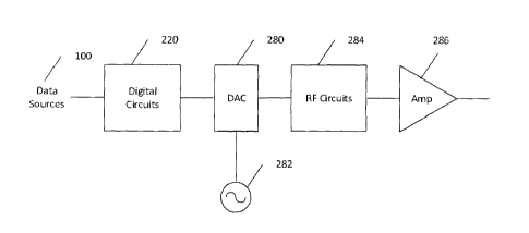
The basic configuration of the invention is shown in Figure 4. Although the
figures show
three paths, this invention is not limited to three paths and is scalable up
to many paths.
Multiple data sources, item 100, are fed to the digital circuits, where the
signals are
generated. The output of item 220 is a combined signal consisting of multiple
carriers
represented in a digital fashion. The output of the digital circuits is
applied to a DAC,
item 280, which is clocked by a signal generated by item 282, an oscillator.
The output
of item 280 is filtered by the RF circuits, item 284, which is then amplified
by item 286.
The digital circuits item 220 in Figure 4 is shown in more detail in Figure 5.
The digital circuits of item 220 can be implemented in a variety of ways,
including, but
not limited to, discrete logic, FPGA and ASICs.
Figure 5 shows details of the digital circuits of the invention. Data sources,
items 100,
102 and 104, feed modulators items 220, 222 and 224. The modulators perform:
grooming of the input signals, forward error correction, modulation and pulse
shaping
and amplitude control. Timing control item 226 controls the synchronization of
the
modulator. The output of the modulators is a multiple of their symbol rates.
Up-
samplers 230, 232 and 234, up-sample the output of the modulators to a sample
rate that
is common to all paths. This sample rate is chosen to be sufficient to allow
the
representation of all the required carriers in the required uplink bandwidth.
The up-
samplers increase the sample rate by a rational fraction. The up-samplers may
have
different rational fractions, allowing different symbol rates for each
channel.
CA 02883149 2015-02-25
Page 5
The output of the up-samplers, 230, 232 and 234 are at a common sampling rate
and are
placed relative to each other in frequency using mixers 240, 242 and 244 as
well as
numerically controlled oscillators (COs) 246, 248 and 250.
The outputs of each mixer, items 240, 242 and 244 are summed by an adder, item
252.
The output of the adder is up-sampled by item 260 to the DAC rate. The signal
is shifted
to its final output frequency by mixer 262 and NCO 264.
The signal is then applied to the DAC item 270.
In another embodiment of the invention items 230, 232,234, 240, 242, 244, 246,
248,
250, 252 are replaced by an FFT based channelizer.