Note: Descriptions are shown in the official language in which they were submitted.
CA 02884318 2015-03-06
DESCRIPTION
OPTICAL MULTIPLEXER/DEMULTIPLEXER
Technical Field
[0001]
The present invention relates to an optical
multiplexer/demultiplexer that functions as an optical filter
for a miniaturized optical transceiver adapted to make optical
communication. More specifically, the present invention
relates to an optical multiplexer/demultiplexer that is used
for an optical communication device necessary for connection
in a data center or between data centers.
Background Art
[0002]
With the progress of the Internet, in particular, because of
the expectation for progress in cloud computing, an increase
in capability of Ethernet-based communication is an urgent
challenge. As the next-generation high-speed 40G/100G
Ethernet (registered trademark) standard, IEEE 802.3ba (NPL 1)
was released in 2010, and discussions have been made. In
particular, the range of several tens m to several tens km in
transmission distance corresponds to a distance necessary for
connection in a data center or between data centers, and is
focused on because of large potential demand. In this standard,
- 1 -
CA 02884318 2015-03-06
in the range exceeding several tens m, the use of optical
communication is recommended because the attenuation of an
electric signal is large, and also in consideration of economic
efficiency, a multi-lane transmission system capable of
avoiding the heavy use of high-speed LSIs (Large Scale
Integration) is recommended. In particular, for a
transmission distance of several hundreds m or more, a
wavelength division multiplexing system using four wavelengths
in the wavelength arrangement such as LAN-WDM (Local Area
Network Wavelength Division Multiplexing) or CWDM (Coarse
Wavelength Division Multiplexing) in the 1.3 m band is
recommended.
[0003]
Devices responsible for realizing such transmission systems
closest to physical media are optical transceivers. In general,
an optical transceiver is configured to include: a connector
part that inputs/outputs optical and electrical signals; a TOSA
(Transmitter Optical Sub-Assembly) and ROSA (Receiver Optical
Sub-Assembly) that perform photoelectric conversion; an
electronic circuit that controls and monitors respective parts;
and an electronic circuit that performs signal conversion as
necessary. Further, the ROSA used for such transmission
systems is assembled with: an optical filter that demultiplexes
a multi-lane signal including four waves in the 1.3 m band;
four PDs (Photo Diodes); a TIA (Trans-Impedance Amplifier)
close to the PDs; and the like. For example, there has been
reported a ROSA that is prepared using an optical module
- 2 -
CA 02884318 2015-03-06
assembled with four small TFFs (Thin Film Filters) and a total
reflection mirror as a 4-ch optical demultiplexing filter (see
NPL 2). The ROSA reported in this literature realizes an
extremely small module size as a result of using the small TFF
chips and advanced packaging technology. However, the optical
module prepared using the plurality of TFFs becomes more
difficult to manufacture with increasing the number of channels
and reducing the size, and a reduction in size and a reduction
in cost cannot be easily achieved at the same time.
[0004]
On the other hand, an arrayed waveguide grating (AWG) optical
filter prepared with a silica-based PLC (Planar Lightwave
Circuit), which is a multi-channel optical filter, is widely
used for telecommunication transmission equipment because of
the excellence not only in wavelength demultiplexing
characteristics but in mass productivity and reliability.
Further, the AWG optical filter is characterized by excellent
economic efficiency and mass productivity because in particular,
in the case where the number of channels is large or a reduction
in size is required, as compares with the optical filter having
arranged TFFs, the number of manufacturing steps is small, and
the required tolerance of mechanical precision (TFF arrangement
precision and waveguide exposure precision) is large.
[0005]
However, the AWG had a problem once. In the initial stage of
AWG development, there was a problem that designing an AWG
having a channel spacing of several 10 nm or more caused an
- 3 -
CA 02884318 2015-03-06
increase in chip size. However, such a restriction has been
significantly relaxed by devising an arrayed waveguide
arrangement, and therefore today, even an AWG having a channel
spacing of 100 nm or more can be easily realized (see PTLs 1
and 2) .
[0006]
Regarding an AWG design method, a first conventional example
is described first using Fig. 1. Fig. 1 illustrates the outline
of a conventional arrayed waveguide grating optical filter. As
illustrated in Fig. 1, the arrayed waveguide grating optical
filter is configured to include slab waveguides 1 and 2, arrayed
waveguide group 3, input waveguide 4, and output waveguides 5.
Note that to appropriately operate the arrayed waveguide
grating optical filter, it is necessary that connecting points
between the waveguide group, which connects the slab waveguides
1 and 2 to each other, and the slab waveguides 1 and 2 are present
on extended lines of straight lines radially drawn from focal
points of the slab waveguides 1 and 2 on the input and output
waveguide sides, and between mutually adjacent ones of all
waveguides, the length is different by a certain amount (do) ,
and monotonically increases or decreases.
[0007]
In the arrayed waveguide grating filter illustrated in Fig. 1,
the arrayed waveguide group 3 is configured by sequentially
connecting respective waveguides, i.e., linear waveguides 3a,
arcuate waveguides 3c, and linear waveguides 3b, respectively.
Note that in the first conventional example, protruding
- 4 -
CA 02884318 2015-03-06
directions of arcs of the arcuate waveguides 3c are only one
direction, i.e., in the case of Fig. 1, an upward direction,
and therefore relative to lower waveguides of the arrayed
waveguide group 3, upper waveguides are longer. However, by
appropriately select lengths of the linear waveguides 3a and
3b and radii of the arcuate waveguides 3c, the array waveguide
group 3 can be arranged such that between any adjacent ones of
all the waveguides, the length is different by the certain
amount (c10)=
[0008]
On the other hand, the difference (do) in length between any
adjacent waveguides of the array waveguide group 3 has a
relationship given by the following expression (1) with
respective parameters (ko: center wavelength, ng: group
refractive index, and FSR: free spectral range) of the arrayed
waveguide grating optical filter. Note that in the following,
do is referred to as a waveguide length difference, and do x
nõ which is do multiplied by an effective refractive index ne,
is referred to as an optical path length difference.
[0009]
Wavelength interval x Maximum number of channels < ko2 / (do x
fl g) = FSR (1)
[0010]
In the case where a required wavelength interval is large, or
a large number of channels are required, it is necessary to set
the waveguide length difference do smaller; however, in the case
where the waveguide length difference do is extremely small,
- 5 -
CA 02884318 2015-03-06
in the arrayed waveguide group 3, an upper waveguide and a lower
waveguide come into contact with or intersect with each other
to make it difficult to appropriately operate the arrayed
waveguide grating optical filter. That is, according to the
first conventional technique described above, from geometrical
constraints, a settable waveguide length difference has a lower
limit, and therefore the design method according to the first
conventional example makes it geometrically impossible to set
the optical path length difference extremely short, or even if
the setting is possible, may anomalously increase the size of
a circuit.
[0011]
In the case of attempting to realize such a device as a waveguide
type, the size of a usable substrate material has a certain limit,
and accordingly in the case where the size of a circuit exceeds
the certain limit, manufacturing such a device is substantially
impossible. Therefore, it is difficult for a wide FSR arrayed
waveguide grating requiring setting an optical path length
difference extremely short, i.e., an arrayed waveguide grating
having a large wavelength interval at which
multiplexing/demultiplexing is performed or an arrayed
waveguide grating having a number of channels to employ such
a configuration.
[0012]
Next, a second conventional example is described using Fig. 2.
Note that PTL 1 discloses an arrayed waveguide grating filter
configured as an S-shaped optical waveguide according to the
- 6 -
CA 02884318 2015-03-06
second conventional example. Fig. 2 illustrates the outline
of the arrayed waveguide grating optical filter according to
the second embodiment . In Fig. 2, the arrayed waveguide grating
optical filter is configured to include slab waveguides 1 and
2, arrayed waveguide group 3, and a sectorial arcuate waveguide
group 6.
[0013]
As illustrated in Fig. 2, the slab waveguides 1 and 2 are
connected to each other through the S-shaped arrayed waveguide
group 3, and an overall circuit configuration is substantially
point symmetric. In the S-shaped optical waveguide, left
arcuate waveguides 3c and right arcuate waveguides 3d are
opposite in arc direction. Accordingly, in the case of directly
connecting the arcuate waveguides 3c and corresponding ones of
the arcuate waveguides 3d with the arcuate waveguide group 6
being omitted, respective waveguide lengths can be designed to
be substantially the same. That is, the S-shaped optical
waveguide is configured to once cancel out a waveguide length
difference necessary in geometrical arrangement at an
inflection point to zero.
[0014]
In the conventional example illustrated in Fig. 2, an optical
path length difference necessary for a filtering operation is
given by the sectorial arcuate waveguide group 6 inserted at
the inflection point of the S-shaped optical waveguide. The
sectorial arcuate waveguide group 6 is configured to include
arcuate waveguides among which a center point is the same, a
- 7 -
CA 02884318 2015-03-06
spread angle is the same, a spacing is the same, and a radius
increases by a certain amount. The optical path length
difference of this circuit is determined by a waveguide length
difference between any adjacent ones of the waveguides of the
sectorial arcuate waveguide group 6 (a difference in radius x
the spread angle) , and therefore even in the case of a wide FSR,
i.e. , even in the case where the optical path length difference
is extremely short, a desired circuit can be designed.
[0015]
On the other hand, the configuration as illustrated in Fig. 2
gives rise to a problem that the waveguide is point
symmetrically arranged on the basis of the S-shaped structure,
and therefore the length L of the circuit is large. As a result,
there is a problem that the size of the circuit exceeds the size
of an effective substrate, or even in the case where the circuit
can be arranged on the substrate, the number of circuits
arrangeable on one substrate is small.
[0016]
Next, a third conventional example is described using Fig. 3.
Fig. 3 illustrates the outline of an arrayed waveguide grating
optical filter according to the third conventional example.
The third conventional example is the arrayed waveguide grating
filter that is configured as a substantially line-symmetric
waveguide group (see Patent Literature 2) . As illustrated in
Fig. 3, the arrayed waveguide grating optical filter includes
slab waveguides 1 and 2, arrayed waveguide group 3, input
waveguide 4, output waveguides 5, and sectorial arcuate
- 8 -
CA 02884318 2015-03-06
waveguide group 6. In particular, the left side part of the
arrayed waveguide group 3 is configured as an arrayed waveguide
group 3g configured by sequentially connecting respective
waveguides, i.e., linear waveguides 3a, corresponding ones of
arcuate waveguides 3c, and corresponding ones of linear
waveguides 3e, and the right side part of the arrayed waveguide
group 3 is configured as an arrayed waveguide group 3h
configured by sequentially connecting respective waveguides,
i.e., linear waveguides 3f, corresponding ones of arcuate
waveguides 3d, and corresponding ones of linear waveguides 3b.
[0017]
In the arrayed waveguide group 3g and arrayed waveguide group
3h, a difference in length between upper and lower ones of
adjacent waveguides can be designed to be constant by, in the
same manner as the design method in the first conventional
example described using Fig. 1, appropriately selecting the
length of each of the linear waveguides and the radius of each
of the arcuate waveguides. However, protruding directions of
arcs of the arcuate waveguides 3c and arcuate waveguides 3d are
all upward, and therefore relative to a lower waveguide, an
upper waveguide is inevitably long. That is, only the arrayed
waveguide group 3g and arrayed waveguide group 3h of which the
protruding directions of the arcs are the same cannot make a
waveguide length difference zero.
[0018]
However, in Fig. 3, protruding directions of arcs of sectorial
arcuate waveguides 6 are opposite directions to those of the
- 9 -
CA 02884318 2015-03-06
arcuate waveguides 3c and arcuate waveguides 3d, and therefore
by appropriately selecting a spread angle and an arcuate radius
of the sectorial waveguide group 6 configured to include arcuate
waveguides among which a center point is the same, a spread angle
is the same, a spacing is constant, and a radius increases by
a certain amount, the waveguide length difference can be
configured to be once cancelled out to zero. After that, by
increasing or decreasing the spread angle of the sectorial
waveguides by a necessary amount, the waveguide length
difference of the arrayed waveguide group 3 can be easily set
to a value required by a wide FSR AWG. In the case of designing
an AWG by the design method according to the third example
described using Fig. 3, as compared with the design method
according to the second conventional example described using
Fig. 2, the degree of freedom of combination of arcuate
waveguides is different, and therefore an AWG having a smaller
circuit size may be designable.
Citation List
Patent Literature
[0019]
PTL 1: Japanese Patent No. 2693354
PTL 2: Japanese Patent No. 3222810
Non Patent Literature
[0020]
NPL 1: IEEE Std 802.3ba-
2010
http: //www.ieee802.org/3/ba/
- 10 -
CA 02884318 2015-03-06
NPL 2: K. Mochizuki, et al., "Built-in Optics for 4ch-WDM
ROSA in 100Gbps Ethernet", OECC2010
NPL 3: CFP Multi-Source
Agreement
http://www.cfp-msa.org/
NPL 4: S. Kamei, et al., "Low-loss and flat/wide-passband
CWDM demultiplexer using silica-based AWG with multi-mode
output waveguide", TuI2 OFC 2004
Summary of Invention
Technical Problem
[0021]
However, in addition to the IEEE recommendation, the industry
standard called MSA (Multi Source Agreement) regulates the size,
pin arrangement, and the like for optical transceivers, and for
optical transceivers for 40G/100G Ethernet, miniaturization
and power saving are strongly required (NPL 3) . In particular,
the outer size of modules discussed as CFP4 is approximately
9.5 x 21.7 x 88mm, which is extremely small (CFP: an abbreviation
of Form-factor Pluggable. "C" represents one hundred (100) in
Roman numerals.). In addition, inside a module of this size,
a ROSA and a TOSA, and an electronic circuit and the like
necessary for the transceiver should be arranged in parallel
and in series, respectively, and therefore a space allowed for
a single body of ROSA, and in addition a space allowed for an
optical filter incorporated in the ROSA are extremely small.
[0022]
- 11 -
CA 02884318 2015-03-06
Designing an AWG that performs multiplexing/demultiplexing in
a wavelength range corresponding to a large channel spacing such
as in LAN-WDM or CWDM recommended by IEEE has become possible
by the use of a sectorial arcuate waveguide group; however,
there is a challenge that a preparable AWG is elongated in
circuit form, and to contain the AWG in a module such as CFP4,
the circuit form should be shortened to further reduce the AWG
itself.
[0023]
The circuit size of the AWG main body can be reduced to some
extent by increasing a refractive index difference (A) of the
waveguide and decreasing a minimum bending radius; however, the
size of an output fan-out part adapted to be coupled to
individual PDs is also strongly dependent on a PD interval (or
a terminal interval of TIAs connected to the PDs), and therefore
there is a problem that sufficient miniaturization cannot be
performed only by increasing A.
[0024]
Further, specifications recommended by IEEE include not only
the optical wavelength channel spacing but also a wavelength
bandwidth of each channel. For this reason, it is necessary
to ensure a transmission wavelength bandwidth for an optical
filter. It is reported that configuring an output waveguide
as a multimode waveguide expands the transmission wavelength
bandwidth (NPT 4); however, as compared with a singlemode
waveguide, a multimode waveguide is large in minimum bending
radius. For this reason, the AWG by any of the design methods
- 12 -
CA 02884318 2015-03-06
according to the conventional examples has a problem that the
size of an output fan-out part (spread-out part) takes a large
space in layout.
[0025]
On the other hand, optical transceivers for Ethernet are
supposed to be often used for connection in a data center and
between data centers, and therefore compete with inexpensive
electrical signal transceivers, so that the optical
transceivers for Ethernet require a considerable reduction in
cost as compared with optical transceivers for
telecommunications.
[0026]
An optical filter used for a ROSA should be, on the input side,
optically coupled to a connector of an optical cable through
an optical component called a receptacle, and on the output side,
optically connected to four PDs through optical lenses. When
assembling the ROSA, these components should be precisely
aligned and fixed so as to prevent mutual misalignment.
[0027]
The simplest method as an alignment method is one that makes
light having an actually used signal light wavelength enter from
the above-described optical cable, and pass sequentially
through the optical filter, optical lenses, and PDs, and then
while monitoring electrical outputs from the PDs, collectively
performs multi-body alignment of all the components. However,
this method requires a very complicated multi-body aligner, and
therefore has a problem of extremely high cost.
- 13 -
CA 02884318 2015-03-06
[0028]
Also, for a PD, optical filter, and optical fiber, different
types of materials having very different refractive indices
must be inevitably selected, and accordingly reflection at
boundaries between the materials occurs. Further, in the case
of using a lens system in order to increase coupling efficiency
of each optical coupling, an air layer is added for each lens
surface, and consequently reflection occurs many more times.
To improve received S/N, typically, an antireflective film is
provided for a telecommunication purpose; however, for an
Ethernet purpose, a there is a challenge of avoiding an increase
in cost along with the increase in processing step.
[0029]
The present invention is made in consideration of the
above-described conventional problems, and intends to provide
a multiplexer/demultiplexer that can constitute a miniaturized,
low-cost ROSA module necessary to realize high-speed Ethernet
transceivers, and functions as an extremely small AWG optical
filter. Further, another object is to suppress an increase in
manufacturing cost of the ROSA module caused by a circuit added
to the AWG optical filer, and the shape of a chip.
Solution to Problem
[0030]
In order to solve the above problems, an invention described
in an embodiment is an optical multiplexer/demultiplexer
including: at least one input waveguide that has an input part
at one end; a first slab waveguide of which one end is connected
- 14 -
CA 02884318 2016-10-24
95546-28T
to the other end of the input waveguide; an arrayed waveguide
group of which one end is connected to the other end of the first
slab waveguide, the arrayed waveguide group having multiple
waveguides; a second slab waveguide of which one end is connected
to the other end of the arrayed waveguide group; and at least
one output waveguide of which one ends are connected to the other
end of the second slab waveguide and the other ends respectively
have output parts, wherein each of the waveguides of the arrayed
waveguide group has: a first bent part of which a waveguide
extending direction changes 180 degrees or more; and a second
bent part of which a waveguide extending direction changes 180
degrees or more in a direction opposite to a direction of the
change of the first bent part.
[0030a]
In one aspect, there is provided an optical
multiplexer/demultiplexer comprising: at least one input
waveguide that has an input part at one end; a first slab
waveguide of which one end is connected to the other end of the
input waveguide; an arrayed waveguide group of which one end
is connected to the other end of the first slab waveguide, the
arrayed waveguide group having a plurality of waveguides;
a second slab waveguide of which one end is connected to the
other end of the arrayed waveguide group; and at least one output
waveguide of which one ends are connected to the other end of
the second slab waveguide and the other ends respectively have
output parts, wherein each of the waveguides of the arrayed
waveguide group is configured as an S-shaped waveguide having
a first curved part and a second curved part: one end of the
- 15 -
CA 02884318 2016-10-24
95546-28T
first curved part is connected to the first slab waveguide, a
waveguide extending direction of the first curved part changes
180 degrees or more, one end of the second curved part is
connected to the other end of the first curved part, the other
end of the second curved part is connected to the second slab
waveguide, and a waveguide extending direction of the second
curved part changes 180 degrees or more in a direction opposite
to the direction of the change of the first curved part.
Brief Description of Drawings
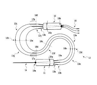
[0031]
[Fig. 1] Fig. 1 is a schematic diagram of an arrayed
waveguide grating optical filter according to a first
conventional example;
[Fig. 2] Fig. 2 is a schematic diagram of an arrayed
waveguide grating optical filter according to a second
conventional example;
[Fig. 3] Fig. 3 is a schematic diagram of an arrayed
waveguide grating optical filter according to a third
conventional example;
[Fig. 4] Fig. 4 is a schematic diagram of an arrayed
waveguide grating optical filter according to a first example;
[Fig. 5] Fig. 5 is a waveguide arrangement diagram of an
arrayed waveguide grating optical filter for CWDM signal
four-channel demultiplexing designed in the first example;
[Fig. 6] Fig. 6 is a waveguide arrangement diagram of an
arrayed waveguide grating optical filter for CWDM signal
- 16 -
CA 02884318 2015-03-06
four-channel demultiplexing designed in the second
conventional example;
[Fig. 7] Fig. 7 is a waveguide arrangement diagram of an
arrayed waveguide grating optical filter for CWDM signal
four-channel demultiplexing designed in the third conventional
example;
[Fig. 8] Fig. 8 is a waveguide arrangement diagram of an
aligning waveguide-equipped arrayed waveguide grating optical
filter for LAN-WDM signal demultiplexing designed in a second
example;
[Fig. 9A] Fig. =9A is a diagram illustrating a first step
of work to aligning an input side member (receptacle) and output
side members (PD arrays and the like) with the aligning
waveguide-equipped arrayed waveguide grating optical filter
designed in the second example;
[Fig. 9B] Fig. 9B is a diagram illustrating a second step
of the work to aligning the input side member (receptacle) and
the output side members (PD arrays and the like) with the
aligning waveguide-equipped arrayed waveguide grating optical
filter designed in the second example;
[Fig. 9C] Fig. 9C is a diagram illustrating a third step
of the work to aligning the input side member (receptacle) and
the output side members (PD arrays and the like) with the
aligning waveguide-equipped arrayed waveguide grating optical
filter designed in the second example;
[Fig. 9D] Fig. 9D is a diagram illustrating a fourth step
of the work to aligning the input side member (receptacle) and
- 17 -
CA 02884318 2015-03-06
the output side members (PD arrays and the like) with the
aligning waveguide-equipped arrayed waveguide grating optical
filter designed in the second example; and
[Fig. 10] Fig. 10 is a graph illustrating the wavelength
dependency of conversion efficiency of a ROSA module prepared
in the second example.
Description of Embodiments
[0032]
Embodiments of the present invention will hereinafter be
described in detail.
[0033]
An optical multiplexer/demultiplexer of the present invention
is an arrayed waveguide grating optical
multiplexer/demultiplexer including: at least one input
waveguide; a first slab waveguide that is connected to the input
waveguide; an arrayed waveguide group that is connected to the
first slab waveguide and includes a plurality of
parallel-arranged waveguides; a second slab waveguide that is
connected to the arrayed waveguide group; and at least one
output waveguide that are connected to the second slab waveguide,
and configured such that the respective waveguides of the
arrayed waveguide group connected to the first slab change
extending directions of the respective waveguides 180 degrees
or more, then change the extending directions of the waveguides
180 degrees or more in an opposite direction, and are then
connected to the second slab. Here, it can be said that the
- 18 -
CA 02884318 2015-03-06
"extending directions of the waveguides" are the same as optical
axis directions of lights guided in the waveguides,
respectively. Also, it can be said that the arrayed waveguide
group has the following configurations (1) to (3) .
[0034]
(1) Each of the waveguides of the arrayed waveguide group
includes a first part and a second part, in which the first part
is from an exit end of the input slab waveguide (first slab
waveguide) to a connecting point of the second part, of which
an optical path bends 180 degrees or more from the exit end in
a first direction, and the second part is from a connecting point
of the first part to an entrance end of the output slab waveguide
(second slab waveguide) , of which an optical path bends 180
degrees or more from the connecting point in a second direction
opposite to the first direction. Note that in this description,
a "bent" optical path refers to an optical path of which the
entire part may not necessarily be bent, and also includes a
configuration having a part where a curvature of the optical
path is zero.
[0035]
(2) Each of the waveguides of the arrayed waveguide group
includes a first part and a second part, in which the first part
is from the exit end of the input slab waveguide to the connecting
point of the second part, and includes an arcuate waveguide bent
180 degrees or more in the first direction, and the second part
is from the connecting point of the first part to the entrance
end of the output slab waveguide, and includes an arcuate
- 19 -
CA 02884318 2015-03-06
waveguide bent 180 degrees or more in the second direction
opposite to the first direction. Note that in this description,
an "arcuate waveguide" refers to a wave guide of which the entire
part may not necessarily be bent, and also includes a
configuration having a part where a curvature of the waveguide
is zero.
[0036]
(3) Each of the waveguides of the arrayed waveguide group
includes a first arcuate waveguide and a second arcuate
waveguide, in which the first arcuate waveguide is bent 180
degrees or more in the first direction from the exit end of the
input slab waveguide and is connected to the second arcuate
waveguide, and the second arcuate waveguide is bent 180 degrees
or more in the second direction opposite to the first direction
from a connecting point of the first arcuate waveguide, and is
connected to the entrance end of the output slab waveguide.
[0037]
Each of the arrayed waveguides connected to the first slab
waveguide once changes an extending direction thereof 180
degrees or more, further change the extending direction 180
degrees or more in an opposite direction, and is then connected
to the second slab. With this configuration, even a wide FSR
AWG can be decreased in area of a main body thereof without being
formed in an elongated shape.
[0038]
Preferably, a connecting point between the input waveguide and
the first slab waveguide and a connecting point between the
- 20 -
CA 02884318 2015-03-06
second slab waveguide and the output waveguides are arranged
on the inside between the rightmost end and leftmost end of an
area where the arrayed waveguide group including the plurality
of parallel-arranged waveguides is arranged, and the connecting
point between the input waveguide and the first slab waveguide
and the connecting point between the second slab waveguide and
the output waveguides are arranged on the inside between the
uppermost end and lowermost end of the area where the arrayed
waveguide group including the plurality of parallel-arranged
waveguides is arranged.
[0039]
By arranging the two slab waveguides not at both ends but on
the inner side in layout, input and output fan-out parts of the
AWG can be efficiently arranged, and a footprint of the AWG
including the output fan-out part can be decreased.
[0040]
Also, preferably, there is an aligning input waveguide reaching
a third side that is different from a first side of optical
multiplexer/ de multiplexer reached by the input waveguide, and
different from a second side reached by at least one of the output
waveguides; the aligning input waveguide is connected to the
first slab waveguide; and one ends of two of the plurality of
output waveguides, which are not connected to the second slab
waveguide, are mutually connected to thereby form the two output
waveguides into a loop shape.
[0041]
- 21 -
CA 02884318 2015-03-06
One end of the aligning input waveguide is connected to the one
slab waveguide, and the looped waveguide is connected to the
other slab waveguide. This configuration makes it possible to
make aligning lights exit from both of input and output
waveguides of the AWG by selecting wavelengths of the lights
inputting to the aligning input waveguide.
[0042]
Further, preferably, of the input waveguide, output waveguides,
and aligning input waveguide, at least one waveguide reach at
least one chip side while having a tilt of eight degrees or more
from a normal direction to the chip sides.
[0043]
Only by dicing the chip along a side reached by each of the input
and output waveguides or aligning input waveguide, a return loss
can be suppressed without performing oblique polishing or an
antireflection film coating step. As a result, a polishing step
can be omitted, and correspondingly a cost can be reduced.
[0044]
(First example)
Fig. 4 illustrates the outline of an arrayed waveguide grating
optical filter according to this example. As illustrated in
Fig. 4, the arrayed waveguide grating optical filter according
to this example includes a first slab waveguide 11, second slab
waveguide 12, arrayed waveguide group 13, input waveguide 14,
and output waveguides 15.
[0045]
- 22 -
CA 02884318 2015-03-06
The arrayed waveguide group 13 is an arrayed waveguide group
including S-shaped waveguides respectively configured by
connecting linear waveguide 13a, arcuate waveguides 13b,
arcuate waveguides 13c, linear waveguides 13d, arcuate
waveguides 13e, arcuate waveguides 13f, first waveguide length
difference adjusting linear waveguides 17a, arcuate waveguides
13g, linear waveguides 13h, arcuate waveguides 13i, second
waveguide length difference adjusting linear waveguides 17b,
arcuate waveguides 13j, and linear waveguides 13k in series,
and the total length of each of the S-shaped waveguides
monotonously increases or decreases by a constant value between
any adjacent ones of the waveguides.
[0046]
Note that the length of each of the waveguides, i.e., from the
linear waveguides 13a to the linear waveguides 13k, and the
length of each of the waveguides, i.e., the first waveguide
length difference adjusting linear waveguides 17a and the
second waveguide length difference adjusting waveguides 17b may
be respectively zero.
[0047]
The respective S-shaped waveguides constituting the arrayed
waveguide group 13 orthogonally intersect with a first
reference line 18a via the linear waveguides 13a and arcuate
waveguides 13b from the first slab waveguide 11, orthogonally
intersect with a second reference line 18b via the arcuate
waveguides 13c and linear waveguides 13d, orthogonally
intersect with a third reference line 18c via the arcuate
- 23 -
CA 02884318 2015-03-06
waveguides 13e, orthogonally intersect with a fourth reference
line 18d via the arcuate waveguides 13f, orthogonally intersect
with a fifth reference line 18e via the first waveguide length
difference adjusting linear waveguides 17a and arcuate
waveguides 13g, orthogonally intersect with the sixth reference
line 18f via the linear waveguides 13h, arcuate waveguides 13i,
and second waveguide length difference adjusting linear
waveguides 17b, and is coupled to the second slab waveguide 12
via the arcuate waveguides 13j and linear waveguides 13k.
[0048]
Among the respective S-shaped waveguides constituting the
arrayed waveguide group 13, when setting a propagation
direction of optical signals to a direction from the first slab
waveguide 11 toward the second slab waveguide 12, the arcuate
waveguides 13c and the arcuate waveguides 13e are concaved
leftward with respect to the propagation direction, and the
arcuate waveguides 13f, arcuate waveguides 13g, and arcuate
waveguide 13i are concaved rightward with respect to the
propagation direction. The total of spread angles of the
arcuate waveguides 13c and arcuate waveguides 132 are designed
to have the same value as the total of spread angles of the
arcuate waveguides 13f, arcuate waveguides 13g, and arcuate
waveguides 13i. For this reason, except for the first waveguide
length difference adjusting linear waveguides 17a and the
second waveguide length difference adjusting linear waveguides
17b, the lengths of the respective S-shaped waveguides are
substantially the same.
- 24 -
CA 02884318 2015-03-06
[0049]
Strictly, the sum of the lengths of each of the linear waveguides
13a and a corresponding one of the arcuate waveguides 13b after
the first slab waveguide 11 and before orthogonally
intersecting with the first reference line 18a and the lengths
of corresponding ones of the arcuate waveguides 13j and linear
waveguides 13k after orthogonally intersecting the sixth
reference line 18f and before being coupled to the second slab
waveguide 12 is different for each of the S-shaped waveguides.
In addition, the lengths of each of the linear waveguides 13d
and a corresponding one of the linear waveguides 13h are also
different for each of the S-shaped waveguides. The differences
in length are caused by the fact that extended lines of the linear
waveguides 13a intersect with one another at a first reference
point 19a, and extended lines of the linear waveguides 13k
intersect with each other at a second reference point 19b. A
spread angle 20a of the linear waveguides 13a around the first
reference point 19a, and a spread angle 20b of the linear
waveguides 13k around the second reference point 19b give
substantially the same values as numerical apertures of the
input waveguide 14 and the output waveguides 15 through design.
As a result, a difference in total length between any adjacent
ones of the S-shaped waveguides falls below approximately a few
[im. However, the difference in total length between any
adjacent ones of the S-shaped waveguides has a finite value,
but the difference in the total length each of the S-shaped
waveguides can be designed to be strictly zero by adjusting the
- 25 -
CA 02884318 2015-03-06
lengths of the first waveguide length difference adjusting
linear waveguides 17a and the lengths of the second waveguide
length difference adjusting linear waveguides 17b.
[0050]
The arrayed waveguide group 13 has a first bend part formed of
the waveguides from the first reference line 18a to the third
reference line 18c, and a second bent part formed of the
waveguides from the third reference line 18c to the sixth
reference line 18f. The first bent part is a part where the
waveguides constituting the arrayed waveguide group 13 is bent
180 degrees or more. The second bend part is a part where the
waveguides constituting the arrayed waveguide group 13 is bent
180 degrees or more in a direction opposite to a bending
direction of the first bent part. Accordingly, the optical axis
directions of the lights guided in the arrayed waveguide group
13 change by 180 degrees or more from the first reference line
18a to the third reference line 18c, and change by 180 degrees
or more in the direction opposite to the bending direction of
the first bent part from the third reference line 18c to the
sixth reference line 18f.
[0051]
To operate the arrayed waveguide grating optical filter
illustrated in Fig. 4 as a wavelength multiplexer/demultiplexer
filter, it is only necessary to first calculate a waveguide
length difference do from a desired FSR using the
above-described expression (1) (the numerical expression is
given below again), and design the lengths of the first
- 26 -
CA 02884318 2015-03-06
waveguide length difference adjusting linear waveguides 17a and
the lengths of the second waveguide length difference adjusting
linear waveguides 17b so as to make the waveguide length
difference do equal to the difference in total length between
any adjacent ones of the S-shaped waveguides.
[0052]
Wavelength interval x Maximum number of channels < X02 / (do x
ng) = FSR (1)
[0053]
In the above expression (1), X0: center wavelength, ng: group
refractive index, and FSR: free spectral range.
[0054]
Fig. 5 is a waveguide arrangement diagram of an arrayed
waveguide grating optical filter for CWDM signal 4-channel
demultiplexing actually designed by the above-described design
method. A waveguide used was an embedded waveguide using silica
glass doped with germanium, in which a refractive index
difference was adjusted to 2 %, and the core height and core
width of a reference waveguide were respectively adjusted to
4 m and 4 m. In this reference waveguide, a minimum bending
radius in the 1300-nm band was 750 m as described above.
Wavelengths of demultiplexed optical signals were set to 1271
nm, 1291 nm, 1311 nm, and 1331 nm, and in order to reduce a
difference in transmission loss between channels, the FSR was
set to 3250 GHz. As a result, the waveguide length difference
provided between any adjacent S-shaped arrayed waveguides was
set to 6.498 m.
- 27 -
CA 02884318 2015-03-06
[0055]
In addition, to exhibit flatness in a transmission range in
multiplexing/demultiplexing characteristics, waveguide
widths of the input waveguide 14 and output waveguides 15 were
set to different values, respectively. Specifically, the
width of the input waveguide 14 connected to the first slab
waveguide 11 was set to 8.0 tm, and the width of the four output
waveguides 15 connected to the second slab waveguide 12 were
set to 15 In. In addition, since higher-order mode lights were
also propagated through the output waveguides 15 having a width
of 15 m, a minimum bending radius was set to 1200 m. Also,
a spacing between adjacent light receiving surfaces of an array
of four successive PDs prepared was 250 m, and therefore a
spacing between adjacent output waveguides was set to 250 m.
It was expected that the minimum bending radius and the output
waveguide spacing increased a fan-out part 22 of the output
waveguides, and therefore the connecting point between the
second slab waveguide 12 and the output waveguides 15 was
arranged on the inside between the rightmost end and leftmost
end of an area where the arrayed waveguide group 13 was arranged
and on the inside between the uppermost end and the lowermost
end of an area where the arrayed waveguide group 13 was arranged.
That is, the connecting point between the second slab waveguide
12 and the output waveguides 15 is arranged so as to make a
distance from a side of a chip where the waveguides are formed
(in Fig. 5, indicated by a rectangular frame surrounding the
waveguides) to the second slab waveguide 12 larger than a
- 28 -
CA 02884318 2015-03-06
distance from the side of the chip to the arrayed waveguide group
13.
[0056]
Also, as illustrated in Fig. 5, the connecting point between
the first slab waveguide 11 and the input waveguide 14 was
arranged on the inside between the rightmost end and leftmost
end of the area where the arrayed waveguide group 13 was arranged
and on the inside between the uppermost end and the lowermost
end of an area where the arrayed waveguide group 13 was arranged.
That is, the connecting point between the first slab waveguide
11 and the input waveguide 14 is arranged so as to make a distance
from a side of the chip where the waveguides are formed to the
slab waveguide 11 larger than a distance from the side of the
chip to the arrayed waveguide group 13. Note that the specific
arrangement of the arrayed waveguide group 13 was designed
according to the design method described using Fig. 4.
[0057]
Further, in order to suppress reflection at the chip ends of
the output waveguides, the output waveguides were designed so
as to reach the side of the chip on the output side while having
a tile of 8 degrees from a normal direction to the side of the
chip. In addition, the input waveguide may also be designed
so as to reach the side of the chip on the input side while having
a tilt of 8 degrees with respect to the side of the chip.
[0058]
As described, as a result of specifically designing the layout
of the arrayed waveguide grating optical
- 29 -
CA 02884318 2015-03-06
multiplexer/demultiplexer according to the design method of the
present invention, as illustrated in Fig. 5, the AWG was able
to be arranged within a small footprint, i.e., a chip size of
8.2 mm long by 4.9 mm wide.
{0059]
Further, the connecting point between the second slab waveguide
12 and the output waveguides 15 was arranged on the inside
between the rightmost end and leftmost end of the area where
the arrayed waveguide group 13 was arranged and on the inside
between the uppermost end and the lower most end of an area where
the arrayed waveguide group 13 was arranged, and therefore
positions of the output waveguides 15 at the chip end were able
to be arranged in the center of the chip as a secondary effect.
By being able to arrange the positions of the output waveguides
15 at the chip end in the center of the chip, the need for a
wasted space extending in the vertical direction when
assembling PDs, TIAs, and lead-out electrodes is eliminated,
and therefore there is the advantage of being able to eventually
decrease a ROSA module size.
[0060]
Fig. 6 illustrates a result of calculating the layout of an
arrayed waveguide grating optical multiplexer/demultiplexer
having the same wavelength arrangement and the same wavelength
structure according to the design method of the second
conventional example for comparison. An arrayed waveguide
group 13 of the arrayed waveguide grating optical
multiplexer/demultiplexer illustrated in Fig. 6 includes
- 30 -
CA 02884318 2015-03-06
parallel-arranged S-shaped optical waveguides, and as a whole,
has substantially point symmetric structure. The size of a
completed chip was 11.8 mm long by 3.9 mm wide. The chip width
of 3.9 mm is narrower than that of the arrayed waveguide grating
optical multiplexer/demultiplexer illustrated in Fig. 5.
However, in the case of adding a restriction that arranges the
positions of output waveguides 15 at the side of the chip in
the center, the chip width requires 6.4 mm. That is, the chip
width is made larger than that of the arrayed waveguide grating
optical multiplexer/demultiplexer according to the design
method of the present invention. Also, the chip length of 11.8
mm was 3.6 mm longer, i.e., approximately 44 % longer in ratio
than that of the arrayed waveguide grating optical
multiplexer/demultiplexer illustrated in Fig. 5 according to
the design method of the present invention.
[0061]
Further, Fig. 7 illustrates a result of calculating the layout
of an arrayed waveguide grating optical
multiplexer/demultiplexer having the same wavelength
arrangement and the same wavelength structure according to the
design method of the third conventional example for comparison.
An arrayed waveguide group 13 of the arrayed waveguide grating
optical multiplexer/demultiplexer illustrated in Fig. 7 has
substantially line symmetric structure as a whole. Between the
central part and both side parts of the arrayed waveguide group
13, protruding directions of an arc of an arcuate waveguide are
opposite to each other. The size of a completed chip was 14.3
- 31 -
CA 02884318 2015-03-06
mm long by 3.1 mm wide. Even in the case of adding the
restriction that arranges the positions of output waveguides
15 at the side of the chip in the center, the chip width was
able to be formed as narrowly as 4.1 mm. However, the chip
length of 14.3 mm was 6.1 mm longer, i.e., approximately 75 %
longer in ratio than that of the arrayed waveguide grating
optical multiplexer/demultiplexer illustrated in Fig. 5
according to the design method of the present invention.
[0062]
The arrayed waveguide grating optical
multiplexer/demultiplexer illustrated in Fig. 5 according to
the design method of the present invention, the arrayed
waveguide grating optical multiplexer/demultiplexer
illustrated in Fig. 6 according to the design method of the
second conventional example, and the arrayed waveguide grating
optical multiplexer/demultiplexer illustrated in Fig.7
according to the design method of the third conventional example
respectively have chip areas of approximately 40 mm square,
approximately 46 mm square, and approximately 44 mm square when
removing the restriction that arranges the positions of output
waveguides in the center of a chip. Accordingly, when
estimating a unit chip cost from a yield per wafer, it turned
out that by using the arrayed waveguide grating optical
multiplexer/demultiplexer according to the design method of the
present invention, the effect of reducing a unit chip cost by
approximately 15 % as compared with the optical
multiplexer/demultiplexer of the first conventional example,
- 32 -
CA 02884318 2015-03-06
and by approximately 10 % as compared with the optical
multiplexer/demultiplexer of the second conventional example
was obtained.
[0063]
In the arrayed waveguide grating optical
multiplexer/demultiplexer in this example, the waveguides of
the arrayed waveguide group change extending directions thereof
180 degree or more once, and then change the extending
directions thereof in an opposite direction. Further, the
first slab waveguide and the second slab waveguide are arranged
on the inside between the rightmost end and leftmost end of the
area where the arrayed waveguide group is arranged, and on the
inside between the uppermost end and the lowermost end of the
area where the arrayed waveguide group is arranged. As a result,
a small chip size is achieved.
[0064]
Further, in this example, the extending directions of the
waveguides are changed 180 degrees or more, and the
miniaturization is achieved with low loss. This is achieved
by using the waveguides that are resistant to a steep bend as
compared with a typical silica-based glass waveguide (a
refractive index difference of 1 % or less). In the case of
the typical silica-based glass waveguide, a minimum bending
radius with which the waveguide can be bent is 2 mm or more.
When bending the typical silica-based glass waveguide further
steeply, transmission light cannot fully bend, and is emitted
outside the waveguide as radiation light. For this reason, when
- 33 -
CA 02884318 2015-03-06
using the typical waveguide fora steep bend, a loss of an arrayed
waveguide multiplexer/demultiplexer becomes large.
However, when using a waveguide having a refractive index
difference of 2 % or more, a steeper bend with a minimum bending
radius of 750 mm or less (in the 1300 nm wavelength band) can
be achieved which is steeper than a bend of the typical
waveguide.
[0065]
In this example, by using the waveguides having the refractive
index difference of 2 % or more, a low loss arrayed waveguide
multiplexer/demultiplexer is realized with the miniaturized
configuration in which the extending directions of the
waveguides are changed 180 degrees or more.
[0066]
(Second example)
In this example, in order to make the arrayed waveguide grading
optical multiplexer/demultiplexer in the first example
function as an aligning waveguide-equipped arrayed waveguide
grating optical filter for LAN-WDM signal demultiplexing, the
arrayed waveguide grating optical multiplexer/demultiplexer
is configured such that wavelengths of optical signals to be
demultiplexed are different. Fig. 8 is a waveguide arrangement
diagram of the aligning waveguide-equipped arrayed waveguide
grating optical filter for LAN-WDM signal demultiplexing
designed in this example. Materials for waveguides and
waveguide parameters used are the same as those of the arrayed
waveguide grating optical multiplexer/demultiplexer
- 34 -
CA 02884318 2015-03-06
illustrated in FIG. 5; however, wavelengths of optical signals
to be demultiplexed are different. The wavelengths of the four
waves were set to 1295.56 nm, 1300.05 nm, 1304.58 nm, and 1309.14
nm, and in consideration of a difference in transmission loss
between channels, an FSR was set to 7830 GHz. As a result, a
waveguide length difference given between any adjacent S-shaped
arrayed waveguides was set to 25.79 [tm. Also, as in the arrayed
waveguide grating optical multiplexer/demultiplexer
illustrated in Fig. 5, in order to exhibit flatness in a
transmission range in
multiplexing/demultiplexing
characteristics, waveguide widths of an input waveguide 14 and
output waveguides 15 were set to different values, respectively.
Specifically, the width of the input waveguide 14 connected to
a first slab waveguide 11 was set to 8.0 [tm, and the width of
the four output waveguides 15 connected to a second slab
waveguide 12 was set to 15 pm.
[0067]
Further, a minimum bending radius of the output waveguides
having a width of 15 lam was set to 1200 [tm, and a spacing between
any adjacent ones of the output waveguides 15 at a chip side
was set to 250 i_tra. In order to efficiently arrange a fan-out
part 22 of the output waveguides 15, as in the arrayed waveguide
grating optical multiplexer/demultiplexer illustrated in Fig.
5, a connecting point between the first slab waveguide 11 and
the input waveguide 14 and a connecting point between the second
slab waveguide 12 and the output waveguides 15 were arranged
on the inside between the rightmost end and leftmost end of an
- 35 -
CA 02884318 2015-03-06
area where the arrayed waveguide group 13 was arranged, and on
the inside between the uppermost end and the lowermost end of
an area where the arrayed waveguide group 13 was arranged.
[0068]
The this example is configured to, on both sides of the output
waveguides 15 as the four multimode waveguides illustrated in
Fig.8, additionally arrange a set of (two) first aligning light
output waveguides 30 as single mode waveguides for aligning an
optical lens array, and a set of (two) second aligning light
output waveguides 31 as single mode waveguides for aligning a
PD array. Further, the left and right sides of the chip of the
arrayed waveguide grating optical multiplexer/demultiplexer
were respectively connected with optical components, and
therefore an aligning light input waveguide 32 was arranged on
the upper side of the chip. Note that the aligning light input
waveguide 32 is connected to the first slab waveguide 11
connected with the input waveguide 14 of the arrayed waveguide
grating optical multiplexer/demultiplexer. On the other hand,
the second slab waveguide 12 connected with the output
waveguides 15 of the arrayed waveguide grating optical
multiplexer/demultiplexer was connected with a looped
waveguide 33 so as to make it possible for an optical signal
inputted from the aligning light input waveguide 32 to turn back.
Further, beside the looped waveguide 33, a third aligning light
output waveguide 34 that gave an output to the lower side of
the chip was placed.
[0069]
- 36 -
CA 02884318 2015-03-06
Note that in order to make a return loss equal to or more than
40 dB, an angle formed between each of the output waveguides
15, set of (two) first aligning light output waveguides 30, and
set of (two) aligning light output waveguides 31, which were
placed on the right side of the chip, and the right side of the
chip was set to eight degrees. Also, an angle of the aligning
light input waveguide 32 with respect to the upper side of the
chip, and an angle of the third aligning light output waveguide
34 with respect to the lower side of the chip were set to 8 degrees.
The end surface of the left side of the chip was applied with
AR (Anti-Reflection) coating for suppressing a reflected amount
in the 1.3 band, and therefore an angle formed between the input
waveguide 14 and the left side of the chip was set to a right
angle.
[0070]
As a result of the above design, when inputting lights in the
1.3 fim band from the aligning light input waveguide 32 on the
upper side of the chip, light having a wavelength of 1324.2 nm
is outputted from the third aligning light output waveguide 34
on the lower side of the chip; lights having wavelengths of
1287.8 nm and 1308.0 nm are outputted from the set of first
aligning light output waveguides 30 for optical lens array
alignment, respectively; lights having wavelengths of 1285.6
nm and 1310.28 nm are outputted from the set of second aligning
light output waveguides 31 for PD array alignment,
respectively; and light having a wavelength of 1319.5 nm is
outputted to the input waveguide 14 of the arrayed waveguide
- 37 -
CA 02884318 2015-03-06
grating optical filter for aligning and placing a receptacle
member. The light is outputted to the input waveguide 14
through the following path. The light having a wavelength of
1319.5 nm among the lights entering the aligning light input
waveguide 32 travels through the first slab waveguide 11 and
second slab waveguide 12, then travels through the looped
waveguide 33, again enters the second slab waveguide 12, and
from the first slab waveguide 11, is outputted to the input
waveguide 14.
[0071]
Figs. 9A, 9B, 9C, and 9D are schematic diagrams illustrating
steps of assembling an optical lens array 36, a member for
receptacle 37, and a PD array-integrated member 38 to the chip
35 of the aligning waveguide-equipped arrayed waveguide grating
optical filter for LAN-WDM signal demultiplexing illustrated
in Fig. 8.
[0072]
First, a single-core optical fiber block 39 is temporarily fixed
to the aligning light input waveguide 32 on the chip upper side,
not on the left or right side of the optical filter chip 35 to
be assembled with the optical components, using the light having
a wavelength of 1324.2 nm (Fig. 9A). More specifically, the
exiting light from the third aligning light output waveguide
34 on the lower side of the optical filter chip 35 is received
using a large diameter PD 40 to perform two-body alignment of
the optical filter chip 35 and the single-core optical fiber
block 39, and then temporary fixation is performed. Note that
- 38 -
CA 02884318 2015-03-06
the temporary fixation is performed using a low adhesive
strength adhesive or adhesive condition so as to make it
possible to remove the single-core optical fiber block 39 after
the assembling steps. Also, the end surface of the single-core
optical fiber block 39 used here is polished at eight degrees,
and therefore optical coupling can be performed with a loss and
reflection at the chip upper side being suppressed small.
[0073]
Then, when inputting the lights respectively having wavelengths
of 1287.8 nm and 1308.0 nm to the aligning light input waveguide
32 on the chip upper side through the temporarily fixed
single-core optical fiber block 39, the lights are outputted
from the first aligning light output waveguides 30. The
outputted lights are used to align the optical lens array 36
with a two-body aligner, and after completion of the alignment,
the optical lens array 36 is fixed with an adhesive (Fig. 9B) .
[0074]
As a third step, when inputting the light having a wavelength
of 1319.5 nm to the aligning input waveguide 32 on the chip upper
side through the temporarily fixed single-core optical fiber
block 39, the light is outputted from the input waveguide 14
of the arrayed waveguide grating optical filter. The outputted
light is used to align the receptacle member 37 with the two-body
aligner, and after completion of the alignment, the member for
receptacle 37 is fixed with an adhesive (Fig. 9C) .
[0075]
- 39 -
CA 02884318 2015-03-06
As a fourth step, when inputting the lights respectively having
wavelengths of 1285.6 nm and 1310.28 nm to the aligning light
input waveguide 32 on the chip upper side through the
temporarily fixed single-core optical fiber block 39, the
lights are outputted from the second aligning light output
waveguides 31. The outputted lights are used to align the PD
array-integrated member 38 with the two-body aligner, and after
completion of the alignment, the PD array-integrated member 38
is fixed with an adhesive (Fig. 9D) .
[0076]
Finally, by applying torsional stress to remove the temporarily
fixed single-core optical fiber block 39 from the optical filter
chip 35, the assembling around the optical filter chip 35 is
ended.
[0077]
The important thing here is that the assembling of the
peripheral members to the arrayed waveguide grating optical
multiplexer/demultiplexer of the present invention described
using Figs. 9A, 9B, 9C, and 9D can be performed using only the
two-body aligner without using an expensive multi-body aligner
at all, which is complicated in usage and for three bodies or
more. That is, using the arrayed waveguide grating optical
multiplexer/demultiplexer of the present invention makes it
possible to significantly suppress initial investment in an
assembling line. As a result, a low-cost ROSA can be provided.
[0078]
- 40 -
CA 02884318 2015-03-06
That is, since the lights from the aligning light input
waveguide on the third chip side different from the sides for
input and output is connected to the first slab waveguide, and
the second slab waveguide is connected with the looped waveguide,
the aligning lights can be outputted to both of the input and
output waveguides. As a result, there is the advantage of being
able to suppress a working cost at the time of assembling the
peripheral members.
[0079]
Also, in the assembling steps described using Figs. 9A, 9B, 9C
and 9D, as the optical lens array 36, a component formed by
arraying and fixing eight GRIN (Gradient Index) lenses, and then
polishing the end surfaces at eight degrees was used. Of the
both end surfaces of the optical lens array 36, the end surface
on the PD array side was applied with AR (Anti Reflection)
coating, but the end surface on the optical filter chip 35 side
was only polished with AR coating omitted. Further, the end
surface of the arrayed waveguide grating optical
multiplexer/demultiplexer of the present invention
illustrated in Figs. 9A, 9B, 90, and 9D, which was assembled
with the optical lens array 36, was only polished with AR coating
omitted. In addition, for the adhesion between the optical
filter chip 35 and the optical lens array 36, an adhesive of
which a refractive index after cure was substantially
coincident with that of quartz glass was used.
[0080]
- 41 -
CA 02884318 2015-03-06
Further, the chip upper side where the end part of the aligning
light input waveguide 32 used for the alignment was present,
and the chip lower side where the end part of the aligning light
output waveguide 34 was present were also only polished with
AR coating omitted.
[0081]
As a result of actually measuring a return loss from the boundary
between the optical filter chip 35 and optical lens array 36
assembled together as described, the return loss was 40 dB or
more. That is, by using the arrayed waveguide grating optical
multiplexer/demultiplexer of the present invention, the
application of AR coating that increases the number of
processing steps to cause an increase in cost can be omitted
up to four times. As a result, a lower-cost ROSA can be
provided.
[0082]
Needless to say, the same effect as the above-described effect
can also be obtained between the optical filter chip 35 and the
receptacle member 38. In this case, the application of AR
coating can be omitted up to six timed, and a far lower cost
ROSA can be provided.
[0083]
Fig. 10 is a diagram illustrating wavelength dependent light
receiving sensitivity of a ROSA module in which the aligning
waveguide-equipped arrayed waveguide grating optical filter
for LAN-WD M demultiplexing described using Fig. 8 is assembled
with the receptacle member 37, optical lens array 36, and PD
- 42 -
CA 02884318 2015-03-06
array-integrated member 38 by the assembling method described
using Figs. 9A, 9B, 9C, and 9D. Although the size of the optical
filter chip 35 is 8.2 mm long by 4.9 mm wide, which is small,
it turns out that sufficient demultiplexing characteristics are
achieved.
[0084]
Any of the above embodiments is described, taking the optical
multiplexer/demultiplexer used as a ROSA as an example; however,
without limitation to this, the above-described optical
multiplexer/demultiplexer can also be used as a TOSA from the
perspective of optical symmetry.
Reference Signs List
[0085]
1 First slab waveguide
2 Second slab waveguide
3 Arrayed waveguide group
3a, 3b, 3c Linear waveguides
3c, 3d Arcuate waveguides
4 Input waveguide
Output waveguides
6 Sectorial arcuate waveguide group
11 First slab waveguide
12 Second slab waveguide
13 Arrayed waveguide group
13a, 13d, 13h, 13k Linear waveguides
13b, 13c, 3e, 13f, 13g, 13i, 13j Arcuate waveguides
- 43 -
CA 02884318 2015-03-06
14 Input waveguide
15 Output waveguides
17 Waveguide length difference adjusting linear waveguide group
17a First waveguide length difference adjusting linear
waveguide
17b Second waveguide length difference adjusting linear
waveguide
18a First reference line
18b Second reference line
18c Third reference line
18d Fourth reference line
18e Fifth reference line
18f Sixth reference line
19a First reference point
19b Second reference point
20a Spread angle of linear waveguides 13a around first reference
point 19a
21a Spread angle of linear waveguides 13b around second
reference point 19b
22 Fan-out part of the output waveguides
30 First aligning light output waveguides
31 Second aligning light output waveguides
32 Aligning light input waveguide
33 Looped waveguide
34 Third aligning light output waveguide
35 Optical filter chip
36 Optical lens array
- 44 -
CA 02884318 2015-03-06
37 Member for receptacle
38 PD array-integrated member
39 Single-core optical fiber block
40 Large diameter PD
- 45 -