Note: Descriptions are shown in the official language in which they were submitted.
CA 02884758 2015-03-10
WO 2014/066345 PCT/US2013/066111
HYBRID BATTERY CHARGER
BACKGROUND OF THE INVENTION
1. Field of the Invention
[0001] The present invention relates to a battery charger and more
particularly to a
hybrid battery charger that includes a linear battery charging circuit for
providing
vehicle starting current and battery charging during predetermined conditions
and a
high frequency battery charging circuit for providing battery charging current
during
different predetermined conditions; the linear battery charging circuit and
the high
frequency battery charging circuits being selectively enabled to provide
vehicle starting
current, maximum charging current and optimum efficiency.
.2. Description of the Prior Art.
[0002] Various types of battery charger circuits are known in the art. For
example, the
two most common types of battery charger circuits are linear and high
frequency (also
known as switched mode) battery charger circuits. Both types of battery
charger
circuits are known to have advantages and disadvantages.
[0003] Linear battery charging circuits normally include a transformer, a
rectifier and a
current regulating element. The primary of the transformer is normally
connected to an
external 120 volt AC power supply. The transformer steps down the voltage from
the
120 volt AC power supply to an appropriate voltage for charging a battery, for
example
12 volts AC. A rectifier, such as, a full wave rectifier, converts the stepped
down AC
voltage on the secondary winding of the transformer to a DC charging voltage.
In some
1
known linear battery charger circuits, a passive linear element, such as a
resistor, is
connected in series with the secondary winding of the transformer to limit the
charging
current provided to the battery. Linear battery charger circuits may also
include a
voltage regulator between the passive element and the secondary winding of the
transformer to stabilize the output voltage. The charging current of such
linear battery
charger circuits is a linear function of the voltage of the 120 volt AC supply
source.
[0004] High frequency battery charger circuits are also known. An exemplary
high
frequency transformer is described in detail in US Patent No. 6,822,425.
In general, such high frequency battery charger circuits
normally are connected to an external 120 volt AC power supply. The 120 volts
AC
from the 120 volt AC power supply is rectified, for example, by a full wave
rectifier, to
generate a DC voltage. The DC voltage is switched on and off by electronic
switching
circuitry to create a high frequency pulse train, for example, at frequencies
from 10
KHz to 1 MHz, and applied to a high frequency transformer. The high frequency
transformer steps down the voltage to an appropriate charging voltage. This
charging
voltage is rectified and filtered to provide the desired DC charging voltage
for the
battery to be charged.
[0005] Regulations governing battery charger efficiencies have been
promulgated by
various governmental agencies. For example, the California Energy Commission
has
revised their Appliance Efficiency Regulations to include battery charger
circuits. These
regulations are set forth in Title 20, Sections 1601-1608 of the California
Code of
Regulations ("Regulations"). The US Department of Energy has also promulgated
2
CA 2884758 2018-07-16
CA 02884758 2015-03-10
WO 2014/066345 PCT/US2013/066111
standards regarding the efficiency of battery chargers in Title 10, Part 430
of the Code
of Federal Regulations.
[0006] Unfortunately, many known conventional linear battery charger and
conventional high frequency battery chargers are not known to meet the battery
charger efficiency benchmarks set forth in the standards mentioned above.
Specifically, known linear battery charger circuits are known to have
efficiency in the
range from 50% and 75% at full load, which is below the benchmarks set forth
in the
standards mentioned above. Most of the losses are known to be from the
transformer.
[0007] In order to address this problem, one known linear battery charger
circuit is
known to incorporate a toroidal transformer which has significantly lower
losses than
bobbin wound transformers. However, there are several drawbacks with respect
to the
use of toroidal transformers. For example, such toroidal transformers require
specialized winding equipment and are more labor intensive and have efficiency
in the
range from 65% to 80% at full load. In addition, as is the case with most
known bobbin
wound transformers, the efficiency of such toroidal wound transformers is
lower at less
than 60% of full load. In fact, at 20% of full load, the efficiency of such
toroidal wound
transformers can be less than 40%.
[0008] High frequency battery charger circuits can be designed to be 80% to
90%+
efficient at full load. However, the efficiency of such high frequency battery
charger
circuits is known to be relatively less efficient at less than full load. In
addition, high
frequency battery chargers are less reliable because of the number of
components and
the amount of current through those components in an engine start mode.
3
CA 02884758 2015-03-10
WO 2014/066345 PCT/US2013/066111
[0009] As mentioned above, the efficiencies of the linear and high frequency
battery
chargers vary as a function of their loading. The regulations set forth above
relate to
overall efficiencies. This means that the battery charger must meet the
efficiency
benchmarks during all conditions in which the battery charger is connected to
a 120
volt AC supply. For example, the California regulations specify that the
efficiency
benchmark must be maintained over a 24 hour period during the following modes
of
operation:
= A mode when the battery charger is charging a battery.
= A mode in which the battery charger is providing a trickle charge to the
battery.
= A mode in which the battery is disconnected from the battery with the
battery
charger still connected to the 120 volt AC supply.
[0010] Moreover, even though the conventional linear and high frequency
battery
chargers mentioned above may meet the benchmarks specified in the above
mentioned regulations during certain operating conditions, such as full load,
the
efficiencies of such chargers are below the specified efficiency benchmark at
operating
conditions other than full load. Thus, there is a need for a battery charger
circuit that
can meet the efficiency benchmarks set forth in the above mentioned
regulations.
SUMMARY OF THE INVENTION
[0011] Briefly, the present invention relates to a hybrid battery charger
which includes
a linear battery charger circuit and a high frequency battery charger circuit.
The hybrid
battery charger takes advantage of the efficiencies of each charger circuit to
improve
the overall efficiency of the hybrid charger. The linear charger circuit is
used to provide
a high output current, for example 75 amps even up to 300 amps, for vehicle
starting
4
CA 02884758 2015-03-10
WO 2014/066345 PCT/US2013/066111
applications and battery charging applications in which the battery charging
current is
relatively high and exceeds a predetermined level representative of relatively
high
charging current, for example, over 7 amps. When the charging current drops
below
the predetermined level, the linear battery charger circuit is switched off
and the high
frequency charger circuit is switched on to improve the overall efficiency of
the hybrid
charger. In order to further improve the efficiency of the hybrid battery
charger, the
frequency of the electronic switching circuitry in the high frequency battery
charging
circuit may be varied to further reduce losses. In accordance with an
important aspect
of the invention, the hybrid battery charger circuit is fully operational even
at relatively
low battery voltage conditions, for example, 1 volt DC.
DESCRIPTION OF THE DRAWING
[0012] These and other advantages of the present invention will be readily
understood
with reference to the following specification and attached drawing wherein:
[0013] Fig. 1 is a block diagram of the hybrid battery charger in accordance
with the
present invention.
[0014] Fig. 2A is an exemplary charging curve for a 12 ampere battery charger.
[0015] Fig. 2B is an exemplary charging curve for a 2.0 ampere battery
charger.
[0016] Figs. 3A-3G illustrate an exemplary schematic diagram of the hybrid
battery
charger in accordance with the present invention.
[0017] Figs. 4A-4F illustrate an exemplary schematic diagram of a
microcontroller
control circuit in accordance with the present invention.
CA 02884758 2015-03-10
WO 2014/066345 PCT/US2013/066111
[0018] Fig. 5 illustrates an exemplary schematic diagram of an alternate
embodiment
of a linear charging circuit in accordance with the present invention that
utilizes the use
of a pair of SCRs instead of a triac.
[0019] Fig. 6 is an exemplary diagram illustrating the switching of a triac or
alternatively a pair of SCRs used to control the magnitude of the voltage from
a 120
volt AC power supply that is connected to the linear charger.
[0020] Figs. 7A-7L are exemplary software flow charts in accordance with the
present
invention.
[0021] Fig. 8A is a schematic diagram of the flyback transformer that forms
part of the
present invention.
[0022] Fig. 88 is a wiring diagram of the flyback transformer that forms part
of the
present invention.
DETAILED DESCRIPTION
[0023] The present invention relates to a hybrid battery charger which
includes a linear
battery charger circuit and a high frequency battery charger circuit. The
linear charger
circuit is used when it is most efficient; namely, providing a high output
current, for
example 75 amps, for vehicle starting applications and applications in which
the battery
charging current, i.e. load current, is relatively high and exceeds a
predetermined level
representative of relatively high charging current, for example, over 7 amps
DC. More
particularly, in order to improve the overall efficiency of the hybrid battery
charger, the
-linear batten/ charger circuit is switched off when the_charginq current
drops below the
predetermined level, and the high frequency charging circuit is switched on.
Thus, the
6
CA 02884758 2015-03-10
WO 2014/066345 PCT/US2013/066111
linear battery charging circuit and the high frequency battery charger circuit
are each
used when it is most efficient to do so during a charging cycle.
[0024] Both battery charger circuits may be connected in parallel. As such, in
applications in which the required charging current exceeds the battery
current
charging capacity of the linear charger circuit and the high frequency charger
circuit
individually, both the linear charger circuit and the high frequency charger
circuit are
connected in parallel and can be selectively turned on together to provide a
charging
current equivalent to the sum of the maximum output currents of both charger
circuits.
[0025] In order to further improve the efficiency of the high frequency
charger circuit, a
variable frequency drive circuit is used to control the on/off switching of
high frequency
transformer. Typical drive circuits are normally switched at around 100 KHz.
The
variable frequency drive circuit allows the frequency of the switching to be
controlled
between 20 KHz and 100 KHz as a function of the output load conditions. In
particular,
during relatively low load conditions, the variable frequency drive circuit
reduces the
switching frequency. At lower frequencies, the switching losses and thus power
losses
are greatly reduced. Moreover, the variable frequency drive circuit can be
configured to
skip cycles at extremely low load conditions to further reduce losses. In the
exemplary
embodiment described and illustrated, the above mentioned improvements in
efficiency
enable the high frequency battery charger circuit is able to attain efficiency
over 80%
for most load conditions.
[0026] The linear battery charger circuit, used for the engine start function
and battery
charging, is capable of providing 10 Amps DC continuous battery charging
current.
The linear charger circuit may be connected in parallel with the high
frequency charger
7
CA 02884758 2015-03-10
WO 2014/066345 PCT/US2013/066111
circuit that can provide 2 Amps DC charging current. The net result is a
hybrid
charger that can provide 12 Amps DC continuous charging current.
[0027]Since the linear battery charging circuit is only about 75% efficient,
it can only be
used for a portion of the time in order for the hybrid battery charger to
attain an overall
efficiency over 80%. In particular, in accordance with one aspect of the
invention, the
linear battery charging circuit is only used when it is most efficient, for
example, when
one or more of the following conditions exist:
= the charging current being drawn by the battery is above a predetermined
value, for example, approximately 7 Amps DC;
= the battery voltage is below a certain value, for example, 13.2 Volts DC,
and
= the rate of change of voltage (dV/dt) is below a predetermined value, for
example, approximately 0.1V/hour.
[0028] By limiting the conditions when the linear battery charging circuit is
used, as
mentioned above, the linear battery charger circuit is only used when it is
more than
70% efficient. Using a charge time of, for example, 24 hours, as set forth by
the
Department of Energy in Section 430.23 of the Code of Federal Regulations, the
linear
battery charger circuit is estimated to be used for 2 hours and would average
an
efficiency of approximately 75%. Assuming a worst case scenario in which the
high
frequency battery charger circuit runs for an entire 24 hours, the average
power used
by the combination of the linear battery charging circuit and the high
frequency battery
charging circuit would meet or exceed 80% efficiency.
8
CA 02884758 2015-03-10
WO 2014/066345 PCT/US2013/066111
(0029] In order to meet the efficiency mentioned above, the hybrid battery
charger may
include one or more of the following features to further reduce losses and
improve
efficiency. These features are optional relate to various aspects of the
hybrid battery
charger design.
(0030] One optional feature that may be incorporated into the hybrid battery
charger in
order to further reduce losses of the hybrid battery circuit relates to the
linear
transformer used in linear battery charger circuits. In particular, such
linear
transformers are known to dissipate power under no load conditions when
connected
to an external 120 Volt AC power supply. In order to further improve
efficiency and
reduce losses, the linear battery charger circuit and thus the linear
transformer may be
disconnected from the ac line when not in use.
[0031] Another optional feature to improve efficiency relates to current
limiting the high
frequency battery charger circuit. By current limiting the high frequency
battery charger
circuit, the efficiency is improved by keeping the power supply from cycling
between an
ON condition and an OFF condition when the battery is deeply discharged.
[0032] Another optional feature to further reduce power losses by the hybrid
battery
charger relates to the microcontroller used to control the hybrid battery
charger, In
particular, the hybrid battery charger utilizes a microcontroller to control
various
aspects of the hybrid battery charger. For example, the microcontroller is
used to make
battery voltage measurements; switch the linear battery charger circuit in and
out; and
control the amount of starting current provided by the linear battery charger
circuit; and
control the hybrid battery charger in accordance with a charging algorithm. In
order to
further reduce power losses and increase the efficiency of the hybrid battery
charger,
9
CA 02884758 2015-03-10
WO 2014/066345 PCT/US2013/066111
the microcontroller may optionally be put to sleep when the charge goes into
maintenance mode. During a condition when the microcontroller is in a sleep
mode, the
high frequency battery charger circuit is configured to regulate the high
frequency
charger output voltage to the maintenance voltage, for example, 13.5V in
response to
an analog signal since no signal will be available from the microcontroller
during this
condition. The microcontroller is set to wake under several conditions
including battery
disconnection.
10033] In accordance with another important feature of the invention, the
construction of the high frequency transformer enables the charger to operate
normally
at a battery voltage down to about one (1) Volt DC. In particular, a primary
fly-back
bias winding on the high frequency transformer is wound on the bobbin first in
multi-
strands wire to cover the full width of the bobbin in one layer, thus this
bias winding
works as a shielding layer to improve EMC performance. In addition, the main
primary
winding is wound next and in opposite winding direction to the fly-back
winding. This
configuration improves the EMC performance further.
[0034] The high frequency transformer in accordance with the present
invention
is provided with a second bias winding. One bias winding is connected in the
traditional
fly-back configuration, i.e. connected with the opposite polarity as the
primary winding,
and the other bias winding is connected with the same polarity in a forward
direction.
The reason this is done is to allow the bias winding to supply voltage to run
the
microcontroller and the PWM controller even if the load, i.e. battery voltage,
is very low.
The voltage of the fly-back bias winding is proportional to the battery
voltage which is
supplied by the output fly-back winding. Thus, when battery voltage is very
low ,for
CA 02884758 2015-03-10
WO 2014/066345 PCT/US2013/066111
example, over-discharged ,1 volt DC, for example, the microcontroller and PWM
controller, which are powered by the fly-back windings, will not operate
correctly if
those controllers are only powered by the fly-back bias windings which are now
very
low due to the low battery voltage. With help of the forward bias windings,
which are in
opposite polarity to the fly-back bias windings, those forward bias windings
then supply
power to the microcontroller and the PWM controller to keep them operating
correctly.
Exemplary Block Diagram
[0035] Turning to Fig. 1, a block diagram of the hybrid battery charger in
accordance with the present invention is illustrated. The hybrid battery
charger is
generally identified with the reference numeral 20. The hybrid battery charger
20
includes a high frequency battery charger circuit 22 and a linear battery
charger circuit
24. The high frequency battery charger circuit 22 is selectively connected to
the battery
charger output terminals Vb+ and Vb" , generally identified with the reference
numeral
25, by way of a switch SW1 28. . The linear battery charger circuit 24 is
selectively
connected to an external source of 120 Volts AC supply 26 by way of a switch
SW2
30. Both battery charging circuits may be connected in parallel. In
applications in which
the charging current exceeds the charging capacity of the linear charging
circuit, both
tchirecltilinte:cAhoraer:ienrgti circuit athned
sthweithchighswfreiqauielenwcsy
tchhearhgiginhgfcreiracuueithmcmayhebt:etrigmeehderogner
together to provide a charging current equivalent to the sum of the two
charging
_ _
circuit 22 to be selectively connected to the battery charger output terminals
25 under
the control of a microcontroller 32, Similarly, the switch SW2 30 allows the
linear
11
CA 02884758 2015-03-10
WO 2014/066345 PCT/US2013/066111
battery charging circuit 24 to be selectively connected to the 120 Volt AC
supply 26
under the control of the microcontroller 32.
[0036] The switches SW1 28 and SW2 30 allow the hybrid battery charger 20
to
have 4 modes of operation. In a first or starting mode of operation, the
hybrid battery
charger 20 operates to provide starting current, for example, 75 amps DC. In
this mode
of operation, the switch SW1 28 is open to disconnect the high frequency
battery
charger circuit 22 from the battery charger output terminals 25. In this mode,
the
microcontroller 32 monitors the zero crossings of the external source of 120
Volt AC .
Depending on the level of starting current required, the microcontroller 32
will signal
the switch SW2 to close to deliver the required starting current. For example,
with
reference to Fig. 5, the nominal peak voltage of the external source of 120
volts AC.
As will be discussed in more detail below, this voltage is applied to a step
down
transformer and rectified to provide a DC starting current and a DC charging
current
Assuming a step down transformer with a turns ratio of 10:1, the voltage will
be
reduced by a factor of 10 and the current will be increased by a factor of 10.
Assuming
the external supply of 120 Volts AC can supply 7.5 amps of AC current, using
the
above example, the linear charging circuit 32 is able to provide 75 amps DC
starting
current.
[0037] In the starting mode of operation, the linear battery charger
circuit 30 is
used to provide starting current. In this mode, the microcontroller 32 senses
the zero
crossings of the external source of 120 Volts AC by way of a zero crossing
detector 34.
Knowing the zero crossings and the frequency of the external source of 120
Volts AC,
the microcontroller 32 is able to trigger the switch SW2 30 at various voltage
points
12
CA 02884758 2015-03-10
WO 2014/066345
PCT/US2013/066111
along the 120 Volt AC sine wave by measuring the time from a zero crossing. In
this
way, the linear battery charger circuit 30 is able to control the
starting/charging current.
The shorter the time delay between a zero crossing and the trigger signal to
the switch
SW2 30, the higher the starting/charging current. More specifically with
reference to
Fig. 6 , the various voltage points along the 120 volt AC sine wave correspond
to
instantaneous voltage levels as a function of time. For example, the voltage
level Vs
during the positive half cycle corresponds to the time ts. Assuming that the
time ts
provides the desired starting current, the microcontroller 32 would trigger
the switch
SW2 30 to be closed at the time ts and the switch SW2 30 will reopen whenever
the
current which flow through the switch SW2 30 has dropped to zero. Under the
control
of the microcontroller 32, the desired starting current is applied to the
battery charger
output terminals 25. In this mode of operation, the switch SW1 28 is open,
thus
disconnecting the high frequency charger circuit 22 from the battery during a
starting
current mode of operation to avoid back feeding the high frequency charger
circuit 22.
During this mode of operation. The microcontroller power Va is provided by the
secondary winding of the transformer T1 by way of the diodes D7 and 014.
[0038] In a second mode of operation, for example, a battery charging mode,
the
linear charging circuit 24 is used to charge a battery during relatively high
load
conditions, e.g. when the battery charging current is at or above a
predetermined
level. For an exemplary 10 amp continuous linear charging circuit, the
predetermined
level may be at or above, for example, 7.0 amps DC. In this mode of operation,
the
switch SW2 30 switches along the 120 volt AC sine wave at a relatively longer
time
delay after detecting a zero crossing than the time delay of the stating
current mode to
13
CA 02884758 2015-03-10
WO 2014/066345
PCT/US2013/066111
provide the required charging current under the control of the microcontroller
32. In this
mode of operation, the switch SW1 28 may be open.
[0039] In a third mode of operation, a high frequency charging mode, the
battery
is charged by the high frequency battery charger circuit 22. In this mode, the
switch
SW2 30 is open, thus disconnecting the linear battery charger circuit 24 from
the
circuit, and the switch SW1 28 is closed. As mentioned above, the high
frequency
mode of operation is used when the load current, i.e. charging current is less
than a
predetermined level. A current sense resistor is placed in series with the
battery
terminals 25. The voltage across the current sense resistor 38 is read by the
microcontroller 32 as an indication of the charging current supplied to the
battery.
Thus, when the charging current drops below a predetermined level, as
mentioned
above, the hybrid charger 20 switches from the linear charging circuit 24 to
the high
frequency charging circuit 22.
[0040] The hybrid charger 20 may be provided with an optional fourth mode
of
operation , parallel mode, in which the high frequency charger circuit 22 is
in parallel
with the linear charger circuit 24. In this mode of operation, the linear
charging circuit
24 and the high frequency charger circuit 22 combine to provide a combined
charging
current that exceeds the continuous rating of either the linear charging
circuit 24 or the
high frequency charger circuit 22 individually. For example, assuming the high
frequency charger circuit 22 has a continuous rating of 2.0 amps DC and the
linear
charging circuit has a continuous rating of 10.0 amps DC, the hybrid charger
20 can
provide 12.0 amps DC continuous in a parallel mode of operation.
14
CA 02884758 2015-03-10
WO 2014/066345
PCT/US2013/066111
[0041] The hybrid battery charger 20 may optionally be provided with an
optional
fifth mode of operation, a standby mode in which the switch SW1 28 is opened
when
the battery is disconnected from the battery terminals 25. In this mode of
operation, the
battery voltage is sensed by a voltage sense circuit 40. When the voltage
sense circuit
40 senses a loss of battery voltage, the switch SW1 28 is opened under the
control of
the microcontroller 32 to remove all power from the battery charger output
terminals 25
during this condition.
[0042] In accordance with another important aspect of the invention, the
hybrid
battery charger 20 may incorporate a variable frequency drive circuit 42. The
variable
frequency drive circuit 42 may be used to control the switching frequency of
the high
frequency charger circuit 22. As will be discussed in mere detail below, the
variable
frequency drive circuit 42, for example, a "green mode" controller, such as a
Fairchild
SG6859A, controls the switching frequency as a function of the load current.
An
exemplary variable frequency drive circuit 42 can be used to vary the
switching
frequency of the high frequency charging circuit 22 from 20 KHz to 100 KHz,
for
= example. At relatively low load conditions, the variable frequency drive
circuit 42
switches at the lower frequency in order to reduce switching losses. The
variable
frequency drive circuit 42 may optionally skip cycles when the green mode
controller
enters the green mode, i.e. the voltage to the feedback pin of the PWM
controller is
above 2.8 volts DC.
CA 02884758 2015-03-10
WO 2014/066345
PCT/US2013/066111
Schematic Diagram
[0043] An exemplary schematic diagram of the hybrid battery charger 20
including a control circuit is illustrated in Figs 3A-3G. An exemplary
schematic diagram
of a portion of the control circuit that includes a microcontroller 32 is
illustrated in Figs.
4A-4F. The schematic diagram of the hybrid battery charger 20 illustrated in
Figs. 3A-
3G illustrates the linear charger circuit 24 in which the switch SW2 30 is
implemented
as a triac. Fig. 5 illustrates an alternative embodiment of the linear charger
circuit 24 in
which the switch SW2 30 is implemented as a pair of SCRs.
Linear Charger Circuit
[0044] The linear battery charger circuit 24 (Fig. 1) is shown in Figs 3E-
3G. As
mentioned above, the linear charger circuit provides starting current in a
starting mode
of operation and charging current in a charging mode of operation when the
load
current is above a predetermined value, for example 7 amps DC, where the
linear
charging circuit 24 is most efficient.
[0045] Turning to Figs. 3A-3G, the linear charging circuit 24 includes a
triac Q4
(Fig. 3F) , which functions as the switch SW2 30, described above. The input
to the
triac Q4 is connected to the neutral terminal N of the for the 120 volt AC
power supply
26 (Fig. 3A). The output of the triac Q4 (Fig. 3F) is connected to one leg of
a
transformer T2 (Fig. 3G). The opposing leg of the transformer T2 is connected
to a
terminal Ltx (Fig. 3F) , which is connected to the line terminal L of the 120
volt AC
power supply 26 (Fig. 3A) by way of a fuse F2 and a temperature sensing
resistor
16
CA 02884758 2015-03-10
WO 2014/066345 PCT/US2013/066111
RT2 . A surge suppressor V1 may be connected between the line and neutral
terminals
L and N, respectively, to suppress voltage spikes.
[0046] The transformer T2 (Fig. 3G), designed for working at 50/60Hz (low
frequency), is a current transformer for transforming the input current
applied to the
primary winding to provide either a starting current or a charging current as
an inverse
function of its turns ratio and the voltage applied to the primary. As mention
above, the
triac Q4 (Fig. 3F) can switch at various voltage points along the 120 volt AC
sine wave
(Fig. 6) to provide either a desired starting current or a desired charging
current.
[0047] The triac Q4 (Fig. 3F) is under the control of the microcontroller
32 (Figs.
4B, 4C, 4E and 4F). More particularly, the microcontroller 32 provides a
series of
phase control signals, identified as a "Phase Ctr." signal. These control
signals control
the voltage point along the 120 volt sine wave (Fig. 6) that the triac Q4
(Fig. 3F)
switches, as discussed above. The phase control signals are applied to the
triac Q4 by
way of a resistor R39 and an opto-coupler U5 The output of the opto-coupler
U5is
applied to the gate of the triac Q4. A voltage divider consisting of the
resistors R37 and
R28 is applied to the gate of the triac U5to control the triac Q4 by way of
the control
signals. A capacitor C21is connected between the voltage divider and the input
to the
triac Q4to provide a steady signal to the gate of the triac Q4. A noise filter
consisting of
a serially connected capacitor C18 and resistor R25 is connected across the
input and
output of the triac Q4 to prevent false switching due to voltage spikes in the
120 volt
power supply.
[0048] When the triac 04 is conducting an AC voltage is applied to the
primary of
the linear transformer T2 (Fig. 3G), as mentioned above. A pair of rectifying
diodes
17
CA 02884758 2015-03-10
WO 2014/066345 PCT/US2013/066111
022 and D23 is connected to the secondary winding of the transformer T2 to
provide
full wave rectification. During the positive half cycle of the AC sine wave,
the diode D22
conducts and the diode 023 is off. During this positive half cycle, a positive
rectified DC
output voltage is applied to the positive battery terminal Vb. During the
negative half
cycle of the AC sine wave, the diode 023 is on and the diode 022 is off. Since
the
cathode of the diode D23 is connected to the positive battery terminal Vb+, a
positive
rectified DC output voltage is still applied to the battery terminal Vb+
during the
negative half cycle of the sine wave to provide a continuous rectified DC
voltage to the
battery terminal Vlat
[0049] The secondary winding of the transformer T2 is tapped and connected
to
system ground SGND. As shown, the secondary winding is shown with an exemplary
center tap and connected to a connector GNI, which, in turn, is connected to
the
negative batter terminal Vb.
[0050] An alternative linear battery charger circuit is shown in Fig, 5. In
this
embodiment, two SCRs Q4 and Q8 are used in place of the triac. In this
embodiment,
the output of the opto-coupler U5 is used to trigger the gates of the SCRs Q4
and Q8
separately. During positive half cycles, the diode 022 is off and the diode
D25 and the
SCR Q8 is conducting. During negative half cycles, the diode D22 is on and the
diode
D25 is off and the SCR Q4 is conducting.
[0051] The SCRs Q4 and Q8 are connected in parallel with a snubber circuit,
as
discussed above, consisting of the serially connected resistor R25 and
capacitor C18.
A gate resistor R28 and capacitor C21 may be connected between the opto-
coupler U5
and the SCR Q8.
18
CA 02884758 2015-03-10
WO 2014/066345
PCT/US2013/066111
[0052] As mentioned above, the linear battery charger circuit 24 is only
used
when the load current is more than a predetermined value, for example 7.0 amps
DC.
While the linear battery charger circuit 24 is charging a battery, the
charging current is
measured by the current sense circuit 38 (Fig. 1), as will be discussed below.
The
switch SW1 is closed and the microcontroller 32 (Figs. 4B, 4C, 4E and 4F)
reads the
charging current supplied to the battery. When the charging current drops
below a
predetermined value, for example 7 amps DC, the microcontroller 32 signals the
triac
Q4 (Fig. 3F) or alternatively, the SCRs Q4 and Q8 (Fig. 5) to open by way of
the Phase
Ctr. Signal to disconnect the linear charger circuit 24 from the 120 volt
power supply 26
(Fig. 3A). As mentioned above, this done so that the linear charging circuit
24 (Fig. 1)
is only used to charge batteries when the load current is above a
predetermined value,
for example 7 amps DC, where it is most efficient. Once the linear charger
circuit 24 is
disconnected from the 120 volt AC power supply 26 (Fig. 3A), the high
frequency
battery charger circuit 22 takes over and continues to charge the battery.
Current Sense Circuit
[0053] The current sense circuit 38 (Fig.1) is illustrated in Figs 3C and
3D. The
current sense circuit 38 senses the battery charging current by way of a
current sense
resistor R11A (Fig. 3C). One side of the current sense resistor R11A is
connected to
the negative battery terminal Vb" (Fig. 3D). The other side of the current
sense resistor
RI IA is connected to ground OGND. The voltage across the current sense
resistor
R1 1A is applied to the current sense circuit 38 which includes an amplifier
U4B, input
resistors R24 and R30 and an output resistor R23. The ratio of the resistors
R30/R24
19
CA 02884758 2015-03-10
WO 2014/066345 PCT/US2013/066111
determines the gain of the amplifier U4B. In this exemplary case, the gain is
20. The
voltage across the current sense resistor R11A is applied to the + and
terminals of
the amplifier U4B. The resistor R30 and the capacitor C15 , connected to the
non-
inverting input of the operational amplifier U4B form a low pass filter for
filtering input
noise due to the high frequency switching of the voltage across the current
sense
resistor R11A. A pair of capacitors C6 and C13 are connected between the
output of
the operational amplifier U4B and the input signals to stabilize the input and
output
voltages of the operational amplifier U4B.
[0054] The operational amplifier U4B amplifies the voltage across the
current
sense resistor RI IA and provides an output signal, identified as CURRENT. The
CURRENT signal is connected to pin 8 of the connector CN1 (Fig. 3G). The
connector
GNI, in turn , is connected to the connector CN2 (Fig. 4A) , which is
connected to the
microcontroller 32 (Figs. 4B, 4C,4E and 4F). As discussed above, the
microcontroller
32 controls the charging and starting current provided to a battery connected
to its
battery charger output terminals VW- and Vb- 25.
[0055] Power to the operational amplifier U4B is identified as a voltage
Va,
derived from the positive battery voltage Vb.' (Fig. 3D) by way of a resistor
R26 , diodes
D7and D14 and a resistor R7. A capacitor C14 is used to stabilize the voltage
Va
applied to a power supply input of the operational amplifier U4B. The negative
power
= supply input of the operational amplifier U4B is connected to ground
OGND.
CA 02884758 2015-03-10
WO 2014/066345
PCT/US2013/066111
Voltage Sense Circuit
P056] The voltage
sense circuit 40 (Fig. 1) is illustrated in Fig. 3D. The voltage
sense circuit 40 includes a transistor Q3. The emitter of the transistor 03 is
connected
to the positive battery terminal Vb+. The collector of the transistor 03 is a
signal
identified as BATTERY VOLTAGE. This signal is applied to the microcontroller
32 (Figs
4B, 4C, 4E and 4F) by way of the connectors CN1(Fig. 3G) and CN2 (Fig. 4A).
The
transistor Q3 (Fig. 3D) is under the control of the transistor Q2 (Fig.
3C).and the diode
D16. The diode D16 is connected to the negative polarity side of one of the
secondary
windings of the flyback transformer Ti. As will be discussed in more detail
below, the
primary windings of the flyback transformer T1 are switched on and off by a
switch, for
example, a FET 01. When the switch Q1 is closed , the negative polarity side
of the
secondary winding of the flyback transformer Ti will be positive, thus causing
the diode
016 to conduct. The cathode of the diode D16 is connected to the base of the
transistor 02 by way current limiting resistor R8. A parallel combination of a
biasing
resistor R20 and a capacitor C20 is connected across the base and emitter
terminals of
the transistor Q2 to bias the transistor Q2. This causes the transistor Q2 to
be
connected to the positive voltage on the negative polarity side of the
secondary
winding and thus turn on. The collector of the transistor Q2 is connected to
the base of
the transistor 03 (Fig. 3D), which turns on the transistor Q3 (Fig. 3D). The
emitter of
the transistor Q3 is connected to the positive battery terminal V120+. The
collector of the
transistor Q3 is the BATTERY VOLTAGE signal which is applied to the
microcontroller
32 (Fig. 4B, 4C, 4E and 4F) by way of the connectors CN1(Fig. 3G) and CN2
(Fig. 4A).
21
CA 02884758 2015-03-10
WO 2014/066345
PCT/US2013/066111
[0057] Whenever the external 120 volt AC power supply is lost, for example,
when the 120 volt AC is turned off by users or the 120 volt AC is otherwise
not
available, the primary side circuit will lose power. As such, the PWM
controller U1 will
stop working and the FET Q1 will turn off. This causes the secondary windings
W4 and
W5 to lose power, which, in turn, will cause the transistors Q2 and Q3 to turn
off. As a
consequence, the BATTERY VOLTAGE signal disappears, and the microcontroller 32
knows the 120 volt AC power supply is lost and consequently turns off the
relay RLY1.
This causes the bias power Va to lose power, which, in turn, causes all of the
secondary control circuit including the microcontroller 32 to lose power and
shut down.
In essence, the hybrid battery charger 20 stops working. Without the help of a
special
circuit, which consists of a diode D16, a capacitor C20, resistors R8 and R20,
transistors Q2 and Q3, and a resistor R12, the microcontroller 32 will not
know if the
120 volt AC power supply is lost since the microcontroller 32 will get power
from the
battery undercharging through resistor 26, diode D7 to the bias power Va even
the 120
volt AC power supply has been lost. Thus, the undercharging battery will
eventually be
discharged to dead when the 120 volt AC power supply loses.
Zero Crossing Circuit
[0058] The zero crossing circuit 34 (Fig.1) is illustrated in Figs 3E and
3F. As
mentioned above, the zero crossing circuit 34 determines the zero crossings of
the 120
volt AC power supply 26 in order to determine the correct point in time to
fire the triac
or the SCRs. The zero crossing circuit 34 includes the diodes D11, D12, D17
and D18.
The line L and neutral N rails are applied to the zero crossing circuit 34 by
way of
22
CA 02884758 2015-03-10
WO 2014/066345 PCT/US2013/066111
current limiting resistors R11 and R34. A capacitor C12 is provided between
the line L
and neutral N rails to filter the noise of the power supply. During positive
half cycles of
the 120 volt AC power, the diodes D17 and 018 will conduct and during the
negative
half cycle, the diodes D11 and 012 will conduct Resistors R11, R33 and R34
form a
voltage divider supplies AC voltage to the resistor R33. Whenever the voltage
of R33 is
higher than the voltage of capacitor C17, a diode 019 will conduct causing a
current to
flow to the charging capacitor C17. While the diode D19 is conducting, the
transistor
Q6 is off because its base to emitter is reverse biased by the diode D19.
Thus, during
this condition, no current flows through the LED diode of the opto-coupler US.
As such,
the phototransistor of U3 will be off and generate a logical "1" to the
microcontroller 32.
When the 120 volt AC power supply crosses zero, the diode 019 is turned off,
thus the
voltage of capacitor C17 through resistor R33 is applied to the base of
transistor Q6,
then turning on the transistor Q6 and the opto-coupler U3. When the transistor
06 is
on during the zero crossing, a logical 0 is available at the collector of the
output
transistor of the opto coupler U3 indicating a zero crossing as indicated by
the signal
"Zero Crs". The signal "Zero Crs" is applied to the microcontroller 32 by way
of the
connectors CN1 (Fig. 3G) and CN2 (Fig. 4A).
[0059] As the AC voltage rises the diode D19 will be turned back on and the
capacitor C17 will continue to charge causing a logical "1" to be produced at
the output
of the opto-coupler U3. At the next zero crossing, the diode 019 again drops
out and a
logical "0" is provided as the "Zero Crs" signal. The cycle repeats until the
hybrid
battery charger 20 is disconnected from the 120 volt power supply.
23
CA 02884758 2015-03-10
WO 2014/066345
PCT/US2013/066111
High Frequency Battery Charger Circuit
[0060] The high frequency battery charger circuit 22 (Fig. 1) is
illustrated in Figs
Figs 3A, 3B, 3C and 3D. The high frequency charger circuit 22 is connected to
the 120
volt AC power supply rails L and N by way of a fuse Fl (Fig. 3A) and a NTC
thermistor
RT1 or other temperature sensor. An EMC filter consisting of CX1 and an
inductance
L1 is connected between the line L and neutral rails N. A pair of serially
coupled
resistors RI and R2 is connected across the line L and neutral rails N in
order to
discharge the capacitor CX1. A full wave rectifier consisting of the diodes
D1, D2 , D3
and D4 (Figs. 3A and 3B) is also connected to the line L and neutral rails N.
The full
= wave rectifier converts the 120 volt Ac voltage to a rectified DC
voltage. A capacitor C2
(Fig. 3B) is connected across the output of the full wave rectifier to smooth
out the DC
output voltage of the full wave rectifier.
[0061] The high frequency charger circuit 22 includes a flyback
transformer T1
(Fig. 3C). In this case, the flyback transformer Ti includes a single primary
winding,
identified as WI, three (3) bias windings, identified as W2, W3 and W4 and a
secondary winding, identified as W5. As will be discussed in more detail
below, the
bias windings W2, W3 and W4 are separated from the primary winding W1 by
insulation, as shown in Fig. 8b. The bias windings W2, W3 and W4 provide
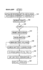
stable AC
power to the PWM controller U1 and the microcontroller 32 during various
operational
conditions including low battery voltage condition as discussed below. In
particular, the
negative polarity side of the primary winding WI is connected to the output of
the
bridge rectifier (Figs 3A and 3B) . A capacitor CY1 is used to improve EMC
performance . The positive polarity side of the primary winding W1 is
connected to
24
CA 02884758 2015-03-10
WO 2014/066345
PCT/US2013/066111
primary side ground PGND (Fig. 3B) by way of a switch Q1 and a parallel pair
of
current sensing resistors R19A and R19B. The switch Ql, implemented as a FET,
is
used to connect and disconnect the positive side of the primary winding W1 to
ground
PGND under the control of variable frequency drive circuit 42 (Fig. 1),
discussed below.
The variable frequency drive circuit 42 causes the switch Q1 to switch
between, for
example, 20 KHz and 100 KHz, for example, as a function of the load current.
1[0062] When the switch Q1 (Fig. 3B) is closed, the primary winding W1 is
connected to the DC output of the bridge rectifier. This causes primary
current to flow
through the primary winding W1 which builds up the magnetic flux and energy in
the
transformer T1. During this condition, a voltage is induced in the secondary
windings
W4 and W5 (Fig. 3C) of the transformer Ti. During this time, a diode D8 (Fig.
3B),
connected between the negative polarity of the primary winding W1 and the
output of
the bridge rectifier, is off. While the switch Ql(Fig. 3B) is closed, the
diode D6 (Fig.
3C) , connected to the positive polarity of the secondary winding W5, will
also be off,
thus preventing an output capacitor C4 from charging. The diode D13, diode D14
and
D16 will be on because the windings W2 and W4 have the same polarity as
winding
W1. Thus, capacitor C7, C8 and C20 will be charged.
[0063] When the switch Ql(Fig. 3B) is open, the diode D8 turns on to clamp
the
voltage spike, caused by the leakage inductance of the transformer Ti, to a
safe level
for the FET through the resistor R10 and the parallel resistors R5A and R5B
and the
capacitor C5. This causes positive voltages across the bias winding W3 and the
secondary winding W4, which, in turn, turns on the diode D5 (Fig. 3B) allowing
the
capacitor C8 to be charged to supply power to Ul; this also turns on the diode
D6 (Fig.
CA 02884758 2015-03-10
WO 2014/066345 PCT/US2013/066111
3C) allowing the output capacitor C4 to charge and supply load current to the
battery.
The diode D7 is also turned on which provides power to the relay RLY1 by way
of a
resistor R31. With power to the relay RLY1, the relay contact is able to close
allowing
current to be delivered to the battery when microcontroller 32 sends a signal
to turn on
the transistor Q5. A diode 015 may be connected across the relay RLY1 to act
as a
snubber during switching of the relay RLY1. The relay is under the control of
a relay
control signal Relay Ctr by way of a resistor R32 and a switch Q5_
[0064] The battery charger output terminals VID+ and Vb- 25 are connected
in
parallel across the output capacitor C4, which supplies the load current to a
battery cell
(not shown) connected to the battery charger output terminals Vb+ and Vb" 25
when the
switch Q1 is closed. When the switch Q1 is open, the secondary winding W5
through
diode D6 charges the output capacitor C4 and supplies the load current to the
battery
as well. As discussed in more detail below, the on and off times of the switch
Q1 are
controlled by the variable frequency drive circuit 42 , discussed below.
Variable Frequency Drive Circuit
[0065] The variable frequency drive circuit 42 (Fig. 1) is illustrated in
Figs. 3B and
3C and includes a PWM controller U1, for example, a Fairchild Model SG6859A
PWM
controller for flyback converters. Other PWM controllers are also suitable.
The PWM
controller Ul includes a green mode function which decreases the switching
frequency
under light load and no-load conditions. The feedback circuit 43 consists of a
voltage
feedback circuit and a current feedback circuit. The voltage feedback circuit
is formed
by the resistor R21, zener diode ZD1 and an opt-coupler U2. The voltage
feedback
26
CA 02884758 2015-03-10
WO 2014/066345 PCT/US2013/066111
circuit limits the Vin voltage to the predetermined value, for example, 16.2V.
The
current feedback circuit is formed by the current sensing resistors RI IA and
RI1B, the
capacitors C3, C9 and C19, the resistors R14, R22, R50 and R27, an operational
amplifier U4A, a diode d10, and an opt-coupler U2. The opt-coupler U2 combines
the
voltage feedback signal and current feedback signal together, then sends it to
the pin
FB of the PWM controller U1. Once the feedback signal at pin FB of U1 exceeds
a
threshold, the switching frequency decreases in order to conserve power during
light
load and no load conditions. For the above mentioned PWM controller, Ul, the
frequency can vary between 20 KHz and 100 KHz. decreasing the switching
frequency
dramatically reduces power consumption.
[0066] The current feedback circuit includes a difference amplifier U4A
(Fig. 3C)
and an opto-coupler U2 (Fig. 3C) connected to a feedback pin FB (Fig. 3B) of
the PWM
controller U1. The difference amplifier U4A (Fig. 3C) compares the voltage of
the
current sensing resistor RI IA, which represents the charging current with a
reference
signal. In this case, the reference signal is formed by the PWM Ctr signal,
which comes
from the microcontroiler 32, through the RC filter circuit consisting of the
resistor R27
and a capacitor C3. The output of the difference amplifier U4A is applied to
the opto-
coupler U2.
[0067] The PWM controller U1 (Fig. 3B) optionally includes a "green-mode
function", for example, as provided by way of a Fairchild Model SG6859A PWM
controller or equivalent. The green mode function causes the PWM to
automatically
reduce the frequency of the switching of the switch 01 as a function of the
load current.
At relatively low load current conditions, the frequency of the PWM controller
U1 is
27
CA 02884758 2015-03-10
WO 2014/066345 PCT/US2013/066111
reduced. At no-load conditions, the frequency is reduced further by a skipping
number
of switching cycles. Reducing the frequency and eliminating cycles of the
switching of
the switch Q1 reduces the power losses.
[0068] As mentioned at above, the high frequency charger circuit 22 has two
control modes, voltage control mode and current control mode. Before the
microcontroller 32 closes the relay RLY1 (Fig. 3C), the high frequency Charger
22
works in the voltage control mode. In this mode, the resistor R21 is serially
connected
to zener diode ZD1. The serial connection is connected between the output of
the
difference amplifier U4A and the positive battery voltage Vb. Since the relay
RLY1 is
open, there is no current from the high frequency charger 22 to battery, the
voltage of
the amplifier U4A (Fig. 3C) is low, which causes diode 010 to be off, Thus
only
resistor R21 senses the voltage Vin and applies the voltage feedback signal
through
ZD1 to opt-coupler U2. Whenever the Vin voltage is higher than the
predetermined
value, for example 16.2V, the zener diode ZD1 will turn on, which ,in turn,
turns on the
opt-coupler U2, which adjusts the voltage at FB pin of the PWM controller 42.
In this
way, the Vin voltage is maintained at the predetermined value, so called
voltage control
mode. When the relay RLY1 closes, a charging current flows to the positive
battery
terminal Vb+ and returns from the negative battery terminal Vb-. The current
sensing
resistors R11A and R11B sense the charging current and send the current signal
to the
non-inverting pin 3 of the amplifier U4A through the RC filter which is
consist of resistor
R22 and capacitor C19. The amplifier U4A compares the charging current signal
at pin
3 with a target charging current setting at the inverting input pin 2 of U4A
which comes
from the signal marked as "PWM Ctr" from the microcontroller 32 through the
28
CA 02884758 2015-03-10
WO 2014/066345
PCT/US2013/066111
connector CN1, the RC filter which consists of the resistors R27 and R50 and
the
capacitor C3. If the charging current signal at pin 3 of U4A is higher than
the target
charging current, at pin 2 of U4A, which is set by the microcontroller 32, the
output
voltage at pin 1 of U4A becomes high, the diode D10 turns on, which, in turn,
adjusts
the voltage at FB pin of the PWM controller 42. Thus, the charging current is
maintained at the target charging current set by the microcontroller 32 when
the
charger is in the current control mode. Since the voltage of a 12V battery is
lower than
the predetermined voltage Vin which is decided by the voltage control mode,
thus the
voltage control mode is inactive during the current control mode. A capacitor
C10 is
also connected to the feedback pin FB of the PWM controller U1 for voltage
stabilization.
[0069] The PWM controller 42 has two different operation modes according to
the
voltage level at its FB pin. They are "Green Mode" and "Normal Mode". When the
voltage at FI3 pin of the PWM controller 42 falls in a certain range, for
example, 2.2 volt
¨ 2.8 volt, the PWM controller enters "Green Mode". Within the Green Mode, the
operating frequency of the PWM controller declines linearly as the voltage at
FB
increases due to the charging load declining. Thus the power losses at the
switcher
FET Ql, the transformer T1 and the output diode D6 decline as the PWM
frequency
decreases, and it leads to higher efficiency at light load conditions. As the
charging
load increases, the voltage at FB pin of the PWM controller decreases. When
the
voltage at FB pin falls below a certain voltage specified by the PWM
controller 42, for
example, 2.2 volt, the PWM controller 42 enters into "Normal Mode", it means
the
29
CA 02884758 2015-03-10
WO 2014/066345
PCT/US2013/066111
PWM controller will work at the maximum operation frequency predetermined by
resistor R18..
[0070] A capacitor C19
(Fig. 3C) is connected to the non-inverting input terminal
of the difference amplifier U4A and ground OGND to filter the noise from the
charging
current signal. Another capacitor C9 is connected between the inverting
terminal of the
difference amplifier U4A and the output and forms a negative feedback loop
used to
stabilize the output voltage of the difference amplifier U4A.
[0071] The power supply terminal Vcc (Fig. 38) of the PWM controller Ul is
connected across the output of the bridge rectifier by way of a pair of
serially
connected resistors R6 and R9 and a capacitor C8. The ground terminal GND on
the
PWM controller U1 is connected to the positive side ground PGND. A resistor
R18 is
connected to the RI pin of the PWM controller U1 to create a constant current
source
and determine the nominal switching frequency. A current sense pin CS senses
the
voltage across the resistor R19A and R198 through resistor R17, connected to
the
positive polarity side of the flyback winding W3 through FET Q1 for over-
current
protection. The resistor R17 forms a voltage divider with the resistor R15.
The CS pin
is also connected to ground POND by way of a capacitor C11. A gate drive pin
GDR is
connected to the gate of the switch 01 by way of a resistor R13 and parallel
diode D9.
Low Voltage Operation
[0072] The hybrid
battery charger 20 allows normal operation down to very low
battery voltages, for example down to 1.0 volts DC. In particular, the power
supply
CA 02884758 2015-03-10
WO 2014/066345 PCT/US2013/066111
voltage for the microcontroller 32 (Fig. 4B, 4C, 4E and 4F) is derived from a
voltage,
identified as Va (Fig. 3C). During conditions when the battery is deeply
discharged, for
example down to 1 volt DC, the discharged battery essentially shorts out the
secondary
winding W5 and dissipates the energy stored in the transformer. During
conditions
when the secondary winding is shorted out, the bias winding W3 will also
effectively be
shorted out because it has the same polarity as the secondary winding W5.
[0073] Normally, the voltage supply Va for the microcontroller 32 (Figs 4B,
4C,
4E and 4F) would normally be powered from the secondary winding W5 by way of
the
diode D7 (Fig. 3C). When the secondary winding W5 is shorted by a deeply
discharged battery, the voltage Va becomes too low to maintain the supply
voltage of
3.3 volt DC for the microcontroller 32 to cause the microcontroller 32 (Figs
4B, 40, 4E
and 4F) to likely perform erratically. For the same reason, the bias winding
W3 cannot
maintain a high enough voltage on capacitor C8 causing the PWM controller U1
to
also not operate normally..
[0074] In order to solve this problem, a pair bias windings W2 and W4 with
the
opposite polarities to winding W3 and W5 are used to provide the proper power
supply
voltage to the microcontroller 32(Figs 4B, 4C, 4E and 4F) and the PWM
controller Ul
(Fig. 3B) during a condition when the battery is deeply discharged. In
particular, the
winding W3 (Fig. 3C) is connected to a diode D5 (Fig. 3B) and a serially
coupled
resistor R4 that will be coupled to the power supply pin VCC of the PWM
controller Ul.
Similarly, the winding W2 is coupled to a resistor R35 and a diode D13 also
coupled to
the power supply pin VCC of the PWM controller U I . The power supply pin VCC
of the
PWM controller U1 is coupled between a pair of serially coupled resistors R6
and R9
31
CA 02884758 2015-03-10
WO 2014/066345
PCT/US2013/066111
and ground by way of a capacitor C8. During conditions when the secondary
winding
W5 of the transformer Ills shorted out, the bias windings W2 and W4 still get
power
from the primary winding Wl, so that the PWM controller U1 and microcontroller
32
can keep working normally.
[0075] During the time the PWM drive pulse goes high, the FET Q1 turns on
connecting the non-dot terminal of the primary winding W1 to the positive rail
of the DC
voltage at capacitor C2. This causes a current flowing from the non-dot
terminal to the
dot terminal of the winding W1, which, in turn, induces currents flowing out
of the non-
dot terminals at winding W2, W3, W4 and W5, respectively. Considering the
polarity of
the diode at each winding, only the diodes D13, D14 and D16, which are
connected to
winding W2 and W4, respectively, will turn on to enable charging of the
capacitors C8,
C7 and C20. The diodes D5 and D6, which are connected to windings W3 and W5
respectively, will be off. The windings W2 and W4 are so called "Forward
Windings",
while the windings W3 and W5 are known as "Flyback Windings". Since the diodes
05
and 06 are off, the induced energy will be stored in the flyback windings W3
and W5
during the period of the FET Q1 on. When the PWM controller U1 turns off the
drive
pulse, the FET Q1 will turn off disconnecting Q1 from the DC voltage at the
capacitor
C2. Thus, the forward windingsW2 and W4 will lose power also, and the diodes
D13,
D14 and D16 will turn off. Meanwhile the energy stored in the flyback windings
W3 and
W5 during FET Q1 on, will force the diodes 05 and 06 to be forward biased and
turn
on the two diodes, thus providing charging currents to the capacitor C8 and C4
respectively. In summary, in one PWM cycle, during the PWM drive pulse high,
the
PWM controller Ul gets power from the winding W2 through the resistor R35,
diode
32
CA 02884758 2015-03-10
WO 2014/066345 PCT/US2013/066111
D13 and the capacitor C8 and the bias source Va to the control circuit . The
microcontroller 32 gets power from the winding W4 through diode 014, resistor
R7 and
capacitor C7. During the PWM drive pulse low, the PWM controller U1 gets power
from
winding W3 through the diode 05, the resistor R4 and the capacitor C8; while
the bias
source Va gets power from winding W5 through diode 06, resistor R26, diode D7
and
capacitor C7. Thus, there are two paths to feed power to the PWM controller U1
and
the bias power Va respectively. So even when the high frequency charger 22 is
shorted by deeply discharged battery, which means the PWM controller U1 and
the
bias power Va will lose one power path which is through winding W3, diode 05,
resistor R4 and capacitor C8 and through winding W5, diode D6, resistor R26,
diode
07 and capacitor C7 respectively, but they can still get power from another
path and
keep working correctly.
[0076] The operational amplifier U4A provides current limiting. In other
words,
during conditions when the battery is deeply discharged, the operational
amplifier U4A
exports a high signal to the opt-coupler U2 through the diode 010 and the
resistor R14
If the charging current to the battery is more than the value set by
microcontroller 32,
the voltage FB pin of PWM controller U1 will reduce the PWM duty cycle, and
the
charging current is limited to the setting value. =
[0077] As shown in Fig. 4A, the voltage Va is used to generate a 3.3 volt
DC
supply voltage for the microcontroller 32 (Figs. 46, 4C, 4E and 4F) . The
voltage of the
regular U3 is controlled by the resistors R53 and R56. In this case, the
regulator U3
generates 3.3 volts, which is applied to the VDD input of the microcontroller
32 (Figs.
4B, 4C, 4E and 4F). The voltage Va, for example 15 volts DC, is applied to the
emitter
33
CA 02884758 2015-03-10
WO 2014/066345 PCT/US2013/066111
of a transistor Q6 (Fig. 4A). A bias resistor R26 is connected between the
base and
emitter of the transistor Q6. The transistor Q6 is under the control of a
transistor Q11,
which, in turn, is under the control of the microcontroller 32 (Figs. 4B, 4C,
4E and 4F)
by way of a current limiting resistor R34 (Fig. 4A) and a load resistor R31.
During
normal operation, the LED display D3 and most of the LEDs LED7-LED1717 are
off.
To save energy consumption, the transistor Q11 and Q6 are turned off by
microprocessor PC1, then the voltage regulator U3 is only connected to Va
through
resistor R27. Since the value of resistor R27, for example, 1KO, is relatively
high, it
limits the current to the voltage regulator U3, in turn, saves energy
consumption. When
users want to turn on the LED display D3 and other LEDs, the switches SW3 or
SW4
are depressed. The microprocessor PC1 needs more power from the 3.3V voltage
regulator U3 to do so. If the 3.3V regulator U3 still only gets power from
resistor R27,
the power will be not enough to supply the microprocessor PC1 and other LEDs.
When
the microprocessor PC1 detects that the switches SW3 or SW4 are depressed, it
turns
on the transistor Q11 (Figs. 4B, 4C, 4E and 4F). The transistor Q11 (Fig. 4A),
in turn,
turns on the transistor Q6, thus connecting the voltage Va to the capacitor
C7. Now the
voltage Va is applied to an adjustable precision shunt regulator U3 not only
by way of
the resistor R27 but also by of a resistor R32 which value is much smaller
than resistor
R27. Thus the voltage regular U3 gets more power from Va to meet the need of
more
power to the microprocessor PC1 and the LEDs.
Flyback Transformer Construction
34
CA 02884758 2015-03-10
WO 2014/066345 PCT/US2013/066111
[0078] As mentioned above, the flyback transformer Ti includes a pair bias
windings W2 and W3, and bias winding W4. These windings are used to provide
power
to the microcontroller 32 as well as the PWM controller U1 during conditions
when the
battery voltage is relatively low, for example, 1.0 volts DC. As discussed
below, the
windings are identified as set forth below.
________________________________ 4.. ________
lAW1 NP1 Primary
W2 NP3 Primary/Bias
W3 NP4 Primary/Bias
W4 NS1 Secondary/Bias
W5 NS2 Secondary
'/2W1 NP2 Primary
[0079] Exemplary construction drawings of the fly back transformer Ti are
illustrated in Figs. 8A and 8B. Referring first to Fig. 8A, the flyback
transformer Ti may
include two (2) primary windings NP1 and NP2 , two bias windings NP3 and NP4
and
two (2) secondary windings NS1 and NS2. The bias winding NP4 is wound on first
at
one end of the bobbin in multi-strands wire to cover the full winding width of
the bobbin
in one layer, thus this bias winding works as a shielding layer to improve EMC
performance. In addition, the main primary winding is wound next and in
opposite
winding direction to this flyback bias winding NP4. It improves the EMC
performance
further. Since this bias winding NP4 is the one which most closest to the
ferrite core of
CA 02884758 2015-03-10
WO 2014/066345
PCT/US2013/066111
the transformer T1 and acts as a ECM shielding, it blocks the noise, created
in the the
primary winding W1, to reach the transformer core, in turn, reduces EMC noise.
Further, the most noisy terminal 2 of the primary winding W1 is arranged to
wound face
to the most quiet terminal 5 which is connected to the ground PGND (Fig. 3B,
3C), this
improves EMC performance further. All windings are wound with the polarities
as
shown in Fig. 8A. In this case, the primary winding W1 is split into two
portions, NP1
and NP2, which will be explained in details next section. . In particular, One
winding
NP3 is connected with the same polarity as the primary winding W1 and the
other
winding NP4 is connected in the opposite polarity. Similarly, secondary
winding NS2 is
connected with the same polarity as the primary winding W1 and the other
secondary
bias winding NS2 is connected in the opposite polarity. This configuration
allows the
primary bias windings NP3 and NP4 and the secondary bias winding NS2 to supply
sufficient voltage to the PWM controller U1 and the microcontroller
respectively even if
the battery voltage is low.
[0080] A winding diagram is shown in Fig. 8B illustrating an exemplary
configuration of the windings on a bobbin. As shown, the primary winding W1 is
split
into two portions, NP1 and NP2. A secondary winding NS1 is sandwiched between
the
half primary winding NP1 and another half primary winding NP2. In this way,
the
leakage inductance between the primary winding W1 and the secondary winding
NS1
is reduced largely, which, in turn, reduces the voltage spike to the FET Q1
when FET
Q1 is turned off. An insulation tape may be disposed between the winding NP3
and the
secondary windings NS1 and NS2. The secondary windings NS1 and NS2 are
36
CA 02884758 2015-03-10
WO 2014/066345
PCT/US2013/066111
connected between the 9 and 10 and 9 and 7, respectively. An insulated tape is
=
disposed between the primary winding NP1 and the bias winding NP4.
[0081] Magnet wire is used for the primary windings NP1 and NP2 and the
bias
windings NP3 and NP4. Triple insulated wire is used for the secondary windings
NS1
and NS2. The specifications for the transformer Ti are set forth below.
[0082] Material List
= Ferrite Core
= Bobbin
= Magnet Wire
= Triple Insulated wire
= Insulation Tape
[0083] Winding Specification
= N P4 : 9 turns of 4x #32 magnet wire (4x =4 wires in parallel), one
layer, start 6
at far side 5.
= NP1: 27 turns of 2x #29 magnet wire, two layers, start 2 3.
= NS1: 9 turns of 2x #22 triple insulated wire, two layers , start 10 ¨>9.
= NP2: 27 turns of 2x #29 wire, two layers, start 3 -41
= NS2: 4 turns of ix triple insulated wire, one layer, spread out, start 9 -
+ 7.
= NP3: 4 turns of lx #32 magnet wire on the same layer as NP3, start 5 (far
side)
¨4.
Microcontroller Control
37
CA 02884758 2015-03-10
WO 2014/066345 PCT/US2013/066111
[0084] The microcontroller 32 (Figs. 4B, 4C, 4E and 4F) may be a Model No.
STM8S003K3T6 microcontroller, available from STMicroelectronics with 8Kbytes
of
flash memory, 1 kilobyte of RAM and 128 bytes of EEPROM. The microcontroller
32
controls a three digit display D3 (Fig. 4c) by way of a plurality of
transistors Q10, Q9
and Q7 and biasing resistors R33, R30 and R28, respectively. The transistors
Q10, Q9
and Q7 are under the control of MUX signals MUX 3, MUX2 and MUX1 which connect
the anodes of the LEDs forming the display to a 3.3 volt DC. The cathodes of
the
LEDs forming the display are connected to the output ports are connected to
the output
ports PD7, P06, P05, PD4, PD3, PD2 and PDO on the microcontroller 32 by way of
the
resistors R38, R39, R40, R41, R42, R43, R44 and R45, respectively. These
output
ports PD7, PD6, P05, PD4, PD3, PD2 and PDO control the operation of the LED
display.
[0085] The microcontroller 32 also controls a number of LEDs as shown in
Fig.
40 . For example, the microcontroller 32 controls the LEDs; LED7, LED8, LED9,
LED10, LED 11, LED 12, and LED 13 by way of a transistor Q8, a biasing
resistor R25
and an input resistor R29. A MUX4 signal from the microcontroller 32 is
applied to the
input resistor R29 to connect a 3.3 volt DC voltage to the anode of the LED7,
LED8,
LED9, LED10, LED 11, LED 12, and LED 13. The cathodes of the LED7, LED8, LED9,
LED10, LED 11, LED 12, and LED 13 are connected to the output ports PD7, PD6,
PD5, PO4, PD3, PD2 and PDO on the microcontroller 32 by way of the resistors
R38,
R39, R40, R41, R42, R43 and R44, respectively. . These ports PD7, P06, PD5,
PD4,
PD3, P02 and PDO control the operation of the LED7, LED8, LED9, LED10, LED 11,
LED 12, and LED 13.
38
CA 02884758 2015-03-10
WO 2014/066345 PCT/US2013/066111
[0086] The microcontroller 32 also controls the LEDs; LED 14 (Fig. 4F), LED
18
and LED 16. These LEDs are connected to output ports PC3, PC2 and PC1 on the
microcontroller by way of the transistors Q12, Q13 and Q14, load resistors
R48, R49
and R51 and the input resistors R50, R52 and R36. Similarly, the
microcontroller 32
controls the LEDs; LED17 and LED15. A voltage of 3.3 volts DC is connected to
the
anodes of the LEDs, LED17 and LED15 by way of a pair of resistors R46 and R47,
respectively. The cathodes of the LEDs, LED 17 and the LED 15 are applied to
the
output ports P64 and P65, respectively.
[0087] The microcontroller 32 also monitors various switches, such as the
switches SW3 (Fig. 4A) and SW4. These switches SW3 and SW4 are connected
between ground and the output ports PB3 (Fig. 4E) and PB2, respectively.
[0088] A scaled amount of the battery voltage is applied to an input port
P60 of
the microcontroller 32. The battery voltage is scaled by a voltage divider
formed from
the resistors R35 and R54. A diode D4 is connected between the resistors R35
and
R54 and 3.3 volts DC. A diode D5 is connected in parallel with the resistor
R54. This
analog voltage at the port PBO is then converted to a digital value by an
analog to
digital converter onboard the microcontroller 32. When the scaled value of the
battery
voltage exceeds 3.3 volts, the diode D4 conducts so that the scaled voltage is
clamped
to 3.3 volts in order to protect the port PBO from damage by over-voltage. The
diode
05 is to protect the port PBO from damage when a reversed polarity battery is
connected to the charger circuit, it also protect the microprocessor from
damage by a
static electric discharge.
39
CA 02884758 2015-03-10
WO 2014/066345 PCT/US2013/066111
[0089] The ground pin VSS is connected to the reset pin NRST by way of a
capacitor C8 and connected to digital ground. The reset is held in a high
logic state by
way of a 3.3 volt DC voltage and a pull-up resistor R37. The VDD pin is the
digital
power supply pin. A 3.3 volt DC voltage is applied to the VDD pin. A capacitor
C9
connected between the VDD pin and the digital ground stabilizes the input
voltage to
the microcontroller 32. A capacitor C10 is connected between a regulator
capacitor pin
Vcap and digital ground. Programming of the microcontroller 32 is by way of
the SWIM
port PD1.
[0090] Output control signals generated by the microcontroller 34 are set
forth in
the table below.
Signal Name Port Pin Number
MUX3 PA3 7
MUX4 PF4 8
FAN Ctr PB6 10
Relay Ctr PCB 23
Phase Ctr. PC5 22
PWM Ctr. PC4 21
[0091] Inputs to the microcontroller 32 are set forth in the table below.
Signal Name Port Pin Number
Current PB1 15
Zero Crs PE5 17
CA 02884758 2015-03-10
WO 2014/066345
PCT/US2013/066111
Battery Voltage PBO 16
[0092] Connections between the microcontroller 32(Figs. 48, 4C, 4E and 4F)
and
the electronic circuitry are by way of 10 pin connectors CN1 (Fig. 3G) and CN2
(Fig.
4A).
[0093] The microcontroller 32 (Figs. 4B, 4C, 4E and 4F) has multiple low
power
modes. For example, the microcontroller 32 may have wait, active halt and halt
low
power modes as set forth below. For a STMicroelectronics , Model STM8S003K3T6
microcontroller, these modes are defined in their STM8S003K3 / STM8S003F3
application data sheet, DOCIDO1 8576, Rev. 3:
= Wait mode: In this mode, the CPU is stopped, but peripherals are kept
running.
The wakeup is performed by an internal or external interrupt or reset.
= Active halt mode with regulator on: In this mode, the CPU and peripheral
clocks are stopped. An internal wakeup is generated at programmable intervals
by the auto wake up unit (AWU). The main voltage regulator is kept powered on,
so current consumption is higher than in active halt mode with regulator off,
but
the wakeup time is faster. Wakeup is triggered by the internal AWU interrupt,
external interrupt or reset.
= Active halt mode with regulator off: This mode is the same as active halt
with
regulator on, except that the main voltage regulator is powered off, so
the
wake up time is slower.
41
CA 02884758 2015-03-10
= WO
2014/066345 PCT/US2013/066111
= Halt mode: In this mode the microcontroller uses the least power. The CPU
and
peripheral clocks are stopped, the main voltage regulator is powered off.
Wakeup
is triggered by external event or reset.
[0094] Another important feature is the ability to place the
microcontroller 32
(Fig. 4B, 4C, 4E and 4F) in a halt or sleep mode. In this mode, the
microcontroller 32
consumes the least amount of power. The microcontroller 32 can be woke up by
applying a reset. This can be done by applying a signal to the NRST pin by way
of the
connector J2 (Fig. 4B). A switch press can be used to wake the microcontroller
32.
Alternatively, a signal from an internal clock timer can be used.
[0095] The microcontroller 32 is programmed by a SWIM pin (Fig. 4C) on
the
microcontroller 32. The SWIM pin on the microcontroller 32 is connected to the
SWIM
pin 3 on the header J2
Fan Control
[0096] In order to provide cooling to the battery charger 20, a fan M2
(Fig. 3D)
may be provided. The fan M2 may be a 12 volt DC fan connected to Vin and
ground
OGND by way of a transistor Q7. A Fan Ctr signal is applied to the input of
the
transistor Q7 by way of an input resistor R48. Anytime the Fan Ctr. signal is
high, the
fan M2 is turned on. A diode 020 is connected across the fan M2 to protect the
transistor Q7 from the back EMF generated when the motor M2 is switched off by
providing a current path through the diode D20 and the motor M2.
Software Control
42
CA 02884758 2015-03-10
WO 2014/066345 PCT/US2013/066111
[0097] Exemplary software control diagrams are illustrated in Figs. 7A-7L.
The
Main Loop is illustrated in Fig. 7A. Initialization of the hybrid charger 20
is illustrated by
the block 100. On power-up of the hybrid charger 20, the system is
initialized.
Initialization includes setting input/output ports, initializing the
analog/digital converters,
initiating the clock and the watchdog timer and initializing interrupts and
system
variables. After initialization, a burn in test is conducted in step 120. The
burn in test
entails simulating a battery charge for a predetermined period of time, for
example 20-
30 minutes, in order to screen out problems not detected during a factory test
[0098] After the burn in step, the system enters a loop 120 which includes
the
steps 120-136. These steps 120-136 are continuously repeated while a battery
is being
charged.
[0099] Initially, the watchdog timer is reset in step 124. Next in step
126, the
charge rate switch SW3 (Fig. 4) and the battery type switch SW4 are read by
the
microcontroller 32 to determine the selected battery type and the selected
charge rate.
Next in step 124, the battery voltage is read from port PBO. After the battery
voltage is
read in step 124, the system checks the battery connection in step 130. The
battery
connection is based on the battery voltage that is read in step 124. If the
battery
voltage is greater than a predetermined value, for example, 0.2 volts DC, the
system
assumes a battery is connected to the battery charger output terminals Vb+ and
Vb-
25 . If the voltage is less than 0.2 volts DC, the system assumes no battery
is
connected and the system loops back to step 124 and reads the battery voltage
again.
The system will loop between steps 128 and 130 until a voltage of at least 0.2
volts Dc
is read. Once the system determines that a battery is connected to the battery
charger
43
output terminals Vb+ and Vb- , the system proceeds to the charge handler in
step 132
and charges the battery. As indicated in the block 132, the charge handler is
illustrated
in Figs 7A-7J. After the charger handler routine is executed, the system
determines in
step 134 the status of the battery charging by measuring the battery voltage
and
charging current and comparing it with the values on the voltage and current
nominal
charging curves, for example, as illustrated in Figs. 2 and 3 to determine the
current
point on those curves of the battery and using that point to determine the
percentage
complete of the battery charging. Once the battery charge percentage is
determined, it
is displayed on the display 03 (Fig. 4) in step 136 by a display handier, and
the LED17
is illuminated to indicate a percentage complete of the battery charging is
being
displayed.
[001001 As mentioned above, the charge handler is illustrated in Figs 7A-
7J.
Referring initially to Fig. 7B, the charge handler is in an initial state at
step 138. In the
initial state INIT_state, the Triac Q4 (Fig. 3F) or alternatively SCRs 04 and
Q8 (Fig. 5)
are turned off. The LEDs, LED 7-LED 18 (Fig. 4), are turned off. The fan M2 is
also
turned off. The system then switches to a CHECK_BATT state, as illustrated in
Fig. 7B.
[001011 Turning to Fig. 7C, once the system enters the CHECK BAIT state,
the
battery voltage is checked in step 140 to determine if it is greater than, for
example, 0.2
volts DC. Each loop through the main loop, the battery voltage is measured
during a
predetermined time period, for example, 3 seconds. Thus, each loop through the
main
loop, a Total Charge Timer or 3 second timer is initialized. If the battery
voltage is less
than, for example, 0.2 volts DC, a 3 second timer is reset and the system
exits
indicating that no battery is attached. If the battery voltage is greater than
0.2 volts DC,
44
CA 2884758 2019-11-08
CA 02884758 2015-03-10
WO 2014/066345 PCT/US2013/066111
the system assumes a battery is connected to the battery charger and
illuminates the
Connected LED 14. If the voltage is equal to or greater than , for example,
17.0 volts
DC, as indicated by the block 144, the system assumes the battery is fully
charges and
resets the 3 second timer in step 142 and then exits and illuminates the
Charged LED
16. Alternatively, if the battery voltage is less than 17.0 volts DC, the
system checks in
step 146 to determine if the 3 second timer has expired which indicates that a
new loop
through the main loop is to be initiated, If the 3 second timer has not
expired, the
system proceeds to step 148 and turns on the Charging LED 18 (Fig. 4), turns
on the
Fan M2 (Fig. 3) by way of the Fan Ctr. Signal, available at the PB6 port (Fig.
4) of the
microcontroller 32. The battery voltage is saved as the variable Vorg. The
system also
clears the Total Charge Timer , i.e. 3 second timer and sets the appropriate
charge as
set by the switch SW3 (Fig. 4A).
[00102] Three different charge rates are selectable by the switch SW3,
namely
SLOW, MEDIUM and FAST charge rates as well as START, which refers to starting
current. If a FAST charge rate is selected both the high frequency charger
circuit 22
(Fig.1) and the linear battery charger circuit 24, are connected in parallel
to the battery
terminals 25. Assuming the linear battery charging circuit 24 can produce an
exemplary
amps DC and the high frequency battery circuit can produce an exemplary 2 amps
DC, a full 12 amps DC can be delivered to a battery in this mode, which
incidentally
defines the fourth mode of operation discussed above.
[00103] During this mode, the relay contact RLY1 is closed connecting the
high
frequency charger circuit 22 to the battery charger output terminals 25. In
this mode,
the microcontroller 32 provides a control signal "Relay Ctr." which controls a
transistor
CA 02884758 2015-03-10
WO 2014/066345 PCT/US2013/066111
Q5, which, in turn, controls the relay RLY1 so as to connect the linear
charger circuit
24 to the battery charger output terminals 25 during this mode.
[00104] During a FAST charge rate or fourth mode of operation, the
microcontroller 32 sends a "Phase Ctr." signal to the triac Q4 (Fig. 3F) or
alternatively
the SCRs Q4 and Q8 (Fig. 5) at the appropriate time to supply the proper
charging
current to the battery to be charged.
[00105] If a MEDIUM charge rate is selected by the switch SW3 (Fig. 4),
only the
linear charger circuit 24 is used to charge a battery connected to the battery
charger
output terminals 25. During this mode, identified above as the second mode,
only the
linear battery charger circuit 24 is connected to the battery charger output
terminals 25.
The high frequency battery charger circuit 22 is disconnected from the battery
charger
output terminals 25 by way of a relay contact RLY1 under the control of a
relay RLY1,
which, in turn is under the control of a transistor Q5. The transistor Q5, in
turn is
controlled by a signal "Relay Ctr." from the microcontroller 32. During this
mode, the
linear battery charging circuit 24 provides battery charging current to the
battery to be
charged, as mentioned above.
[00106] If a SLOW charge rate is selected, only the high frequency charger
circuit
22 is connected to the battery charger output terminals 25 during this mode of
operation, identified above as a third mode of operation. During this mode of
operation,
the triac Q4 (Fig. 3F) or alternatively the SCRs 04 and Q8 (Fig. 5) are off
disconnecting the linear battery charging circuit 24 from the battery charger
output
terminals 25, The relay contact RLY1 is closed in the manner discussed above,
46
CA 02884758 2015-03-10
WO 2014/066345 PCT/US2013/066111
connecting the high frequency charger circuit 22 to the battery charger output
terminals.
[00107] If a START rate is selected by the switch SW3, the linear battery
charging
circuit 24 is connected to the battery charger output terminals 25 in the
manner
mentioned above under the control of the microcontroller 32 (Fig 1) to provide
starting
current, for example 75 amps DC. for a predetermined time, for example, 5
seconds,
under the control of the microcontroller 32. During this mode the relay
contact RLY1
may be open to disconnect the high frequency charger 24 from the battery
output
terminals 25 during this mode.
[00108] Once the charge rate is selected, the system proceeds to the
appropriate
charge algorithm, as mentioned above, and the appropriate charge rate LED is
illuminated. The LED7 corresponds to a slow charge rate. The LED8 corresponds
to a
medium charge rate while the LED9 corresponds to a fast charge rate. The LED10
corresponds to starting current.
[00109] The system also checks the position of the switch 8W4 with respect
to the
battery type. Depending on the position of the switch SW4, the LED
corresponding to
the selected battery type will be illuminated. The LED 12 corresponds to AGM
batteries
while the LED 13 applies to GEL batteries. The system then proceeds to the
START_CHARGE State, as illustrated in Fig. 7D.
[00110] In order to improve the overall efficiency of the hybrid charger,
the linear
battery charging circuit 24 and the high frequency battery charger circuit 22,
the system
takes advantage of the conditions in which these charger circuits are most
efficient, for
example, when one or more of the following exemplary conditions exist:
47
CA 02884758 2015-03-10
WO 2014/066345 PCT/US2013/066111
= the charging current being drawn by the battery is above an exemplary
predetermined value, for example, approximately 7 Amps DC;
= the battery voltage is below a certain value, for example, 13.2 Volts DC,
and
= the rate of change of voltage (dV/dt) is below a predetermined value, for
example, approximately 0.1V/hour.
[00111] During conditions when the linear battery charger circuit 241s in
use,
either alone or in conjunction with the high frequency charger circuit 22,
i.e. FAST and
MEDIUM charge rate conditions, the system monitors various parameters, such as
battery voltage, charging current and the rate of change of voltage with
respect to time,
dV/dt . If any of these parameters meet or exceed the values mentioned above,
for
example, the linear battery charging circuit 24 is switched off, as mentioned
above, and
charging is continued by the high frequency charging circuit 22 to improve the
efficiency of the hybrid charger. Turning to Fig. 7D, for the selected
charging rate, in
step 150, the battery voltage is read and the PWM duty cycle to the linear
charger 24 is
read to regulate the charging current to the selected charging rate. Initially
a first timer,
for example, a 1 minute timer is initiated in step 152. During this minute, a
constant
charging current is applied to the battery and the system checks for a
"sulfation"
condition. Battery sulfation is known to occur when a battery will not accept
a charge.
As such, during the first minute, the battery charging current is limited to a
relatively
low value, for example, 1 amp DC. In step 154. After charging the battery at a
constant
current for a short time period, the system checks the battery voltage to
determine if it
has increased. If not, the system assumes the battery is sulfated in step 156
and
48
CA 02884758 2015-03-10
WO 2014/066345 PCT/US2013/066111
switches to a Desulfation Mode in step 158 and exits. Alternatively, if the
battery
voltage increased during the low level charge, the system assumes the battery
is not
sulfated, the system exits. After the first timer times out, the system checks
in step 160
whether the battery voltage is greater than a predetermined voltage, for
example, 10
volts DC. If the battery voltage is less than the predetermined voltage. If
not , the
system checks a second timer, for example a 120 minute timer, in step 162 to
determine if the battery was charged at the limited charging current and the
second
timer timed out and the battery voltage was still < 10 volts DC. If so, the
system
proceeds to an ABORT state in step 164. If the second timer has not timed out,
the
system exits.
= [00112] If in step 160, the battery voltage is determined to be >
10 volts DC, the
system proceeds to step 166 (Fig. 7E). In step 166, the system checks the
battery
= voltage to determine if the battery voltage is at its nominal level. If
so, the system
proceeds to step 168. In step 168, the system saves the PWM duty cycle and
sets a
third timer, for example, a 60 minute timer, and switches from a constant
current mode
to a constant voltage mode. During a constant voltage mode, the system
monitors the
rate of change of the charging current di/dt and proceeds to a di/dt state.
[00113] Alternatively, if the system determines in step 166 that the
battery voltage
is not at its nominal value, Winish, the system checks in step 170 whether the
battery
voltage is > a first predetermined value, for example, 14.2 volts. If the
battery voltage is
greater than the predetermined voltage, the battery voltage is checked at
periodic
intervals, for example , every 30 minutes in step 172. After every interval,
the system
checks whether the battery voltage has improved in step 174. If not, the
system
49
CA 02884758 2015-03-10
WO 2014/066345 PCT/US2013/066111
checks in step 176 whether the battery voltage has dropped below a second
predetermined value, for example, 14.7 volts DC. If not, in step 178, the
system sets
the variable Vfinish to the predetermined value. The duty cycle is saved and
the third
timer is set. The system also switches to the di/dt state, as illustrated in
Fig. 7F.
[00114] If it is determined in step 170 that the battery voltage is less
than the first
predetermined value, e.g. 14.2 volts, the system checks the battery voltage at
predetermined intervals, for example, every 120 minutes, in step 180. After
every
interval, the progress is checked in step 182. If there is progress, the
system exits and
proceeds to the di/dt state. If there is no progress, the system proceeds to
step 184,
which is the same as step 178.
[00115] The di/dt state is illustrated in Fig. 7F. Initially, in step 186,
the battery
voltage is regulated at %nisi, . The di/dt is determined by checking the pulse
width of the
charging current in order to regulate the battery voltage at Vfinish = As
such, the system
checks in step 188 whether the new duty cycle (DC) is < the old duty cycle. If
not, the
system checks in step 190 whether the new duty cycle is > greater than the old
duty
cycle + a predetermined value, for example 10. If not, the system checks in
step 192
whether the third timer, i.e. 30 minute timer, has timed out. If the system
determines in
step 192 that the third timer did not time out, the system exits and proceeds
to the
MAINT_State. If the third timer has timed out the system proceeds to step 194.
In
step 194, the Charging LED18 (Fig. 4) is turned off and the Charged LED16 is
turned
on. In addition, the system proceeds to the MAINT_State.
[00116] The duty cycle in the constant voltage mode is also used to
determine a
thermal runaway condition. In particular, if it is determined in step 190 that
the new
CA 02884758 2015-03-10
WO 2014/066345
PCT/US2013/066111
duty cycle is > the old duty cycle + the predetermined number, i.e. 10, the
system
assumes a thermal runaway condition in step 196. During this condition, the
system
turns off the Charging LED18 (Fig. 4) and turns on the Charged LED16. The
system
then proceeds to the MAINT_State.
[00117] In step 188, if the system determines the new duty cycle is less
than the
old duty cycle, the system sets old duty cycle variable Old DC equal to the
new duty
cycle variable New DC in step 198. The system proceeds to step 200 and checks
the
charging current. Exemplary charging curves are illustrated in Figs 2 and 3.
As shown
on these figures, the minimum charging current is about 0.4 amps DC. The
system
compares the charging current with the minimum known charging current to
determine
if the charging current is equal to or less than the minimum charging current
If the
charging current is < than the known minimum charging current, the system
assumes
the battery is fully charged and proceeds to step 194. If the charging current
is not <
the minimum current, the system exits and proceeds to the MAINT_State.
[00118] The MAINT_State is illustrated in Fig. 7G. During this state the
battery
voltage is regulated at VmAINT in step 202 by applying a small maintenance
charging
current to the battery. In step 204, the system checks whether the maintenance
charging current is greater than or equal to a predetermined value, for
example, 1.0
amp DC. If not the system exits and proceeds to a MAINT2_state. If the
charging
current is greater than the predetermined value, the system proceeds to step
206. In
step 206, the system initiates a fourth timer, for example, a 12 hour timer,
and
proceeds to the MAINT2_state.
51
[00119] The MAINT2_state is illustrated in Fig. 711. In step 208, the
system
continues to regulate the battery voltage at VmAINT by applying a maintenance
charging
current. In step, 210, the system measures the charging current to determine
if it is
greater than or equal a predetermined value, for example, 1 amp DC. If the
maintenance charging current is determined to be greater than or equal to the
predetermined value, the system limits the maintenance charge current to the
predetermined value in step 212, i.e. 1 amp DC. The system continues charging
the
battery at the limited maintenance charging current until the fourth timer,
i.e. 12 hour
timer, times out as determined in step 214. If the fourth timer has not timed
out, the
system exits and proceeds to the Desulfation state. If the fourth timer has
timed out,
the system proceeds to an Abort state in step 216.
[00120] The Destination state is illustrated in Fig. 71. Initially in
step 218, the
system checks the fourth timer to determine if more than 10 hours, for
example, have
elapsed. If more than 10 hours have elapsed, the system switches to the Abort
state at
step 226. If not more than 10 hours have elapsed, the charging current is
limited to a
second predetermined value, for example, 3 amps DC, in step 220. Next, the
system
checks whether the battery voltage is less than a predetermined value, for
example,
13.8 volts DC, in step 222. If the battery voltage is > than the predetermined
value, the
system exits and proceeds to the Abort State. Alternatively, if the battery
voltage is <
than the predetermined value, the system proceeds to step 224. In step 224,
the
Charging LED18 (Fig. 4) is turned off and the fourth timer, e.g. 12 hour timer
is reset.
The system returns to the Start_ Charge state, illustrated in Figs 7D and 7E.
52
CA 2884758 2019-11-08
[00121] The Abort_state is illustrated in Fig. 7J. In this state, the
triac 04 (Fig. 3)
or alternatively, the SCRs Q4 and Q8 (Fig. 5) are turned off. In addition, the
charging
t_ED18 and the Charged LED16 are turned off.
[00122] A timer interrupt service routine for the Phase Ctr. PWM (Fig. 3)
is
illustrated in Fig. 7K. The interrupt service routine is used to periodically
determine the
duty cycle of the charging current. Initially, all Phase Ctr. PWM interrupts
are cleared
in step 230.
[00123] The Phase Ctr. PWM interrupts are generated by the
microcontroller 32
(Fig. 4B, 4C, 4E and 4F) in order to sense the duty cycle of the charging
current.
Assuming the linear charger 24 (Fig. 3F) is on, the duty cycle is obtained by
the
microcontroller 32 by measuring the pulse duration and the frequency of the
charging
current pulse train. The duty cycle is the ratio of the pulse duration to the
pulse period.
The pulse period is 1/pulse frequency. The duty cycle is determined in terms
of a count
or ticks of a timer.
[00124] In step 232, the variable Phase Ctr. PWM is set to be equal to
the total
Phase Ctr. PWM count minus the duty cycle, as measured. In step 234 the
variable
Phase Ctr. PWM count is incremented by 1. If the Phase Ctr. PWM count is not
less
than the total count, as determined in step 234, the system assumes the
battery is
charged and proceeds to step 242 and turns the triac 04 (Fig. 3F) or the SCRs
04 and
08 (Fig. 5) off. Alternatively, if the Phase Ctr. PWM count is less than the
total Phase
Ctr. PWM count at step 236, the system proceeds to step 238 to determine if
the
Phase Ctr. PWM count is greater than the low duty cycle LDC, the system
assumes
the battery is not
53
CA 2884758 2019-11-08
fully charged. As such, in step 240, the system turns on the triac Q4 (Fig. 3)
or
alternatively the SCRs Q4 and 08 (Fig. 5).
[00125] Fig. 7L illustrates the zero crossing interrupt service routine for
controlling
the triac 04 (Fig. 3) or alternatively the SCRs Q4 and 08 (Fig. 5), as
discussed
above. At every zero crossing the triac 04 or alternatively the SCRs 04 and Q8
are
off, as indicated in step 242. The Phase Ctr. counter is then reset in step
244.
[00126] Obviously, many modifications and variations of the present
invention are
possible in light of the above teachings. Thus, it is to be understood that,
within the
scope of the appended claims, the invention may be practiced otherwise than as
specifically described above.
54
CA 2884758 2018-07-16