Note: Descriptions are shown in the official language in which they were submitted.
WO 2014/047470
PCT/US2013/060980
ENVELOPE FEEDBACK INTERFERENCE REDUCTION AND
DATA THROUGHPUT MAXIMIZATION
BACKGROUND
Field of the Invention
The present invention relates to interference reduction, and more
specifically, to
. envelope feedback interference reduction associated with signal separation.
Background
Communications engineers face a number of challenges today, including
maximizing the amount of information that can be communicated over the limited
resources available. With limited frequencies available over which to
communicate radio
signals, and with the amount of information that people wish to communicate
growing
rapidly, it is important to use the available frequencies as efficiently as
possible.
Unfortunately, for a variety of reasons, the available frequencies are often
interfered with,
causing the loss of valuable frequency space. This is an issue that causes
hundreds of
millions of dollars in financial losses to the satellite industry alone.
One way by which interference can be reduced is to put as much separation as
possible between each pair of potentially interfering signals. Such separation
may be, for
example, by separating the signals by frequency, physical distance, or the
like. However,
separating signals in these ways can reduce the amount of information that can
be
transmitted between a transmitter and a receiver, because the efficiency with
which
information can be transmitted over the communication system may be
diminished.
SUMMARY
The present invention provides for envelop feedback interference reduction
with
signal separation to reduce the impact of interference and to enable maximum
data
throughput. The methods are frequency independent.
In one implementation, a method of reducing interference on an input signal
which
includes a desired signal and an interfering signal is disclosed. The method
includes:
processing the input signal in frequency and time domain to separate the
desired signal
from the interfering signal by: characterizing the interfering signal without
a priori
knowledge of characteristics of the interfering signal; generating a clean
copy of a carrier
2784585
CA 2885222 2018-12-20
WO 2014/047470
PCT/US2013/060980
of the input signal using the characterized interfering signal; inverting the
clean copy of
the carrier and correcting for gain and phase; and summing the inverted clean
copy of the
carrier with the input signal to generate an output signal which is
substantially close to the
desired signal, wherein the generated output signal has adequate signal-to-
noise ratio
(SNR) so that it can be processed.
In another implementation, a signal characterization and separation system to
process an input signal, comprising a desired signal and an interfering
signal, in frequency
and time domain to separate the desired signal from the interfering signal is
disclosed.
The system includes: signal characterization unit configured to characterize
the interfering
signal without a priori knowledge of characteristics of the interfering
signal; and a signal
separation unit configured to generate a clean copy of a carrier of the input
signal using
the characterized interfering signal, to invert the clean copy of the carrier
and correct for
gain and phase, and sum the inverted clean copy of the carrier with the input
signal to
generate an output signal which is substantially close to the desired signal,
wherein the
generated output signal has adequate signal-to-noise ratio (SNR) so that it
can be
processed.
In a further implementation, a non-transitory computer-readable storage medium
storing a computer program for reducing interference on an input signal which
includes a
desired signal and an interfering signal is disclosed. The computer program
includes
executable instructions that cause a computer to: process the input signal in
frequency and
time domain to separate the desired signal from the interfering signal by
executable
instructions that cause the computer to: characterize the interfering signal
without a priori
knowledge of characteristics of the interfering signal; generate a clean copy
of a carrier of
the input signal using the characterized interfering signal; invert the clean
copy of the
carrier and correcting for gain and phase; and sum the inverted clean copy of
the carrier
with the input signal to generate an output signal which is substantially
close to the desired
signal, wherein the generated output signal has adequate signal-to-noise ratio
(SNR) so
that it can be processed.
Other features and advantages of the present invention will become more
readily
apparent to those of ordinary skill in the art after reviewing the following
detailed
description and accompanying drawings.
2
2784585
CA 2885222 2018-12-20
WO 2014/047470
PCT/US2013/060980
BRIEF DESCRIPTION OF THE DRAWINGS
FIG. IA is a flow diagram illustrating an envelope feedback interference
reduction
technique in accordance with one implementation of the present invention.
FIG. 1B is a flow diagram illustrating alternative description of the envelope
feedback interference reduction technique as a method of reducing interference
on an
input signal.
FIG. 2 is a detailed functional block diagram of the interference detection
and
signal separation unit in accordance with one implementation of the present
invention.
FIG. 3 is a functional block diagram of an envelope feedback interference
reduction system in accordance with one implementation of the present
invention.
FIG. 4 is a functional block diagram of a blind signal characterization and
signal
separation system configured in accordance with one implementation of the
present
invention.
FIG. 5 is a functional block diagram of an envelope feedback interference
reduction system in accordance with another implementation in which the
location of the
interference detection and signal separation is after the LNA.
FIG. 6 is a functional block diagram of an envelope feedback interference
reduction system in accordance with yet another implementation in which the
location of
the interference detection and signal separation is at the intermediate
frequency (IF) level.
FIG. 7 is a detailed functional block diagram of the interference detection
and
signal separation unit (shown in FIG. 6) in accordance with one implementation
of the
present invention.
FIG. 8A illustrates a representation of a computer system and a user.
FIG. 8B is a functional block diagram illustrating an envelope feedback
interference system to perform envelope feedback interference technique which
can be
hosted on a computer system or in field programmable gate array
(FPGA)/application-
specific integrated circuit (ASIC).
FIG. 9 is a functional block diagram of a system for interference
cancellation.
FIG. 10 is a graphical depiction of signal interference.
FIG. 11 is a flowchart of a method for interference reduction.
FIG. 12 is a flowchart of an example method for interference reduction.
FIG. 13 is a flowchart of another example method for interference reduction.
FIG. 14 is a flowchart of another example method for interference reduction.
3
2784585
CA 2885222 2018-12-20
WO 2014/047470
PCT/US2013/060980
DETAILED DESCRIPTION
As discussed above, separating the signals to reduce interference by frequency
or
physical distance can reduce the amount of information that can be transmitted
between a
transmitter and a receiver. Further, if the interfering signal is from an
unknown (as is
typically the case) or hostile source, separating signals in these ways may
not be possible.
Certain implementations as described herein provide for envelop feedback
interference reduction and data throughput maximization, and associated
"blind" dual-
carrier signal separation and processing. The term "blind" as used in this
context refers to
processing and/or reduction of a signal without a priori knowledge of the
characteristics of
the signal. After reading this description it will become apparent how to
implement the
invention in various implementations and applications. Although various
implementations
of the present invention will be described herein, it is understood that these
implementations are presented by way of example only, and not limitation. As
such, this
detailed description of various implementations should not be construed to
limit the scope
or breadth of the present invention.
In one implementation, the envelop feedback interference reduction (EFIR)
technique has applications in multiple different communications systems
including, but
not limited to: satellite communications signals and satellite command and
control (C2)
links; unmanned aerial vehicle (UAV) line of sight (LOS) and satellite data
links;
shipboard microwave and satellite communications systems; microwave
communications
links; GPS receivers; cellular phone communications links; cable signals; and
any point-
to-point or point-to-multi-point RF systems that are susceptible to
interference (accidental
or intentional). It also can be used to allow -blind" dual-carrier signal
processing that
allows significantly higher data rates to be transmitted through a satellite
transponder or
other fixed RF bandwidth link than single carrier transmission. The term
"blind" as used
in this context refers to processing and/or reduction of a signal without a
priori knowledge
of the characteristics of the signal.
The unique elements of the interference detection and signal separation
technique
include: blindly determining the characteristics of the signals passing
through an amplifier;
separating the wanted signal from a residual which may contain the effects of
interference
and potentially amplifier compression; canceling the effects of an interfering
carrier that
causes both the interference and potentially compression within a receiver
amplifier; and
recovering a signal that is compromised either or both from interference and
compression
due to the operation on the receiver amplifier. Further, combinations of the
above-listed
4
2784585
CA 2885222 2018-12-20
WO 2014/047470
PCT/US2013/060980
elements can be identified as unique elements as well. However, key technical
challenges
in implementing this technique include: separating and creating the canceling
signal in
real-time, especially if there is distortion from the low-noise amplifier
(LNA);
synchronizing the canceling signal with the interfering signal; and closing
the loop fast
enough to cancel out modulated interfering signals, and when necessary,
separating the
target signal from the remainder of the cancelled interfering signal.
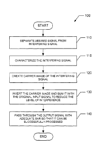
FIG. lA is a flow diagram illustrating an envelope feedback interference
reduction
technique 100 in accordance with one implementation of the present invention.
In the
illustrated implementation of FIG. 1A, the technique 100 separates the desired
signal from
the interfering signal, at box 110. Then, at box 115, the interfering signal
is characterized.
In one implementation, the signal characterization (e.g., box 115) involves
processing the input signal in frequency domain to determine the presence of
the signal
and to determine signal bandwidth and carrier frequency. The carrier frequency
is
measured by measuring the signal raised to an incremental power (e.g., 1, 2,
4, 8, etc.).
That is, the signal is multiplied by itself a number of times until a
continuous-wave (CW)
signal can be seen. Once the frequency measurement is successful, the current
power
index provides a hint about the modulation type (e.g., 1=CW, 2=BPSK, 4=QPSK,
etc.),
even though further measurements may be necessary to disambiguate some
modulations
(e.g., between QPSK and 16QAM). Further, the process also provides a hint
about the
carrier clock rate. Therefore, once the modulation type and the carrier clock
(symbol rate)
are determined, the signal can be reprocessed to measure accurately the
carrier modulation
type and clock rate, which provide the carrier symbol trajectory. In addition
to the
measurement of the carrier, a copy of the residual (interference) carrier is
generated.
The residual signal is reprocessed in the same way as the original input
signal to
separate out the interfering carrier, at box 120, using the carrier symbol
trajectory. The
clean copy of the carrier is then inverted and corrected for gain and phase,
and summed
with the original composite signal, at box 130, to reduce the level of
interference on the
input signal (which originally the interfering signal level was substantially
close enough to
the desired signal to cause processing problems). At box 140, the output
signal is passed
through with adequate signal-to-noise ratio (SNR) so that it can be
successfully processed
(such that the residual signal [interfering signal] level is reduced so that
it does not
materially impact processing of the desired signal).
The envelope feedback interference reduction technique 100 can be
alternatively
described as a method 150 (see FIG. 1B) of reducing interference on an input
signal by
2784585
CA 2885222 2018-12-20
WO 2014/047470
PCT/US2013/060980
creating a clean copy of the most powerful carrier (wanted signal),
reprocessing the
residual carrier to separate out other carriers, determining the wanted signal
and the
unwanted signal and using the unwanted signal (inverted in phase and adjusted
for gain) to
cancel it out via envelope feedback. The method 150 includes: processing the
input signal
in frequency and time domain to separate the desired signal from the
interfering signal, at
box 160; characterizing the interfering signal without a priori knowledge of
the
characteristics of the interfering signal, at box 165; generating a clean copy
of a carrier of
the input signal using the characterized interfering signal, at box 170;
inverting the clean
copy of the carrier and correcting for gain and phase, at box 180; and summing
the
inverted clean copy of the carrier with the input signal, at box 190, to
generate an output
signal which is substantially close to the desired signal, wherein the
generated output
signal has adequate signal-to-noise ratio (SNR) so that it can be processed.
FIG. 2 is a detailed functional block diagram of an interference detection and
signal separation unit 200 in accordance with one implementation of the
present invention.
The unit 200 is configured similarly to an interference detection and signal
separation unit
350 of FIG. 3. In this implementation, the signal including the desired and
interfering
signals is received by a down-converter 260 to convert the RF signal into an
IF signal. A
digitizer 210 digitizes the IF signal and sends the digitized signal to an
interference
detection unit 220, which is configured to detect an interfering signal. A
signal separation
unit 230 is configured to isolate the interfering signal. The output of this
unit 230 is then
fed back into the unit 220 to maintain the loop. The output is also fed into a
signal
regeneration unit 240 to produce clean interfering signal, which is received
by a phase
inversion unit 250 to create a canceling signal. An up-converter 270 converts
the
canceling signal from the IF to the original RF (if required). Although the
unit 200 of FIG.
2 shows the signal being down-converted to IF before it is processed and being
up-
converted back to RF once the processing is done, it should be noted that the
processing
can be done all in RF without the need for down-converter and up-converter.
The down-
converter is only required for high frequency signal (e.g. Ghz signals)
because of
limitation in the speed of current digitizers, such that they can only
digitize up to Mhz
frequencies. The methods are frequency independent and (with current digitizer
technology) applications of signals in the hundreds of megahertz and below
will not
require any frequency conversion).
FIG. 3 is a functional block diagram of an envelope feedback interference
reduction system 300 in accordance with one implementation of the present
invention.
6
2784585
CA 2885222 2018-12-20
WO 2014/047470
PCT/US2013/060980
This implementation takes into account compression from the LNA because of an
overdrive condition caused by the interfering signal. The system 300 is
designed to
address the key challenges of separating and creating the canceling signal in
real-time,
synchronizing the canceling signal with the interfering signal, and closing
the loop fast
enough to cancel out both continuous wave and modulated interfering signals.
Accordingly, the system 300 includes an antenna 310 which receives an input
signal (see
370) including desired and interfering signals, and an interference detection
and signal
separation unit 350 (the design of unit 350 may be similar to that of unit 200
of FIG. 2) to
detect the interfering signal and subtract it from the input signal.
The design of an envelope feedback interference reduction system may vary
depending on the location of the interference detection and signal separation
unit. For
example, the interference reduction system will be substantially similar to
the design of
the envelope feedback interference reduction system 300 shown in FIG. 3, when
the
location of the interference detection and signal separation is around the LNA
330. This
configuration will be useful for applications where the LNA will be saturated
by the
interfering signal causing distortion of the output of the LNA. The signal
distortion will
impact the desired signal, such that the canceling signal must be removed
before the LNA
to prevent the distortion. Thus, the effects from the distortion will need to
be taken into
account in the creation of the canceling signal. No delay circuit can be used,
which means
that the speed of the feedback circuit will drive what type of signal that can
be cancelled,
and will limit the applicability of this configuration to allow operations
through
interference.
FIG. 4 is a functional block diagram of a "blind" signal characterization and
signal
separation system 400 configured in accordance with one implementation of the
present
invention. The system 400 is configured similarly to the interference
detection and signal
separation unit 350 of FIG. 3. In the illustrated implementation of FIG. 4,
the system 400
includes a data windowing unit 410, a clock generator 412, a Fourier transform
unit 420, a
decision unit 430, a re-sampling unit 440, and an adaptive regenerative unit
450. The data
windowing unit 410 and the clock generator 412 are configured to receive the
raw signal
and process it in time domain to band limit the signal.
The data windowing unit 410 (window data to correct bandwidth) is configured
to
process the signal in the frequency and time domain to determine the presence
of the
signal and to determine signal bandwidth and center frequency. The Fourier
transform
unit 420 and the decision unit 430 are configured to process the signal in
time domain to
7
2784585
CA 2885222 2018-12-20
WO 2014/047470
PCT/US2013/060980
determine the modulation characteristics, and accurately measure the carrier
frequency by
measuring the signal raised to an incremental power (e.g., 1, 2, 4, 8, etc.).
That is, the
signal is multiplied by itself a number of times until a continuous-wave (CW)
signal can
be seen. Once the frequency measurement is successful, the current power index
provides
a hint about the modulation type (e.g., 1=CW, 2=BPSK, 4=QPSK, etc.), even
though
further measurements may be necessary to disambiguate some modulations (e.g.,
between
QPSK and 16QAM). Further, the process also provides a hint about the carrier
clock rate.
Therefore, once the modulation type and the carrier clock (symbol rate) are
determined,
the signal can be reprocessed by the re-sampling unit 440 (e.g., an equalizer)
to measure
accurately the carrier modulation type and the clock rate, which enable it to
follow the
carrier symbol trajectory.
The adaptive regenerative unit 450 performs a signal separation task using the
carrier symbol trajectory. That is, the unit 450 generates a clean copy of the
carrier
(wanted signal) using the carrier symbol trajectory. A signal equalizer is
built and clocked
at X times the carrier clock rate. The unit 450 inverts and corrects the clean
copy for gain
and phase and sums it with the original composite signal. The output is the
residual
(interfering) signal, which is adjusted for gain and phase and fed back to the
input of the
LNA. The LNA output signal has a greatly reduced interfering signal such that
LNA
compression is avoided and the SNR is sufficient to allow processing of the
residual
(target) signal. If the target signal is still not adequate but there is at
least 6 db of
separation between the residual signal and the remaining interfering signal
after
cancellation, the signal separation technique can be added to the output of
the LNA to
create a clean version of the residual (target) signal.
Referring back to FIG. 3, the effects of interferences and distortions (see
374) are
canceled in an amplifier 360 and a combiner 320. The amplifier 360 inverts the
residual
signal and corrects for gain and phase. The combiner 320 sums the modified
residual with
the input signal and provides the output to a low-noise amplifier (LNA) 330
(and through
to a coupler 340) to cancel the unwanted signals thus reducing the energy into
the LNA to
eliminate the signal compression. Although the initial attempts may not cancel
all
interferences and distortions, the system 300 will eventually settle to
produce an output
signal (see 372) with substantially reduced interferences and distortions
after several
iterations around the loop. The loops will need to be continuously updated to
track and
correct changes in the interfering signal that may be due to changes related
to it being a
modulated signal, changes to signal level from changes to the transmission
path, and
8
2784585
CA 2885222 2018-12-20
WO 2014/047470
PCT/US2013/060980
changes in frequency due to Doppler or it being a sweeping signal. The speed
at which
the loops can settle will determine the effectiveness of the cancellation. But
with the
separation and regeneration capability at the output, only a 6 db separation
is required to
allow the system to regenerate the residual (target) signal.
FIG. 5 is a functional block diagram of an envelope feedback interference
reduction system 500 in accordance with another implementation in which the
location of
the interference detection and signal separation is after the LNA 520. In this
implementation, it is unlikely that an interfering signal will saturate the
LNA 520, and
there is no signal distortion cause by the amplifier compression. Further, the
signal is not
reduced to an IF signal level, such as on traditional bent pipe communications
satellites, to
deal with uplink interference, or with microwave and cell phone relay/repeater
stations
applications. Thus, this implementation would be applicable where a short
delay in the
transmission is acceptable. Accordingly, the envelope feedback interference
reduction
system 500 includes an antenna 510 which receives an input signal including
desired and
interfering signals, and an interference detection and signal separation unit
550 that is
substantially similar to the unit 200 shown in FIG. 2.
In the illustrated implementation of FIG. 5, the system 500 includes a short
delay
circuit 540 which receives and inserts a short delay in the input signal from
the LNA 520
(through a coupler 530). The effects of interferences and distortions are
canceled in an
amplifier 560 and a combiner 570. The amplifier 560 inverts the residual
signal and
corrects for gain and phase. The combiner 570 sums the modified residual with
the
delayed input signal to cancel the interferences and distortions from the
input signal. The
combiner 570 outputs a desired signal with adequate signal-to-noise ratio
(SNR) so that it
can be successfully processed.
FIG. 6 is a functional block diagram of an envelope feedback interference
reduction system 600 in accordance with yet another implementation in which
the location
of the interference detection and signal separation is at the intermediate
frequency (IF)
level. Thus, in this implementation, the interference detection and signal
separation does
not need RF/IF down- and up- conversion processes. Accordingly, this
implementation is
applicable to all end point RF communication and information receiver systems.
This
implementation is also applicable to blind dual-carrier communications systems
including
radio receivers, satellite terminals/modems, GPS receivers, airborne
(aircraft, UAV,
missiles) line of RF sight communications, maritime/shipboard communications
systems
(satellite and line of sight), cellular phones base stations and receivers,
WiMax receivers,
9
2784585
CA 2885222 2018-12-20
WO 2014/047470
PCT/US2013/060980
microwave radios, and RF over wire, cable, waveguide systems. This
implementation also
includes a short delay circuit 640 in the primary path to allow detecting
signal changes and
responses.
In the illustrated implementation of FIG. 6, the system 600 includes an
antenna 610
which receives an input signal including desired and interfering signals. This
input signal
is passed to the LNA 620, to a down-converter 625, and then to an interference
detection
and signal separation unit 650 through a coupler 630. The system 600 also
includes a
short delay circuit 640 which receives and inserts a short delay in the input
signal from the
down-converter 625. The effects of interferences and distortions are canceled
in an
amplifier 660 and a combiner 670. The amplifier 660 inverts the residual
signal and
corrects for gain and phase. The combiner 670 sums the modified residual with
the
delayed input signal to cancel the interferences and distortions from the
input signal. The
combiner 670 outputs a desired signal with adequate signal-to-noise ratio
(SNR) so that it
can be successfully processed. It should be noted that the interference
detection and signal
separation unit 650 processes the signal in intermediate frequency since the
input signal is
down-converted in the down-converter 625.
FIG. 7 is a detailed functional block diagram of the interference detection
and
signal separation unit 650 (shown in FIG. 6) in accordance with one
implementation of the
present invention. In this implementation, the IF signal including the desired
and
interfering signals is received by a digitizer 710 which digitizes the IF
signal and sends the
digitized signal to an interference detection unit 720, which is configured to
detect an
interfering signal. A signal separation unit 730 is configured to isolate the
interfering
signal. The output of this unit 730 is then fed back into the unit 720 to
maintain the loop.
The output is also fed into a signal regeneration unit 740 to produce clean
interfering
signal, which is received by a phase inversion unit 750 to create an isolated
version of the
canceling signal.
FIG. 8A illustrates a representation of a computer system 800 and a user 802.
In
one implementation, the user 802 uses the computer system 800 to perform
envelope
feedback interference reduction.
FIG. 8B is a functional block diagram illustrating the envelope feedback
interference system 890 to perform envelope feedback interference technique
(e.g., as
illustrated in FIG. IA or FIG. 1B). This technique can be hosted on a computer
system or
in field programmable gate array (FPGA)/application-specific integrated
circuit (ASIC).
The controller 810 is a programmable processor and controls the operation of
the
2784585
CA 2885222 2018-12-20
WO 2014/047470
PCT/US2013/060980
computer system 800 and its components. The controller 810 loads instructions
(e.g., in
the form of a computer program) from the memory 820 or an embedded controller
memory (not shown) and executes these instructions to control the system.
Memory 820 stores data temporarily for use by the other components of the
computer system 800. In one implementation, memory 820 is implemented as RAM.
In
another implementation, memory 820 also includes long-term or permanent
memory, such
as flash memory and/or ROM.
Storage 830 stores data temporarily or long term for use by other components
of
the computer system 800, such as for storing data and program of the envelope
feedback
interference system 890. Storage 830 is sometimes referred to as a computer-
readable
storage medium which stores non-transitory data. In one implementation,
storage 830 is a
hard disk drive.
In its execution, the envelope feedback interference system 890 is loaded into
the
memory 820 or storage 830 as a software system. Alternatively, this service
can be
implemented as separate hardware components (e.g., field programmable gate
array
(FPGA)) in the computer system 800.
The media device 840 receives removable media and reads and/or writes data to
the inserted media. In one implementation, for example, the media device 840
is an
optical disc drive.
The user interface 850 includes components for accepting user input from the
user
of the computer system 800 and presenting information to the user. In one
implementation, the user interface 850 includes a keyboard, a mouse, audio
speakers, and
a display. The controller 810 uses input from the user to adjust the operation
of the
computer system 800.
The I/O interface 860 includes one or more I/O ports to connect to
corresponding
I/O devices, such as external storage or supplemental devices (e.g., a printer
or a PDA). In
one implementation, the ports of the I/O interface 860 include ports such as:
USB ports,
PCMCIA ports, serial ports, and/or parallel ports. In another implementation,
the I/O
interface 860 includes a wireless interface for communication with external
devices
wirelessly.
The network interface 870 includes a wired and/or wireless network connection,
such as an RJ-45 or "Wi-Fi" interface (including, but not limited to 302.11)
supporting an
Ethernet connection.
11
2784585
CA 2885222 2018-12-20
WO 2014/047470
PCT/US2013/060980
The computer system 800 includes additional hardware and software typical of
computer systems (e.g., power, cooling, operating system), though these
components are
not specifically shown in FIG. 8B for simplicity. In other implementations,
different
configurations of the computer system can be used (e.g., different bus or
storage
configurations or a multi-processor configuration).
In a further implementation, augmentation to the above-described envelop
feedback interference reduction includes pulsing off the primary signal for
interference
characterization. For example, the primary signal is pulsed off periodically
when
interference is detected or suspected to capture and characterize the
interfering signal.
During the primary signal off period, full measurement characterization of the
interfering
signal is performed. A canceling signal (which removes the interference) is
then
generated by using the measurement characterization of the interfering signal.
For
example, in the presence of suspected interference, the modem could be
operated at a high
duty cycle (e.g., 90%, that is, modem on for 900 milliseconds and off for 100
milliseconds,
for example). During the 100 millisecond off period, the interference is
characterized and
the interference information is used to create a canceling signal that allows
processing of
the primary signal for the remaining 900 milliseconds. The duty cycle and the
duration of
each cycle can be tailored to the application, the rate of change of the
interfering signal
and the speed of the characterization circuit, such that it possible to
foresee (for a highly
dynamic interferer) a 50% duty cycle operating with a total cycle time of 1
millisecond or
even 10 microseconds. In other implementations, the duty cycle and the cycle
duration
can be adjusted to maximize the data throughput based on the rate of change in
the
interfering signal's characteristics and the speed of the characterization
circuit.
The above description of the disclosed implementations is provided to enable
any
person skilled in the art to make or use the invention. Various modifications
to these
implementations will be readily apparent to those skilled in the art, and the
generic
principles described herein can be applied to other implementations without
departing
from the spirit or scope of the invention. Accordingly, additional
implementations and
variations are also within the scope of the invention. For example, although
the
implementations discussed above focus on canceling the interfering signal, the
envelope
feedback interference reduction systems and techniques described above can be
used to
enable cancel each signal individually so that both signals can be processed
allowing for a
blind dual-carrier process to maximize data throughput on an RF system, or to
allow
characterize and capture, but not cancel the interfering signal for real-time
or post process
12
2784585
CA 2885222 2018-12-20
WO 2014/047470
PCT/US2013/060980
analysis. Further, it is to be understood that the description and drawings
presented herein
are representative of the subject matter which is broadly contemplated by the
present
invention. It is further understood that the scope of the present invention
fully
encompasses other implementations that may become obvious to those skilled in
the art
and that the scope of the present invention is accordingly limited by nothing
other than the
appended claims.
13
2784585
CA 2885222 2018-12-20
WO 2014/047470
PCT/US2013/060980
APPENDIX
14
2784585
CA 2885222 2019-01-11
WO 2014/047470
PCT/US2013/060980
Application Areas
= Envelop Feedback Interference
Reduction (EFIR) technique has
applications in multiple different
communication systems
* Including but not limited to:
= Satellite communications signals and satellite Command and
Control (C2) links
UAV line of sight and satellite data link
- Shipboard microwave and satellite communications systems
= Microwave communications links
= GPS receivers
= Cellular phone communications links
= Cable signals
= Basically applicable to any point to point or
point to multi-point RF system that is
susceptible to interference (accidental or
intentional)
/ It also can be used to allow blind
carrier-on-carrier signal processing
that allows significantly higher data
rates to be transmitted through a
transponder than single carrier
transmissions
2784585
CA 2885222 2019-01-11
WO 2014/047470
PCT/US2013/060980
Theory of Operation
Kratos through Sat Corp has been a
leader in interference detection in
satellite and some terrestrial based
systems
= Have existing company proprietary algorithms
that can blindly detect carriers under carriers
and blindly characterize the signals
= Characterization includes Bandwidth, Modulation, data rate,
FEC, etc.
- Capability includes characterization of even signal
underneath
other signals (e.g. lower level interfering signals)
= Building upon our detection
capability to add the ability to
remove or cancel out the
majority of the interfering signal:
= Separate the two signals using company
developed DSP algorithms
= Create a cancelling image of the interfering
signal
- Re-insert the cancelling image signal such that
it greatly reduces the level of the interfering
signal
- Pass through the resulting desired signal with
adequate signal to noise ratio such that is can
be successfully processed
16
2784585
CA 2885222 2019-01-11
WO 2014/047470
PCT/US2013/060980
Theory of Operation
= Key technical challenges:
6 Separating and creating the cancelling signal
in real-time, especially if there is distortion
from the LNA
- Synchronizing the cancelling signal with the
interfering signal
4, Closing the loop fast enough to cancel out
modulated interfering signals, without adding
significant delay in the transmission
17
2784585
CA 2885222 2019-01-11
WO 2014/047470
PCT/US2013/060980
Theory of Operation
Unique elements of this invention
from other signal cancelling
techniques
The invention main themes,
4. Blindly determine the characteristics of the
signals passing through an amplifier.
= Separate the wanted signal from a residual
which contains the effects of compression
and any interference
= Cancel the effects of an interfering carrier
that causes compression within a receivers
amplifier
= Recovers a signal that is compromised both
from interference and compression due to the
operation on the receiver amplifier.
= Targeted uses are for interference removal
and for blind signal-on-signal communication
Other techniques:
^ Are focused on processing both signals in a
single on signal system to maximize data
throughput of a transponder
= Need a copy of one of the signals in order to
cancel or separate the two signals to obtain
the secondary signal
= Do not compensate for amplifier
compression that can occur from
interference, but does not occur from
planned signal-on-signal communication
methods
Assume they won't drive amplifier into
compression
Other techniques known to us are
Doubletalk TM owned by Applied Signal
Technologies (AST) now a division of
Raytheon, and Paired Carrier Multiple Access
(PCMA) owned by Viasat
18
2784585
CA 2885222 2019-01-11
I
WO 2014/047470
PCT/US2013/060980
Theory of Operation
= Example of signal separation and
analysis
0 Blue trace is the wanted signaL
6 Red trace is the interference to be
removed
19
2784585
;
CA 2885222 2019-01-11
WO 2014/047470
PCT/US2013/060980
Theory of Operation
0 Key blocks of blind signal
characterization and signal
separation
2784585
CA 2885222 2019-01-11
WO 2014/047470
PCT/US2013/060980
Theory of Operation
Determine Signal Characteristics
= Signal is processed in the frequency domain
to determine presence of signal and to
determine signal bandwidth and center
frequency
= Signal is processed time domain to band
limit the signal
= First loop at modulation characteristics is
made
= The carrier frequency is measured by
frequency measurement on the signal raised
to incremental power (1,2,4,8,...)
= This is to say that the signal is multiplied by
itself a number of times until a CW signal can
be seen
- Once the frequency measurement is
successful, the current power index gives a
hint about the modulation type (1->CW,2-
>BPSK,4->QPSK) further tests are required to
disambiguate some modulations (QPSK and
16QAM for instance)
= The process also gives hints at carrier clock
rate
- Once modulation type is determined and
carrier clock (symbol rate) is determined, the
signal is reprocessed via an equalizer to
measure accurately the carrier modulation
type and clock rate. Out of this process is an
attempt at following the carrier symbol
trajectory.
21
2784585
CA 2885222 2019-01-11
I
WO 2014/047470
PCT/US2013/060980
. Theory of Operation
= Adaptive Regenerative Technology
(Signal Separation)
* The symbol trajectory is used to create a
clean copy of the carrier
* A signal equalizer is built and clocked at X
times the carrier clock rate
* The clean copy is inverted and corrected
for gain and phase and summed with the
original composite signal
* The output is the residual signal that
represents the effects of interference and
distortions due to amplifier compression
* Cancel the effects of
interference
= The residual signal is itself then inverted
and corrected for gain and phase
= The modified residual is summed with the
input signal to the amplifier to cancel the
unwanted signals.
0 Dynamic Loop
* The first attempts will includes errors,
that will become less so as iterations
around the loop continue to process the
signal and cancel the effects of
compression and interference.
')2.
2784585
r
CA 2885222 2019-01-11
WO 2014/047470
PCT/US2013/060980
Theory of Operation: Location
of Cancellation Around the LNA
1.Around the Receiver LNA cancellation
For applications where the LNA will be
saturated by an interfering signal causing
distortion of the output of the LNA
Signal distortion will impact the desired signal,
such that the cancelling signal must be removed
before the LNA to prevent the distortion.
Effects from the distortion will need to be taken
into account in the creation of the cancelling
signal
No delay circuit can be used, which means that
the speed of the feedback circuit will drive what
type of signal that can be cancelled
= i.e. will not work for signals changing too rapidly
= This will limit the applicability of this method to
allow operations through interference
Fortunately, LNAs are typically
amplifying low power signals and as
such have significant margin to
saturation
Cases where the LNA saturation will
occur is typically with CW, sweeping
or regular pulse signal type
interference
23
2784585
CA 2885222 2019-01-11
WO 2014/047470
PCT/US2013/060980
Theory of Operation: Location
of Cancellation Post LNA
2.Post Low Noise Amplifier (LNA)
cancellation
= For applications where:
It is unlikely that an interfering signal will saturate the
LNA and no signal distortion is occurring
The signal is not reduced to an IF signal level, such as:
= On traditional bent pipe communications satellites to deal
with uplink interference
= Microwave and cell phone relay/repeater stations
applications
= Applications where a short delay in the transmission is
acceptable
= Design includes a short delay circuit within
the ART primary path to allow the cancelling
circuit to detection signal changes and
response
= Operation is still at the original RF input
frequency
= These are usually cause my modulated
signals
= Delay will be needed to handle the changes associated
with the modulation
= But for many applications, delays as large as even a
second are acceptable
24
2784585
CA 2885222 2019-01-11
WO 2014/047470
PCT/US2013/060980
Theory of Operation=. Location
of Cancellation At IF
3.Cancellation at IF
= For receiver applications where the signal
will be processed
Design is simplify by not needing RF/IF down and
upconversion
Design includes a short delay circuit in the primary path to
allow the cancelling circuit to detection signal changes
and response
= This is applicable to all end point RF
communication and information receiver
systems, as well as how blind carrier-on-
carrier communications system would use
this technology
= Radio receivers
= Satellite terminals/modems
= GPS receivers
= Airborne (aircraft, UAV, missiles) line of RF sight
communications
Maritime/Shipboard communications systems (satellite
and line of sight)
= Cellular phones base stations and receivers
= WiMax receivers
= Microwave radios
Also applicable to RF over wire, cable, waveguide systems
= Broadcast video distribution
2784585
CA 2885222 2019-01-11