Note: Descriptions are shown in the official language in which they were submitted.
CA 02885367 2015-03-18
WO 2014/067645
PCT/EP2013/003240
10 Contact element for transmitting high-frequency signals between two
circuit
boards
The invention relates to a r;ontact element for the electrically conductive
connection of contact regions situated in opposite position's and in
particular to a
contact element by which radio-frequency signals can be transmitted between
two
components, and in particular two printed circuit boards, with as great a
freedom
from losses as possible. The invention also relates to a contact device having
a
plurality of such contact elements.
Contact elements of this kind are intended to ensure that the radio-frequency
signals are transmitted with as great a freedom from losses as possible, even
within a defined range of tolerances where the tolerances are on the
parallelism of
the two printed circuit boards and on the axial distance between them. Even a
radial offset between the contact-making regions is to be compensated for if
required. Further requirements to be met by contact elements of this kind lie
in the
areas of inexpensive manufacture and, where necessary, easy fitting. Also, the
axial and radial dimensions of the contact elements are to be as small as
possible.
It is known for a connection to be made between two printed circuit boards by
means of two co-axial insertion-type connectors which are solidly connected to
the
printed circuit boards and an adapter, the so-called "bullet", which connects
the
two co-axial insertion-type connectors. This adapter allows an axial and
radial
compensation for tolerances and also allows tolerances on parallelism to be
CA 02885367 2015-03-18
WO 2014/067645 2
PCT/EP2013/003240
compensated for. Typical co-axial insertion-type connectors used for this
purpose
are SMP connectors, mini-SMP connectors and FMC connectors.
Alternatively, electric connections are also made between two printed circuit
.. boards by means of spring-loaded contact pins of single-conductor and/or
multi-
conductor construction.
Also, there is known from US 6,776,668 B1 a co-axial contact element via which
radio-frequency signals are to be transmitted between two printed circuit
boards.
In this case a centre conductor, in the form of a spring-loaded contact pin,
acts as
a signal conductor, while an outer conductor surrounding the centre conductor
performs the functions of a return conductor and of shielding for the centre
conductor. The outer conductor comprises a base body in sleeve form which is
slotted more than once in the longitudinal direction. At its end-face, the
unslotted
end of the base body forms a point of contact to make contact with a contact-
making region of one of the printed circuit boards. Displaceably guided on the
base body is a sleeve of the outer conductor which at one end, at its end-
face,
forms a point of contact to make contact with a contact-making region on the
other
printed circuit board. A pre-loaded spring is supported between the base body
and
the sleeve. As the two printed circuit boards are being connected, both the
head of
the centre conductor, which centre conductor is in the form of a spring-loaded
contact pin, and the sleeve of the outer conductor are displaced and thereby
subject their respective springs to further pre-loading, whereby secure and
reliable
contact-making pressure can be produced in spite of any possible tolerances on
the distance from one another of the contact-making regions of the printed
circuit
boards. Because the base body is slotted, it also has a certain flexibility in
the
lateral direction, what is intended to be achieved thereby being the ability
to
compensate even for relatively large degrees of non-parallelism between the
two
contact-making regions.
Also known is the use of simple resilient tongues as contact elements or as
parts
of contact elements. These have the advantage of being easy to construct and
inexpensive to manufacture as, for example, stamped, punched or die-cut, and
W020141067645 3
PCT/EP2013/003240
bent, components. At the same time, resilient tongues perform all the
essential
functions of contact elements of this kind, namely on the one hand the
= transmission of power or signals, and also the elastic deformation to
obtain an
adequate contact-making pressure at the points of contact and to compensate
for
tolerances on the attitude and position of the components to be connected.
What
is disadvantageous .however is that, due to their principle, resilient tongues
extend
along an arcuate or angled path and the contact-making regions to be connected
electrically are thus not connected in a direct line. The relatively great
length of the
resilient tongue goes hand in hand with a relatively high impedance and even
inductance, which may have an adverse effect in particular on the quality of
the
transmission of radio-frequency signals.
Taking the above prior art as a point of departure, the object underlying the
invention was to specify an improved contact element for the electrical
connection
of components. In particular, this connecting element was to be distinguished
by
good transmission of radio-frequency signals, properties which compensated for
tolerances, and/or inexpensive manufacture,
The idea underlying the invention is to improve a contact element in the form
of a
resilient tongue by providing ¨ as well as the path of connection through the
resilient tongue itself - an additional path of connection which connects the
contact-making regions of the components to be connected electrically in as
direct
a line as possible and which is therefore of the shortest possible length.
A contact element according to the invention for the electrically conductive
connection of components therefore has points of contact for making contact
with
said contact-making regions and also comprises a first section which connects
the
CA 2885367 2018-07-10
CA 02885367 2015-03-18
WO 2014/067645 4 1'CT/EP2013/003240
points of contact electrically and which is at least partly in the form of a
resilient
tongue. Also provided is a second section which connects the points of contact
electrically, the path of connection formed by this latter being shorter than
that
formed by the first section.
What is meant by "resilient tongue" for the purposes of the invention is a
component of preferably mainly two-dimensional extent (of a thickness which is
only a fraction of its width and length, with its width preferably also being
only a
fraction of its length) which extends into a free space from a point of
connection at
which it is solidly connected to another component, said component being
deflected elastically when there is a pressure on the area defined by its
length and
width and thus providing a functional resilient action.
The design according to the invention of a contact element creates a path of
connection which is short and which is therefore distinguished by low
impedance.
The inductance of the contact element according to the invention is also
comparatively low, which has a positive effect on the transmission of radio-
frequency signals.
Despite these good electrical properties, it is possible for the contact
element
according to the invention to be distinguished by extremely simple
construction
and the ability to be manufactured inexpensively, in particular as a stamped,
punched or die-cut, and bent, component. This is particularly true when, in a
preferred embodiment, the first section and second section of the contact
element
are integrally formed in the form of one resilient tongue. The contact element
according to the invention may thus take the form of a single resilient tongue
which,
due to its shaping, has a first section which primarily, as a result of
elastic
deformation, ensures the contact-making pressure at the points of contact and
a
compensation for tolerances, whereas a shorter second section acts primarily
to
transmit power or signals.
It must be possible for a relative movement of the points of contact on the
contact
element due to an elastic deformation of the first section to be compensated
for by
CA 02885367 2015-03-18
WO 2014/067645 5
PCT/EP2013/003240
the second section. This may take place as a result of an appropriate elastic
deformation of the second section. Provision is however preferably made for
the
second section to comprise sub-sections which slide against one another when
there is a deformation of the first section. This embodiment may have the
advantage that the length of the path of connection always adjusts to the
actual
distance between the points of contact.
A contact device according to the invention is characterised in that it
comprises a
plurality of contact elements according to the invention.
The contact elements are preferably so arranged in this case that their first
sections surround their second sections (or at least a section or sections
thereof)
annularly. Good contact can be ensured in this way with comparatively large
contact-making regions on the components between which contact is to be made.
Because, when this is case, each point of contact is also able to yield
individually
as a result of a corresponding deformation of the associated first section,
even
comparatively large tolerances (in particular on parallelism) to which the
contact-
making regions to be connected are subject can be compensated for by a contact
device of this kind.
When the contact device is designed as a co-axial contact device in which the
contact elements form an outer conductor which surrounds a centre conductor,
shielding may be produced for the centre conductor by arranging the first
sections
of the contact elements to be of a (preferably circular) annular form.
Particularly to further improve the shielding action performed by the first
sections
of the contact elements, provision may also be made for these latter to be
arranged around the second sections as a double annulus and for them thereby
to
form a double shield to a certain degree. Hence the first sections of a first
sub-set
of the contact elements would surround the second sections of the contact
elements annularly and the first sections of a second sub-set of the contact
elements would surround the first sections of the first sub-set annularly.
CA 02885367 2015-03-18
WO 2014/067645 6
PCT/EP2013/003240
In this case, the first sections of one annulus (which first sections are,
furthermore,
preferably each arranged at a uniform spacing) may be offset in rotation
(preferably by half the spacing) from the first sections of the second
annulus, the
gaps formed between the first sections of an annulus (as seen from the second
sections) thus being hidden (at least partly) by the first sections of the
other
annulus.
In one embodiment of contact device according to the invention, provision may
be
made for at least g section or sections of the second sections of the contact
elements to be formed by a common conductor. This may have advantages
particularly with regard to manufacture and fitting.
Furthermore, provision may be made in this case for the common conductor to be
of a rigid form and to form, at a first end (along the longitudinal axis), a
point of
contact for contact with a first one of the contact-making regions, and for
the
second sections of the contact elements, in the form of resilient tongues, to
be
fastened to the common conductor. The resilient tongues then preferably form
the
points of contact for contact with (at least) one second contact-making
region.
Provision may also be made in this case for the first sections of the contact
elements to project beyond a second end (along the longitudinal axis) of the
common conductor, in which case the points of contact are, furthermore,
preferably formed by the projecting sections of the resilient tongues. When a
contact-making surface with which contact is to be made by the points of
contact
on the resilient tongues lies in a plane, this ensures ensure that adequate
travel in
deformation is provided for the resilient tongues and that the corresponding
second end of the common conductor along the longitudinal axis is prevented
from
coming into contact with the contact-making region.
In an embodiment of contact device according to the invention which is also
preferred, provision may be made for the resilient tongues to rest against (at
least)
one section of the common conductor under spring loading and to be movable
relative thereto.
CA 02885367 2015-03-18
WO 2014/067645 7
PCT/EP2013/003240
In one embodiment of the resilient tongues, provision may also be made for
their
free ends to point in the direction of the first end of the common conductor
(and
hence in the direction of that end of the common conductor to which they are
fastened), and for central sections of the resilient tongues to form the
points of
contact. Furthermore, provision may then preferably be made for the resilient
tongues to rest against the common conductor in the region of their free ends.
In an alternative embodiment of the resilient tongues, provision may be made
for
the free ends of the resilient tongues to point in the direction of the second
end
and for the points of contact to make contact with the associated contact-
making
region to be formed in the region of the free ends. Furthermore, provision may
then be made for central sections of the resilient tongues to rest against the
common conductor.
The possibility does of course exist of both these embodiments of the
resilient
tongues being combined in a contact device according to the invention.
To simplify the manufacturability of a contact element according to the
invention or
a contact device according to the invention, provision may be made for the
resilient tongues of the contact elements to comprise two sections which are
offset
laterally and which overlap in a section along the longitudinal axis and are
connected there (preferably in one piece). This particularly simplifies the
use of a
bending tool when a cage of resilient tongues which creates the resilient
tongues
is being manufactured as a stamped, punched or die-cut, and bent, component.
The contact device according to the invention preferably takes the form of a
co-
axial contact device having a centre conductor and an outer conductor
surrounding the centre conductor. A particular preference in this case is for
provision to be made for the outer conductor to be formed in accordance with
the
invention whereas, as a further preference, the centre conductor may take the
form of a spring-loaded contact pin.
CA 02885367 2015-03-18
WO 2014/067645 8
PCT/EP2013/003240
The contact element according to the invention and the contact device
according
to the invention may advantageously be used to transmit radio-frequency
signals
between components and in particular printed circuit boards, with the centre
conductor preferably being used as a signal conductor and the outer conductor
as
a return conductor and/or shielding in an embodiment as a co-axial contact
device.
The invention is explained in detail below by reference to embodiments shown
in
the drawings. In the drawings:
Fig. 1 is a perspective view of an embodiment of contact element according to
the invention in the unloaded state.
Fig. 2 is a view from the front of the contact element shown in Fig. 1.
Fig. 3 is a view from the side of the contact element shown in Figs. 1 and 2.
Fig. 4 is a view from the front of the contact element shown in Figs. 1 to 3
in the
loaded state.
Fig. 5 is a view from the side of the contact element shown in Fig. 4.
Fig. 6 is a perspective view of a second embodiment of contact device
according
to the invention.
Fig. 7 is a longitudinal section through the contact device shown in Fig. 6.
Fig. 8 is a perspective view of a third embodiment of contact device according
to
the invention.
Fig. 9 is a longitudinal section through the contact device shown in Fig. 8.
Fig. 10 is a perspective view of a fourth embodiment of contact device
according
to the invention.
CA 02885367 2015-03-18
WO 2014/067645 9
PCT/EP2013/003240
Fig. 11 is a longitudinal section through the contact device shown in Fig. 10.
Fig. 12 is a view partly in section of a fifth embodiment of contact device
according
to the invention.
Fig. 13 is a plan view of the contact device shown in Fig. 12.
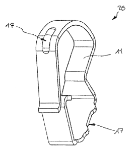
The contact element shown in Figs. 1 to 5 is of a one-piece form in the form
of a
resilient tongue 11 made of electrically conductive material (and in
particular of a
metal). The contact element creates two points of contact 17 which are
intended to
make contact with contact-making regions of two components, and in particular
two printed circuit boards, which are to be connected electrically via one or
more
of the contact elements. One of the points of contact 17 (the one at the
bottom in
Figs. 1 to 5) is comparatively large in area. Via this point of contact 17,
the contact
element is intended to be connected, and in particular soldered or brazed,
solidly
to the associated contact-making region of a component. The second point of
contact 17, which is more of a point or linear form, is intended by contrast
to make
free contact with the associated contact-making region of a component, i.e. to
do
so only under a contact-making pressure exerted as a result of an elastic
deformation of the contact element.
A first section of the contact element, which connects the two points of
contact 17
electrically, is responsible primarily for generating the contact-making
pressure.
Movement towards one another of the points of contact results in an elastic
deformation of this first section, as can be seen in particular in Fig. 5.
A second section comprises two sub-sections each of which comprises one of the
free ends of the resilient tongue 11. On a first, comparatively small,
deformation of
the first section, the two sub-sections come into contact and thus likewise
connect
the two points of contact 17 together electrically. This creates a primary
path for
the radio-frequency signals to be transmitted via the contact element, said
primary
path being appreciably shorter than the path which is formed by the first
section. If
CA 02885367 2015-03-18
WO 2014/067645 10 PCT/EP
2013/003240
there is further deformation of the first section the two sub-sections slide
against
one another. As they do so the length of the path of connection is reduced.
The contact devices shown in Figs. 6 to 11 each comprise a centre conductor 1,
an outer conductor 2 and an insulating member 3 arranged between the centre
conductor 1 and the outer conductor 2.
The centre conductor 1 takes in each case the form of a spring-loaded contact
pin,
i.e. it comprises an electrically conductive sleeve 4 and an electrically
conductive
head 5 having a spherical contact-making surface, part of which head 5 is
guided
within the sleeve 4 to be movable. Arranged inside the sleeve 4 is a spring 6
which
is supported between the head 5 and the floor of the sleeve 4. The centre
conductor 1 is immovably mounted within a receiving opening in the insulating
member 3. The centre conductor 1 may in particular be connected to the
insulator
3 in this case by being physically united therewith, e.g. by adhesive bonding.
The
floor end of the sleeve 4 remote from the head 5 forms a contact-making
surface
which acts as a point of contact 17 to make contact with a contact-making
region
of an underlying printed circuit board (not shown).
The outer conductor 2 comprises in principle a plurality of contact elements
according to the invention and comprises one common conductor 7 which entirely
surrounds the circumferential surface of the insulator 3 and which partly
surrounds
the latter's end-faces. As a result, the common conductor 7 too is immovably
connected to the insulating member 3. As well as this possibility of a
connection by
interengagerhent, provision may also be made, alternatively or in addition,
for a
connection by friction or physical union.
The common conductor 7 comprises a base part 8 and a sleeve part 9 which is
solidly connected thereto (in particular by physical union, e.g. by soldering,
brazing
or welding).
CA 02885367 2015-03-18
WO 2014/067645 11
PCT/EP2013/003240
On the side remote from the insulator 3, the base part 8 forms a contact-
making
surface which acts as a point of contact 17 to make contact with a contact-
making
region of an underlying printed circuit board.
That end of the sleeve part 9 which is connected to the base part 8 comprises
a
surrounding projection 10 to which an electrically conductive cage of
resilient
tongues is fastened (preferably py physical union and in particular by
soldering or
brazing). The cage of resilient tongues creates a plurality (actually eight in
this
case) of resilient tongues 11 which, starting from an annular section 12 which
is
radially directed relative to the sleeve part 9 and via which the cage of
resilient
tongues is connected to the common conductor 7, are distributed around the
circumference of said annular section 12 at a uniform spacing and extend in an
arcuate form in the longitudinal direction of the contact device.
The three embodiments of contact device according to the invention which are
shown in Figs. 6 to 11 differ in the shape of their resilient tongues 11 and
in the
position of the points of contact 17 formed by these latter.
In the embodiment shown in Figs. 6 and 7 the resilient tongues 11 each extend
¨
starting from the outer edge of the annular section 12 ¨ in an almost semi-
circular
arc which merges into a portion angled at approximately 900. In the sections
of the
resilient tongues 11 which follow on from this, in which the latter already
project
beyond the common conductor 7, they extend approximately in parallel. Finally,
the free ends of the resilient tongues 11 are of a form where they are also
bent
outwards. These bent ends form the points of contact 17 by which the outer
conductor 2 is able to make contact with a contact-making region of a target
printed circuit board (not shown), which contact-making region is plane and
aligned substantially perpendicularly to the longitudinal axis of the contact
device.
In those sections of the resilient tongues 11 which extend parallel to one
another,
the latter rest against a surrounding projection 13 (of semi-circular cross-
section)
from the sleeve part 9 of the common conductor 7. They rest in this way under
spring loading, which is applied by the resilient tongues 11 themselves.
CA 02885367 2015-03-18
WO 2014/067645 12
PCT1EP2013/003240
In the embodiment shown in Figs. 8 and 9, the resilient tongues 11 ¨ beginning
from the outer edge of the annular section 12 ¨ first extend through a 900 arc
and
then merge into a section in which they extend almost in parallel.
Approximately
on a level with the upper end of the common conductor 7, this section merges
into
a 1800 arc. The points of contact 17 by which the outer conductor 2 is able to
make contact with a contact-making region of the target printed circuit board
are
situated approximately in the centre of the section forming the 1800 arc. The
resilient tongues 11 rest against the common conductor 7 under spring loading
and this takes place in the region or vicinity of their free ends.
In the embodiment shown in Figs. 10 and lithe resilient tongues extend in a
similar way to those of the embodiment shown in Figs. 8 and 9, although in
this
case there is no central section provided in which they are aligned
approximately
in parallel. Instead, the resilient tongues 11 ¨ beginning from the outer edge
of the
annular section 12 ¨ extend in an arc of more or less continuous curvature
which
extends over approximately 270 .
The resilient tongues 11 of the embodiment shown in Figs. 10 and 11 also
differ
from those of the embodiment shown in Figs. 8 and 9 in their two-dimensional
shape. Whereas the latter are each formed by a single bent strip of
substantially
constant width, the resilient tongues 11 of the contact device shown in Figs.
10
and 11 are of a two-dimensional shape in which two bent sub-strips are
arranged
to be offset laterally, these sub-strips also overlapping in a section along
their
longitudinal axis where they are connected together in one piece. This
embodiment may simplify the manufacture of the cage of resilient tongues as a
stamped, punched or die-cut, and bent, component because each lateral offset
creates space for the entry of a bending tool to do work on one of the sub-
strips.
The contact device shown in Figs. 12 and 13 has resilient tongues 11 which
substantially correspond to those of the contact device shown in Figs. 8 and 9
in
respect of their configuration. A material difference between this contact
device
and that shown in Figs. 6 to 11 is the connection of the common conductor 7 to
a
CA 02885367 2015-03-18
WO 2014/067645 13 PCT/E1"2013/003240
connecting conductor 14 which forms a nut 15 and an outside thread 16. By
means of this outside thread 16, the contact device can be fixed in an opening
in a
housing (not shown). The sleeve 4 of the centre conductor 1 is of a form which
is
lengthened to suit and projects beyond the free end of the connecting
conductor
14.
In the contact devices shown in Figs. 6 to 13, the resilient tongues 11 each
form
part of a first section of a contact element according to the invention. By
means of
them, the two points of contact 17 of the outer conductor 2 of the contact
device
are connected electrically, the primary functions being the generation of a
contact-
making pressure at the upper points of contact and compensation for tolerances
on the attitude and alignment of the contact-making regions of the components
to
be connected. Because the lower point of contact 17 is formed by the underside
of
the base part 8 (or by the connecting conductor 14 in the case of contact
device
shown in Figs. 12 and 13), the base part 8 (or the connecting conductor 14, as
the
case may be), a part of the sleeve part 9, and the annular section 12 are
likewise
part of the first section of each of the contact elements. A second section of
the
individual contact elements, which serves primarily to make the electrical
connection, is formed by the common conductor 7 and the respective parts of
the
resilient tongues 11 which extend between the surrounding projection 13 from
the
sleeve part 9 and the respective points of contact 17 on the resilient tongues
11.
A material advantage of the contact device according to the invention which is
shown in Figs. 6 to 13 is that the path of connection which is formed by the
second
sections of the contact elements forming the outer conductor 2 is always
substantially of exactly the same length as the signal path through the centre
conductor 1, whereby it is possible to obtain a suitably equal signal path.
The distance between the two printed circuit boards between which an
electrically
conductive connection is to be made by means of one or more of the contact
devices shown in Figs. 6 to 13, is preferably selected to be sufficiently
large for
both the centre conductor 1 of the contact device(s) arranged between them and
also the outer conductor 2 thereof to be compressed. Hence, in the first place
the
CA 02885367 2015-03-18
WO 2014/067645 1'CT/EP2013/003240
head 5 of the centre conductor 1 is displaced a short distance towards the
floor of
the sleeve 4 in opposition to the force exerted by the spring 6, which latter
is
thereby pre-loaded to a greater degree, while the resilient tongues 11 of the
outer
conductor 2 are compressed in the direction defined by the longitudinal axis
of the
contact device, which involves a reduction in their radius of curvature, or
rather
their radii of curvature, and hence an increasing pre-loading of the resilient
tongues 11. The intended compression of the contact devices between the
printed
circuit boards is preferably selected not to be so large that the target
printed circuit
board touches the upper edges of the sleeve 4 of the centre conductor 1 or
those
of the sleeve part 9 of the outer conductor 2.
All in all, there is thus provided for both the centre conductor 1 and the
outer
conductor 2 of the contact devices a "resilient travel" in both directions by
which
departures from the desired size of the inter-board distance in both
directions (its
being larger or smaller) can be compensated for. Such departures may, in
particular, be due to tolerances, in which case not only tolerances on
positioning
may be compensated for but also tolerances on attitude, i.e. particularly
deviations
from the intended parallelism between the two printed circuit boards and
between
the contact-making regions arranged thereon which are associated with the
given
contact device. Because of the design according to the invention of the outer
conductor 2 of the contact devices, where there are a plurality of
individually
deformable contact elements, it is also possible for these tolerances on
attitude to
be comparatively large. The point contact which the spherical head 5 of the
centre
conductor 1 makes is likewise insensitive to departures such as were
mentioned.
As the resilient tongues 11 are deformed, a sliding takes place and hence a
relative movement between the sleeve part 9 of the outer conductor 2 and the
resilient tongues 11 at those points at which they are resting against one
another.
In the embodiment shown in Figs. 6 and 7, the points where they rest are
always
on the surrounding projection 13 from the sleeve part 9 of the outer conductor
7.
Depending on the deformation of the resilient tongues 11, said surrounding
projection 13 thus makes contact with different points on the resilient
tongues 11,
provision being made for the resting to take place only within that section in
which
CA 02885367 2015-03-18
WO 2014/067645 15
PCT/EP2013/003240
the resilient tongues 11 extend in parallel. In the embodiments shown in Figs.
8 to
11, the resting points are, by contrast, always formed by the radiused end
sections
of the resilient tongues 11 which, depending on the deformation of the
resilient
tongues 11, touch the outside of the sleeve part 9 of the outer conductor 2 at
different points.
In the embodiments shown in Figs. 8 to 11, provision is also made for the
surrounding projection 13 on the sleeve part 9 of the common conductor 7 to
form
an abutment for the expansion of the resilient tongues 11. In conjunction with
the
component of force which the resilient pre-loading of the resilient tongues 11
in the
radial direction exerts against the sleeve part 4 of the outer conductor 2,
the
resilient tongues 11 are thus able to be held under pre-loading even in the
unloaded state, i.e. when they are not arranged between two suitably spaced
printed circuit boards.