Note: Descriptions are shown in the official language in which they were submitted.
IVIETHODS AND.DrvicEs FOR AC CURRENT SOfiRCF,S, PRECISIQIN
EC ER AN DF.TF CTO
FIELD OF THE INVENTION
[001] This invention relates generally to precision AC current sources,
precision current
transducers, and measurements, which include precision AC current, voltage,
phase,
impedance, frequency, power and energy measurements, over current ranges from
1 mA or
less to 20kA or greater and voltage ranges of 1V or less to 1000kV or greater
and over
frequency ranges from a few hertz to hundreds of kilohertz. In particular it
relates to precision
AC current sources, precision current transducers, and measurements using
enhanced dual
stage current transducers.
BACKGROUND OF THE INVENTION
[002] Alternating Current (AC) electrical measurements are used in a wide
variety of
applications and may be performed for a variety of electrical quantities
including, for
example, voltage, current, capacitance, impedance, frequency, phase, power,
energy, and
resistance. These tests and measurements include those relating to designing,
evaluating,
maintaining and servicing electrical circuits and equipment range from high
voltage electrical
transmission lines operating at hundreds of kilovolts (kV) and kiloamps (kA)
to industrial /
medical / residential electrical and lighting, typically 400V/240V/100V and
30/15A, to a
wide variety of industrial/ scientific/medical/consumer electrical and
electronic devices
operating at voltages of hundreds of mV and currents of a few mA.
[003] Within a variety of AC current applications and AC current test
equipment systems
AC comparator bridges and AC current transformers are employed to provide the
required
- 1 -
CA 2885445 2017-07-10
CA 02885445 2015-03-20
dynamic range, accuracy, and flexibility. AC current bridge configurations
remove inany of
the issues associated with achieving making measurements at accuracies of a
part, or few
parts per million, such as insensitivity to lead resistances, excellent ratio
linearity, excellent
ratio stability, and a high level of resolution. AC current transformers,
importantly, isolate the
measuring instruments from what may be very high voltage in the monitored
circuit and
when the current in a circuit is too high to bc directly applied to measuring
instruments, a
current transformer produces a reduced current accurately proportional to the
current in the
circuit, which can be conveniently connected to measuring and recording
instruments. They
also allow accurate high current generation from precision lower current
sources and isolation
=
of the precision source from external variations.
[005] Accordingly many sources and measurement systems for alternating current
power
systems have a current transformer at their output and input stages
respectively. Over the past
approximately 180 years whilst a wide variety of types of electrical
transformer are made for
different purposes these, despite their design differences, employ the same
basic principle as
discovered in 1831 by Michael Faraday, and share several key functional parts.
Over this
period many techniques have been developed to improve the accuracy of the
current
transformer. Among them, the dual stage current transformer, described in the
work of
Brooks and Holtz in "The Two-Stage Current Transformer" (AIEE Trans., Vol.41,
pp382-
393, 1922) still forins the basis for a significant proportion of commercial
systems. These
transformers arc generally what is referred to as "step down transformers" for
converting
high voltage ¨ low current inputs to lower voltage - higher current outputs.
[006] However, in a range of other applications within electrical systems and
measurement
systems what is required are precision AC current sources and AC amplifiers.
The inventors
have found that improvement of the accuracy when designing a precision AC
current source
is a different problem to measurement systems in that we either wish to remove
measuring
equipment connected to the output circuit to provide the feedback or wish that
the generation
and measurement of even very large current AC current sources is performed
without
requiring the use of a shunt.
[007] Accordingly, the inventors have established design and circuit
methodologies which
are applicable to precision AC current sources, amplifiers, and also AC
current
measurements. Such measurements include precision AC current, voltage, phase,
impedance,
frequency, power and energy measurements, over current ranges from 1mA or less
to 20kA
- 2 -
CA 02885445 2015-03-20
or greater and voltage ranges of IV or less to 1000kV or greater and over
frequency ranges
from a few hertz to hundreds of kilohertz. Similarly, precision AC current
sources and
amplifiers for test, measurement, and supply applications are desirable over
current ranges
from lmA or less to 20kA or greater and voltage ranges of IV or less to 1000kV
or greater
and over frequency ranges from a few hertz to hundreds of kilohertz,
[0081 Other aspects
and features of the present invention will become apparent to those
ordinarily skilled in the art upon review of the following description of
specific embodiments
of the invention in conjunction with the accompanying figures.
SUMMARY OF THE INVENTION
[0091 It is an object of the present invention to provide improvements over
the prior art in
respect of AC precision current sources, amplifiers, and measurements, which
include
precision AC current, voltage, phase, impedance, frequency, power and energy
measurements, over current ranges from lmA or less to 20kA or greater and
voltage ranges
of 1V or less to l 000kV or greater and over frequency ranges from a few hertz
to hundreds of
kilohertz, In particular it relates to precision AC current sources, precision
current
transducers, and measurements using enhanced dual stage current transducers.
[00101 In accordance with an embodiment of the invention there is provided a
device
comprising:
a dual stage current transducer comprising at least a primary winding, a first
secondary
winding and a second secondary winding;
a first four terminal shunt coupled across thc first secondary winding; and
a second four terminal shunt coupled across the second secondary winding;
wherein
a first voltage generated across the second four terminal shunt is subtracted
from a second
voltage generated across the first four terminal shunt.
[0011] In accordance with an embodiment of the invention there is provided a
device
comprising:
a dual stage current transducer comprising at least a primary winding, a first
secondary
winding and a second secondary winding;
a first four terminal shunt coupled across the first secondary winding;
a second four terminal shunt coupled across the second secondary winding;
-3 -
CA 02885445 2015-03-20
an alternating currcnt source disposed between the first secondary winding and
first four
terminal shunt; and
a third four terminal shunt coupled in series with a load across the primary
winding.
[0012] In accordance with an embodiment of the invention there is provided a
method
comprising providing a multi-stage current transducer with a first means to
obtain a first
voltage proportional to a primary current of said multi-stage current
transducer and a second
means to obtain a second voltage proportional to a secondary current in a
second stage of the
multi-stage current transducer, said secondary current being proportional to
the magnetizing
current of the magnetic core of a first stage of the multi-stage current
transducer..
[0013] In accordance with an embodiment of the invention there is provided a
method
comprising:
providing a current transducer having two stages where current of a first
secondary of the
current transduccr passes through a first four terminal shunt and a current of
a second
secondary of the current transducer passes through a second four terminal
shunt;
summing the voltages from the first and second four terminal shunts to
represent the
instantaneous value of the primary current within the current transducer; and
at least one of:
digitizing the resulting summed voltage; and
providing the current transd,¨.er comprises providing a first magnetic core of
the
current transducer in the form of a hollow toroid and a second magnetic core
of thc current transducer in the forni of a toroid core embedded within the
first
magnetic core.
[0014] In accordance with an embodiment of the invention there is provided a
method
comprising providing a bridge for establishing the value of the resistance and
the inductance
of a load, the bridge comprising a current transducer having two stages and
first to third four
terminal shunts, wherein a first current within a first secondary of the
current transducer
passes through a First four terminal shunt, a second current within a second
secondary of the
current transducer passes through a second four terminal shunt and a third
current passing
through the load disposed across a primary of the current transducer also
passes through the
third four terminal shunt.
- 4 -
CA 02885445 2015-03-20
[00151 Other aspects and features of the present invention will become
apparent to those
ordinarily skilled in the art upon review of the following description of
specific embodiments
of the invention in conjunction with the accompanying figures.
BRIEF DESCRIPTION OF THE DRAWINGS
[0016] Embodiments of the present invention will now be described, by way of
example
only, with reference to the attached Figures, wherein:
[0017] Figure 1 depicts an AC current transformer according to the prior art
using a dual
stage current transformer design of Brooks and Holtz;
[0018] Figure 2A depicts a circuit using a dual stage AC current transducer
with electrical
shield and four terminal resistor for improved accuracy;
[0019] Figure 2B depicts a circuit using dual stage AC current transducers
with a
transimpedance amplifier to sum the currents from the first and second stages;
[0020] Figure 3A depicts an AC dual stage current transducer using dual
independent
resistors for improved accuracy according to an embodiment of the invention;
[0021] Figure 3B depicts a precision AC current source exploiting a dual stage
current
transducer, dual independent load resistors, and a programmable controlled
current source
according to an embodiment of the invention;
[0022] Figure 4A depicts a precision AC current source exploiting a dual stage
current
transducer, dual independent load resistors, and with an adjustable
uncontrolled current
source according to an embodiment of the invention transducer;
[0023] Figure 4B depicts a precision AC current source exploiting a dual stage
current
transducer with adjustable uncontrolled current source and a transimpedance
amplifier to sum
the currents from the first and second stages according to an embodiment of
the invention;
[0024] Figures 5A through 5C depict high current AC shunt calibrators
according to
embodiments of the invention exploiting a dual stage current transducers
[0025] Figure 6 depicts dual stage current transducer designs exploiting core-
in-core, dual
core, and triple core designs to provide AC devices according to embodirnents
of the
invention as described in respect of Figures 2A through 5B;
[0026] Figure 7 depicts a dual stage current transducer design exploiting a
core-in-core
design to provide AC devices according to embodiments of the invention as
described in
respect of Figures 2A through 5B; and
- 5 -
CA 02885445 2015-03-20
[0027] Figure 8 depicts a dual stage current transducer design exploiting a
three core design
to provide AC devices according to embodiments of the invention as described
in respect of
Figures 2A through 5B.
DETAILED DESCRIPTION
[0028] The present invention is directed to improvements over the prior art in
respect of AC
precision current sources, precision currcnt transducers, and measurements,
which include
precision AC current, voltage, phase, impedance, frequency, power and energy
measurements, over current ranges from imA or less to 20kA or greater and
voltage ranges
of 1V or less to 1 000kV or greater and over frequency ranges from a few hertz
to hundreds of
kilohertz. In particular it relates to precision AC current sources, precision
current
transducers, and measurements using enhanced dual stage current transducers.
[0029] The ensuing description provides exemplary embodiment(s) only, and is
not intended
to limit the scope, applicability or configuration of the disclosure. Rathcr,
the ensuing
description of the exemplary embodiment(s) will provide those skilled in the
art with an
enabling description for implementing an exemplary embodiment. It being
understood that
various changes may be made in the function and arrangement of elements
without departing
from the spirit and scope as set forth in the appended claims.
[0030] Within the drawings presented in respect of this specification elements
having the
same number are the same element and may or may not be referenced explicitly
in every
drawing due to the recurring elements being commonly numbered.
[0031] Dual stage transformers as known by one of skill in the art comprise
three windings
n.igether with one or more magnetic cores. These three windings are commonly
referred to as
the primary winding, to which the signal to be transformed by the dual stage
transformer is
coupled, the first secondary winding, from which the transformed signal is
coupled, and the
second secondary winding (also known as the correction winding), from which a
signal
(commonly referred to as the correction signal) is coupled. The primary
winding and first
secondary winding may in some embodiments of the dual stage transformer be
conceptually
identical and coupled with the same magnetic flux and can be, for example,
swapped to
reverse the dual stage transformer operation. In contrast the second secondary
winding cannot
be swapped with either of the main windings, namely the primary winding and
first
secondary winding. Within this document, except for the claims and thc summary
of the
-6
CA 02885445 2015-03-20
invention where the terms first secondary winding and second secondary winding
are
maintained, the first secondary winding will be referred to as the "secondary
winding" (with
the current flowing within it referred to as the secondary current) and the
second secondary
winding will be referred to as the correction winding (with the current
flowing within it
referred to as the correction current).
[0032] Referring to Figure 1 there is depicted a dual stage transformer 100
according to the
prior art of Brooks and Holtz, scc "The Two-Stage Current Transformer" (AIEE
Trans.,
Vol.41, pp382-393, 1922). Within this the current transformation is effected
in two stages,
the first generated by secondary winding N, 110B in response to the signal
coupled to the
primary winding N0 110A, which is approximately correct in magnitude and
phase. The
second stage is the generation of an auxiliary corrective current via
correction winding N,
110C which, when combined with the secondary current, gives a resultant
current which very
closely approximates to the secondary current which would be furnished by an
ideal current
transformer having no errors. As depicted the secondary and correction
windings 110B and
110C respectively are coupled across load resistor 120 generating a potential
across first and
second outputs 100A and 100B respectively which arc coupled to circuit 130,
which for
example contains one or more analog-to-digital converters (ADCs) as part of
measuring the
converted signal. According to the ratio of the turns in the primary winding
110A to the
secondary and correction windings 110B and 110C the resulting output may be
scaled up
from the input signal, scaled down, or even he simply equal such that the
measurement
circuit, e.g. circuit 130, is buffered from the input signal carrying circuit.
[0033] Referring to Figure 2A there is depicted a dual stage transducer 200A
wherein a
current transducer CT, 2000 again comprises primary winding 2000A and
secondary and
correction windings 2000B and 2000C but now a shield 130 is disposed between
the primary
winding 2000A and the magnetic core of the current transducer 2000 and coupled
via shield
port Sh 200C to circuit 230. Also within dual stage transducer 200 the load
resistor 120 is
replaced by a non-inductive four terminal shunt R 210 thereby increasing thc
accuracy of the
reproduced voltage across the signal output ports 200A and 200B respectively.
The non-
inductive four terminal shunt R 210 may, for example, he a "Kelvin"
configuration resistor
with four terminals (via leads) allowing a current to be applied though a pair
of opposite leads
- 7 -
CA 02885445 2015-03-20
and the voltage to be sensed across the other pair of opposite leads. The
"Kelvin"
configuration effectively eliminates the resistance and temperature dependence
of the leads.
[0034] Referring to Figure 2B there is depicted a dual stage transducer 200B
wherein a
current transducer CT, 2000 again comprises primary winding 2000A and
secondary and
correction windings 2000B and 2000C respectively with the shield 130 disposed
between the
primary winding 2000A and the magnetic core of the current transducer 2000 and
coupled via
shield port Sh 200C to circuit 230. However, in dual stage transducer 200B the
non-inductive
four terminal shunt R 210 employed within dual stage transducer 200A in Figure
2A is
replaced by a transimpedancc amplifier (TIA) 250 with feedback resistor 220.
As depicted
one side of each the secondary and correction windings 200A and 200B
respectively are
coupled to the positive input port of the TIA 250 whilst the negative input
port of the TIA
250 is coupled to the other side of each the secondary and correction windings
200A and
200B respectively. The output of the TIA 250 being coupled to first output
port 200A whilst
the sides of the secondary and correction windings 200A and 200B respectively
arc coupled
to the second output port 200B.
[0035] However, in many test and measurement applications even the enhanced
current
reproduction and error reduction of dual stage transducers 200A and 200B is
insufficient. The
continued drive for improved accuracy in calibration, standards, and
measurements on
circuits and components operating at hundreds of kilovolts, thousands of
Atnps, with
resistances into Gigaohms at accuracies of parts per million is being replaced
by accuracies of
parts per billion. Accordingly, referring to Figure 3A there is depicted a
dual stage transducer
300 according to an embodiment of the invention employing a CT, 2000 in
conjunction
with first and second four (4) temiinal resistors (4TeR) 310 and 320
respectively. As depicted
the secondary current from the secondary winding 2000B is connected to the
first 4TeR 310
and the second secondary current from the correction winding 2000C is
connected to the
second 4TeR 320, e.g. the magnetizing current of the first stage transducer is
coupled to this
resistor. If, now the first and second 4TeR 310 and 320 are serially connected
on their voltage
measurement terminals then the sum of these two voltages are an accurate
replica of the
current being measured. This arises in part due to the fact, that the required
induced voltage
in the second core of the CT, 2000 is much smaller and consequently the
remaining error of
the magnetizing current of the second stage is negligible.
- 8-
CA 02885445 2015-03-20
[0036] Within some embodiments of thc invention the second stage (correction)
current and
voltage within the dual stage transducer are small and accordingly, depending
upon the
precision of the source, measurement circuit, etc. that they form part of, the
precision 4TeR
320 may be replaced with a suitably tolerance two terminal resistor.
[0037] Optionally, to obtain an even more accurate voltage proportional to the
magnetizing
current of the second stage an amplifier, e.g. an electronic amplifier, may be
employed such
that the voltage across the correction winding 2000C is reduced even further.
Accordingly,
the error due to the magnetizing current of the second stage, which is related
to the voltage
drop on the impedance of that correction winding, denoted Z2, is negligible
because this
current is small but the error due to the voltage on the prior art four-
terminal shunt resistor R
210 is significant.
[0038] In addition to improved accuracy in calibration, standards, and
measurements on
circuits and components arising from the measurement circuits themselves a col-
responding
drive in improved accuracy exists in the design and implementation of
precision sources of
, alternating current within test and measurement instrumentation. Whilst this
may appear a
different problem to that of the measurement circuit the inventors have
realized that actually
the technique to solve it is similar to that depicted in Figure 3A in respect
of enhanced
accuracy current measurements. Accordingly, referring to Figure 3B there is
depicted a
precision AC current source (PACCS) 350 according to an embodiment of the
invention
exploiting a current transducer CTõ 2000 such as described supra in respect of
Figure 3A.
Accordingly, a controlled current source 410 has bccn inserted into the
circuit loop
comprising secondary winding 2000B and first 4TeR R1 310. The controlled
current source
410 is coupled to the control circuit 430 via control port 400C. Beneficially
the PACCS 350
allows a voltage proportional to the output current of an AC transconductance
amplifier to be
precisely obtained without the measuring equipment being connected to the
output circuit. As
the controlled current source 410 is coupled to the secondary winding 2000B
and the load Z
420 is coupled across the primary winding 2000A then strictly the secondary
winding 2000B
is the "primary winding" and primary winding 2000A the "secondary winding" of
the
PACCS 350 whilst the correction winding is essentially unchanged.
[0039] Accordingly, feedback information for the regulation of the controlled
current source
410 within the PACCS 350 is derived from the output of the PACCS 350, this
being the
voltage on the first 4TeR RI 310 from which is subtracted the voltage on the
second 4TeR
- 9 -
CA 02885445 2015-03-20
R2 320 generated by the current flowing within a second current loop
comprising second
4TeR R2 320 and correction winding 2000C of the CTõ 2000. Accordingly, this
output
voltage V across terminals 400A and 400B is proportional to the output current
and hence
can be used as feedback information. It would be evident that measuring this
output voltage
V using an analog-to-digital converter (ADC) would allow the value of the
output secondary
current to bc obtained in digital form for use within a digital feedback loop
to the
programmable current source 410. Alternatively, an analog feedback loop may be
employed
but it should be emphasized that in either instance the current is measured
without connecting
any measuring device in the output circuit, a very significant feature against
prior art
precision current sources with feedback. Further, the problem of generating
and measuring
even very large currents are addressed without the requirement for using
shunts.
[0040] Within some embodiments of the invention, such as depicted by first and
second
PACCS 400A and 400B respectively in Figures 4A and 4B, the controlled current
source 410
which is part of a feedback control loop for the PACCS 350 may be replaced by
adjustable
and programmable AC current sources 440 and 460 respectively. As depicted in
Figure 4A
first PACCS 400A which exploits first 4TeR RI 310 and second 4TeR R2 320 in
conjunction
with adjustable AC current source 440 is not coupled to the control circuit
430. However, the
signal level of the adjustable AC current source 440 may be set, thereby
setting the output
current supplied to load Z 420, such that subsequently the value of the
current is measured,
and this is then used for calibration by the control circuit 430. In contrast
in Figure 413 second
PACCS 400B exploits programmable AC current source 460 which is programmed via
a
digital control word through data port 400C allowing the control circuit 430
to establish
multiple settings for the PACCS 400B. Accordingly, the load Z 420 is driven at
multiple
output currents / voltages and feedback to the control circuit 450 is achieved
through TIA
250.
[0041] Accordingly, referring to Figures 3B, 4A and 4B there arc depicted
precision AC
current sources (PACCS) 350, 400A and 400B respectively according to an
embodiment of
the invention exploiting a current transducer CTõ 2000 such as described supra
Beneficially
each of PACCS 350, 400A, and 4008 allow a voltage proportional to the output
current of
the PACCS to be precisely obtained without requiring that precision measuring
equipment is
connected to the output circuit together with the load Z 420s.
- 10 -
CA 02885445 2015-03-20
[00421 The embodiments of the invention described above in respect of Figures
2A through
4B assume that the voltage induced in the uniformly wound coil on the toroidal
magnetic
corc of the CT, 2000 is proportional to the total ampere-turns passing through
the opening of
that magnetic core and consequently that only the magnetizing current is
causing the error.
However, with the development of the current comparator, see for example
Miljanic et al. in
'The Development of the Current Comparator: A High Accuracy AC Ratio Measuring
Device'' (IEEE Part 1: Comm. & Elect., Vol 81(5), pp359-368), it was shown
that the voltage
induced in the winding wound on the toroidal magnetic core measures the total
ampere-turn
passing through its opening only if it is shielded from stray magnetic and
electric fields.
Accordingly, for embodiments of the invention as described in respect of
Figure 6 below a
shield, for example a hollow toroid of the magnetic material which surrounds
the measuring
core situated in its interior and / or a copper tape / box for electrical
shielding.
100431 It would be evident to one skilled in the art that the PACCS 400 may be
considered as
a combination of a dual stage current transducer and a shielded current
comparator wherein
the magnetic shield of the current comparator is used as the magnetic core of
the first stage of
the dual stage current transducer, and the detection winding of the current
comparator is
actually the second stage of the dual stage current transducer.
[0044] Referring to
Figure 5A there is depicted an AC shunt calibrator 550A, particularly
for their calibration at high current. Accordingly, as depicted a PACCS 5000,
which is
depicted as PACCS 350 in Figure 3B with controlled current source 410 disposed
within the
circuit comprising the secondary winding of a CTõ 2000 in conjunction with
first 4TeR R1
310. The calibration AC shunt R3 510 is a 4 terminal resistor wherein the
other terminals arc
coupled to the control circuit 530 as Out 1 and Out 2 at ports 500A and 500B
respectively.
The H and L outputs from PACCS 350 are now depicted as Out 3 and Out 4 at
ports 500C
and 500D respectively which are also coupled to the control circuit 530. Also
connected to
PACCS 350 from the control circuit 530 are Shy 200C for the shield within CTõ
2000 and
control 400C whilst a microprocessor 540 is coupled to the control circuit
530. Accordingly,
the AC shunt calibrator 550A can be calibrated over a range of test
conditions, established
through the setting of the controlled current source 410 under the action of
thc control circuit
530, by determining the current via Out 3 and Out 4 on ports 500C and 500D
together with
the voltage across the calibration AC shunt 510 via Out 1 and Out 2 on ports
500A and 500B.
- 11 -
CA 02885445 2015-03-20
These may be measured using two independent voltmeters (or ADCs). This
configuration
provides flexibility in where and if a common ground connection is made.
[00451 Now referring to Figure 5B there is depicted an AC shunt calibrator
550B according
to an emboditnent of the invention wherein PACCS 5500, which is depicted as
comprising
PACCS 400B in Figure 4B except that the programmable AC current source 460 has
been
replaced with adjustable AC current source 440 such that there is no control /
data signal to
the current source within the PACCS 5500 front the control circuit 530.
Referring to Figure
5C there is depicted a variant of AC shunt calibrator 550A in AC shunt
calibrator 550C
wherein output Out 3 500C, coupled to first 4TeR R1 310 is still coupled to
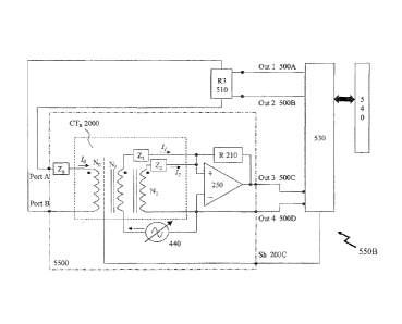
control circuit
530 but is grounded. However, now Out 4 500D, which is coupled to second 4TeR
R2 320, is
coupled with Out 2 500B and therein the control circuit 530 rather than
directly to the control
circuit, Accordingly, variations in the output of the PACCS 5000 which are
applied to the
Load Z 420 under test are automatically applied to the measured current
flowing in the load
circuit via third 4TcR R3 510.
[0046] Within the embodiments of thc invention depicted supra in respect of
precision AC
current sources Figures 3A, 4A and 4B and exploited within the AC shunt
calibrators 550A to
550C in Figures 5A to 5C respectively current sources are employed in
conjunction with the
secondary winding. However, in othcr embodiments of the invention these
current sources
may be an AC power source in order to drive power shunts during calibration.
Such AC
power sources may range from 50W to 1000W, for example.
[0047] Referring to Figures 6 there are depicted first to third dual stage
current transducers
(2SCT1) 600A to 600C respectively designs exploiting core-in-core, dual core,
and triple core
designs respectively to provide AC devices according to embodiments of the
invention as
described in respect of Figures 2 through 5. Referring to first 2SCTR 600A a
magnetic shield,
the first stage magnetic core 610, has wound around it primary winding 620 and
secondary
winding 630. Disposed within the magnetic shield arc electric shield 650 and
correction
winding 640 which surround measuring torpid, second stage magnetic core 660.
[0048] Second 2SCTR 60013 depicts the same elements except that now the first
stage
magnetic core 610 and second stage magnetic core 660 are a pair of parallel
toroids wherein
the primary winding 620 and secondary winding 630 surround both as does the
electrical
shield 650. The correction winding 640 then surrounds only the second stage
magnetic core
660. Similarly in third 2SCTR 600C depicts the same elements except that now
the first stage
- 12-
CA 02885445 2015-03-20
magnetic core comprises first and second core elements 610A and 610B
respectively and
these, in conjunction with the second stage tnagnetic core 660 are a triplet
of parallel toroids.
Accordingly, in third 2SCIR 600C the primary winding 620 and secondary winding
630
surround the first and second core elements 610A and 610B and second stage
magnetic core
660. Thc electrical shield 650 surrounds only the second stage magnetic core
660 as does the
correction winding 640. Other embodiments of a 2SCTR may be envisioned without
departing
from the scope of the invention.
[00491 Figure 7 depicts a dual stage current transducer (2SCTR) design
exploiting a core-in-
core design to provide AC devices according to embodiments of the invention as
described in
respect of Figures 2 through 5 and first 2SCTR 600A. Accordingly first image
700C depicts
the 2SCTR sequentially stripped from the outermost layer towards the centre
whilst second
image 700D depicts a three dimensional quarter-cut sectional view with first
to fifth tape
layers 730A through 730E respectively and shielding 760 removed for clarity.
Accordingly as
shown the 2SCTR comprises a first core comprising first to fourth core
elements 710A to
710D respectively surround a second core 720. Second core 720 then has first
tape layer
730A separating the first winding 740 from it which is then overwound with
second tape
layer 730B. The first core (first to fourth core elements 710A to 710D) and
second core 720
respectively with their respective surrounding layers are then overwound with
third tape layer
730C. Atop third tape layer 730C second winding 750 is wound around first core
(first to
fourth core elements 71 OA to 710D) and second core 720. Second winding 750 is
then
overwound by fourth tape layer 730D, shielding 760, fifth tape layer 730E and
third winding
770.
[0050] As depicted first winding 740 corresponds to correction winding N2 of
Figure 10,
second winding 750 corresponds to secondary winding N1 of Figure 10, and third
winding
770 corresponds to the primary wind Mg No of Figure 10. Optionally a second
shielding may
be disposed between the first and second windings 740 and 750 respectively
such as between
second and third tape layers 730B and 730C respectively. Second image 700D
depicts a three
dimensional quarter-cut sectional view with first to fifth tape layers 730A
through 730E
respectively and shielding 760 removed thereby showing how the first to third
windings 740,
750 and 770 respectively are wound around the closed magnetic elements forming
the first,
second, and third cores 710A, 720, and 710B respectively. It would be evident
to one skilled
in the art that the number of windings for each of the first to third windings
740, 750, and 770
- 13 -
CA 02885445 2015-03-20
respectively and geometries of the first core (first to fourth core elements
710A to 710D) and
second core 720 respectively may be adjusted according to the electrical
voltage, current and
power of the signal being measured and / or generated.
[0051] Figure 8 depicts a dual stage current transducer (2SCTR) design
exploiting a three-
core design to provide AC devices according to embodiments of the invention as
described in
respect of Figures 2 through 5 and third 2SCTR 600C. Accordingly first image
800C depicts
the CT sequentially stripped from the outermost layer towards the centre
whilst second image
SOOD depicts a three dimensional quarter-cut sectional view with first to
fifth tape layers
830A through 830E respectively and shielding 860. Accordingly as shown the CT
comprises
first, second, and third cores 810A, 820, and 810B respectively. Second core
820 then has
first tape layer 830A separating the first winding 840 from it which is then
overwound with
second tape layer 830B. The first, second, and third cores 810A, 820, and 810B
respectively
with their respective surrounding layers are then overwound with third tape
layer 830C. Atop
third tape layer 830C second winding 850 is wound around first, second, and
third cores
810A, 820, and 810B respectively. Second winding 850 is then overwound by
fourth tape
layer 830D, shielding 860, fifth tape layer 830E and third winding 870. As
depicted first
winding 840 corresponds to correction winding N2 of Figure 10, second winding
850
corresponds to secondary winding N1 of Figure 10, and third winding 870
corresponds to the
primary winding No of Figure 10. Optionally a second shielding may be disposed
between the
first and second windings 840 and 850 respectively such as between second and
third tape
layers 830B and 830C respectively.
[0052] Second image 800D depicts a three dimensional quarter-cut sectional
view with first
to fifth tape layers 830A through 830E respectively and shielding 860 removed
thereby
showing how the first to third windings 840, 850 and 870 respectively are
wound around the
closed magnetic elements forming the first, second, and third cores 810A, 820,
and 810B
respectively. It would be evident to one skilled in the art that the number of
windings for each
of the first to third windings 840, 850, and 870 respectively and geometries
of the first,
second, and third cores 810A, 820, and 810B respectively may be adjusted
according to the
electrical voltage, current and power of the signal heing measured and / or
generated.
[0053] Specific details are given in the above description to provide a
thorough
understanding of the embodiments. However, it is understood that the
embodiments rnay be
practiced without these specific details. For example, circuits may be shown
in block
- 14 -
CA 02885445 2015-03-20
diagrams in order not to obscure the embodiments in unnecessary detail. In
other instances,
well-known circuits, processes, algori 'tins, structures, and techniques may
be shown without
unnecessary detail in order to avoid obscuring the embodiments.
[0054] The foregoing disclosure of the exemplary embodiments of the present
invention has
been presented for purposes of illustration and description. It is not
intended to be exhaustive
or to limit the invention to the precise forms disclosed. Many variations and
modifications of
the embodiments described herein will be apparent to one of ordinary skill in
the art in light
of the above disclosure. The scope of the invention is to be defined only by
the claims
appended hereto, and by their equivalents.
[0055] Further, in describing representative embodiments of the present
invention, the
specification may have presented the method and/or process of the present
invention as a
particular sequence of steps. However. to the extent that the method or
process does not rely
on the particular order of steps set forth herein, the method or process
should not be limited to
the particular sequence of steps described. As one of ordinary skill in the
art would
appreciate, other sequences of steps may be possible. Therefore, the
particular order of the
steps set forth in the specification should not be construed as limitations on
the claims. In
addition, the claims directed to the method and/or process of the present
invention should not
be limited to the performance of their steps in the order written, and one
skilled in the art can
readily appreciate that the sequences may be varied and still remain within
the spirit and
scope of the present invention.
- 15 -