Note: Descriptions are shown in the official language in which they were submitted.
CA 02886374 2015-03-26
WO 2014/055292 PCMJS2013/061428
PROCESSOR-BASED CIRCUIT INTERRUPTING DEVICES
BACKGROUND
Technical Field
The present disclosure relates generally to processor-based circuit
interrupting
devices. In particular, the present disclosure relates to microcontroller-
based circuit
interrupting devices having noise protection and/or self-test functions.
Description of Related Art
Many electrical wiring devices have a line side, which is connectable to an
electrical power supply, and a load side, which is connectable to one or more
loads and at
least one conductive path between the line and load sides. Electrical
connections to wires
supplying electrical power or wires conducting electricity to the one or more
loads are at line
side and load side connections. Presently available ground fault circuit
interrupting (GFCI)
devices, such as the device described in commonly owned U.S. Pat. No.
4,595,894, use an
electrically activated trip mechanism to mechanically break an electrical
connection between
the line side and the load side. Such devices are resettable after they are
tripped by, for
example, the detection of a ground fault. In the device discussed in the '894
patent, the trip
mechanism used to cause the mechanical breaking of the circuit (i.e., the
conductive path
between the line and load sides) includes a solenoid (or trip coil). A test
button is used to test
the trip mechanism and circuitry used to sense faults, and a reset button is
used to reset the
electrical connection between line and load
sides.
However, instances may arise where an abnormal condition, caused by for
example a lightning strike, occurs which may result not only in a surge of
electricity at the
device and a tripping of the device but also a disabling of the trip mechanism
used to cause
the mechanical breaking of the circuit. Further, an open neutral condition,
which is defined in
Underwriters Laboratories (UL) Standard PAG 943A, may exist with the
electrical wires
supplying electrical power to such GFCI devices. Commonly owned application
Ser. No.
09/138,955 filed Aug. 24, 1998 (now U.S. Pat. No. 6,040,967),
describes a family of resettable circuit interrupting devices
capable of locking out the reset portion of the device if the circuit
interrupting portion is non-
operational or if an open neutral condition exists.
Some of the circuit interrupting devices described above have a user
accessible
load side connection in addition to the line and load side connections. The
user
accessible load side connection includes one or more connection points where a
user can
externally connect to electrical power supplied from the line side. The load
side connection and
user accessible load side connection are typically electrically connected
together. An example of
such a circuit interrupting device is a GFCI receptacle, where the line and
load side connections
are binding screws and the user accessible load side connection is the plug
connection to an internal receptacle. As noted, such devices are connected to
external wiring
so that line wires are connected to the line side connection and load side
wires are connected to
the load side connection. However, instances may occur where the circuit
interrupting device is
improperly connected to the external wires so that the load wires are
connected to the line side
connection and the line wires are connected to the load connection. This is
known as reverse wiring. In the event the circuit interrupting device is
reverse wired, fault
protection to the user accessible load connection may be eliminated, even if
fault protection
to the load side connection
remains.
Commonly owned application Ser. No. 13/192,860 filed July 28, 2011 (now
2
Date Recue/Date Received 2021-06-10
U.S. Pat. No. 8,130,480), describes a family of resettable circuit
interrupting devices capable of
locking out the reset portion of the device if the circuit interrupting
portion is non-operational or if
an open neutral condition exists, and also capable of providing reverse wiring
protection.
Other circuit interrupting devices include arc fault circuit interrupting
devices
(AFCI's), immersion detection circuit interrupting devices (IDCI's), appliance
leakage circuit
interrupting devices (ALCI's), equipment leakage circuit interrupting devices
(ELCI's), circuit
breakers, contactors, latching relays and solenoid mechanisms.
SUMMARY
The present disclosure is directed to processor-based circuit interrupting
devices. In one aspect of the present disclosure, a fault circuit interrupting
device includes a fault
sensor configured to output a sensor signal; a voltage sensor configured to
sense a reference
voltage; and a controller configured to determine an occurrence of an actual
fault based on the
sensor signal and the reference voltage. The fault circuit interrupting device
further includes an amplifier configured to receive the sensor signal and the
reference voltage
and output an amplified signal. The fault circuit interrupting device further
includes an analog-
to-digital converter configured to receive the reference voltage and the
amplified signal and
output respective digital signals corresponding to the reference voltage and
the amplified signal.
The fault circuit interrupting device further includes a line interrupt
assembly. The line interrupt assembly interrupts current flow through a
conductive path
when the characteristic of the sensor signal exceeds an actual fault
threshold. The fault sensor can
be a differential transformer.
3
Date Recue/Date Received 2021-06-10
CA 02886374 2015-03-26
WO 2014/055292 PCT/US2013/061428
The processor is selected from the group consisting of a microcontroller, a
system on chip (SOC), and a field programmable gate array. The processor is
further
configured to determine whether the reference voltage exceeds a voltage
threshold in
determining the occurrence of the actual fault.
The amplifier amplifies a characteristic of the sensor signal in accordance
with
a gain. The amplified signal has a frequency identical to a frequency of the
sensor signal.
The fault circuit interrupting device further includes a gain circuit,
wherein,
based on the frequency of the sensor signal, the gain circuit adjusts the gain
accordingly. The
gain is adjusted to a first adjusted gain when the sensor signal has a first
frequency, and the
gain is adjusted to a second adjusted gain when the sensor signal has a second
frequency.
The fault circuit interrupting device further includes a self-test circuit
configured to automatically initiate a self-test. The self-test includes
circuitry configured to
generate a simulated fault for testing operation of the fault circuit
interrupting device.
The fault circuit interrupting device further includes a manual test assembly
comprising a test button configured to initiate a test. The test is configured
to interrupt a
conductive path and generate a simulated fault.
The fault circuit interrupting device further includes an arc fault sensor
configured to output an arc sensor signal, indicative of an arc fault
condition, to the
controller. The controller is configured to trigger a line interrupt assembly
when the arc
sensor signal exceeds an arc fault threshold.
The fault circuit interrupting device further includes a resistor connected
across a first and a second conductor via which the sensor signal is output
from the fault
4
CA 02886374 2015-03-26
WO 2014/055292 PCT/US2013/061428
sensor for avoiding saturation of the fault sensor. The fault sensor includes
a differential
transformer.
The fault circuit interrupting device further includes a grounded neutral
transformer configured to output a signal if a neutral conductor is grounded.
The fault circuit interrupting device further includes a test circuit
configured to
generate a simulated electrical fault condition. The controller is further
configured to initiate
a test operation including triggering the test circuit to generate the
simulated fault condition,
determine whether a characteristic of the amplified signal exceeds a test
fault threshold
during performance of the test operation without triggering a line interrupt
assembly unless a
characteristic of the amplified signal exceeds an actual fault threshold, and
indicate the
occurrence of a test failure when the test operation terminates and the
determination is false.
The line interrupt assembly interrupts current flow through a conductive path
when the
characteristic of the amplified signal exceeds the actual fault threshold.
The fault circuit interrupting device further includes a memory unit. The
controller is configured to execute an algorithm for calculating a gain of the
amplifier. The
algorithm including at least one constant that influences the determination of
the gain, the at
least one constant being stored in the memory unit, and the controller is
further configured to
adjust the at least one constant for adjusting the calculation of the gain
during a calibration
procedure.
The controller is further configured to determine an expected value for a
characteristic of the amplified signal during a test operation in which the
value of a
characteristic of the at least one signal is known, determine the value for
the characteristic of
the amplified signal as measured during the test operation, determine a
difference between
5
CA 02886374 2015-03-26
WO 2014/055292 PCT/US2013/061428
the expected value for the characteristic of the amplified signal and the
determined value for
the characteristic of the amplified signal, store the difference as an offset
compensation
constant in the memory unit, and apply the offset compensation constant in
subsequent
determinations of the value of the characteristic of the amplified signal.
The controller includes a compensation module for determining when the
amplifier is saturated and, based on determining the amplifier is saturated,
adjusts a value of a
characteristic of the amplified signal by a predetermined factor.
The controller is further configured to iteratively sample a characteristic of
the
amplified signal, and calculate an integrated value for the characteristic of
the amplified
signal iteratively, including executing an integration algorithm using the
sampled values for
the characteristic of the amplified signal.
The fault circuit interrupting device further includes a voltage regulator
having
a linear regulator component. The controller is further configured to control
the linear
regulator component. The linear regulator component includes a variable
resistor and the
controller controls the resistance of the variable resistor.
The controller is further configured to monitor a voltage input to a voltage
regulator for detecting when a bridge diode fails to conduct current.
The controller is further configured to perform at least one diagnostic test
to
check at least one component of the fault circuit interrupting device.
The fault circuit interrupting device further includes at least one sensor
configured to sense an environmental parameter and provide an output signal
indicative of
the environmental parameter. The controller is further configured to adjust at
least one
software component of the fault circuit interrupting device in accordance with
the output
6
CA 02886374 2015-03-26
WO 2014/055292 PCT/US2013/061428
signal indicative of the environmental parameter. The environmental parameter
is humidity
and/or temperature. The sensor is located internally within the fault circuit
interrupting
device, located externally of the fault circuit interrupting device, and/or
integrated with the
controller.
The controller is further configured to interrupt current flow to a conductor
if
the occurrence of an actual fault is determined. The controller is further
configured to
determine an RMS value of the sensor signal.
The controller is selected from the group consisting of a microcontroller,
system on chip (SOC), and field programmable gate array (FPGA). The circuit
interrupting
device is selected from the group consisting of a GFCI device, an AFCI device,
and a
GFCl/AFCI device.
According to another aspect of the present disclosure, there is provided a
fault
circuit interrupting device which includes a fault circuit interrupting
circuit for interrupting
current flow through a conductive path after detection of a fault condition; a
voltage regulator
in operative communication with the fault interrupting circuit and configured
to receive a
voltage; and a controller configured to monitor the voltage for detecting
failure of a diode of
a bridge rectifier. The fault circuit interrupting device is selected from the
group consisting
of a GFCI device, an AFCI device, and a GFCl/AFCI device.
According to another aspect of the present disclosure, there is provided a
fault
circuit interrupting device which includes a first sensor configured to output
a first signal
having a first frequency and a first characteristic; a second sensor
positioned in proximity to
the first device; a gain circuit including a frequency dependent component
configured to
adjust a gain based on the frequency of the first signal such that when the
first signal has a
7
CA 02886374 2015-03-26
WO 2014/055292 PCT/US2013/061428
first frequency, the gain is adjusted to a first adjusted gain, and when the
first signal has a
second frequency, the gain is adjusted to a second adjusted gain that is
different than the first
adjusted gain; an amplifier configured to receive the first signal and amplify
the first
characteristic in accordance with either the first or second adjusted gain,
and outputting a
corresponding amplified signal having a second characteristic and the same
frequency as the
first signal; a line interrupt assembly configured to interrupt flow of
current through a
conductor when triggered; and a controller configured to trigger the line
interrupt assembly
when the second characteristic exceeds an actual fault threshold.
The fault circuit interrupting device further includes an arc fault circuit
interrupter (AFCI) circuit that outputs an arc signal indicative of an arc
fault condition to the
controller, wherein the controller is configured to trigger the line interrupt
assembly when the
arc signal provided by the AFCI circuit exceeds an arc fault threshold. The
first sensor is a
differential transformer, the electrical fault is a ground fault, and the
second sensor is a
grounded neutral transformer.
The fault circuit interrupting device further includes a reference voltage
circuit
configured to receive a voltage signal from a power source and output a
corresponding
reference signal having a reference voltage. The amplifier is configured to
further receive the
reference signal; and the controller is further configured to receive a
digitized value
corresponding to the reference voltage and trigger the line interrupt assembly
when the
second characteristic of the amplified signal exceeds the actual fault
threshold and the
received voltage value for the reference voltage does not exceed a noise
threshold.
The fault circuit interrupting device further includes a self-test assembly
configured to automatically initiate a self-test. The self-test includes
generating a simulated
8
CA 02886374 2015-03-26
WO 2014/055292 PCT/US2013/061428
fault for testing operation of said system. The fault circuit interrupting
device further
includes a manual test assembly having a test button configured to initiate a
test. The test
includes opening at least one contact in electrical communication with the
conductor and
generating a simulated fault.
According to another aspect of the present disclosure, there is provided a
method for monitoring a circuit for an electrical fault condition. The method
includes
receiving a voltage signal and generating a reference voltage signal;
digitizing the reference
voltage signal using an analog-to-digital converter and generating a digital
signal
corresponding to the reference voltage signal; and processing the digital
signal corresponding
to the reference voltage signal and a sensor signal outputted from a
transformer for
determining the occurrence of an electrical fault condition. The method
further includes
interrupting delivery of current to a load if occurrence of the electrical
fault condition is
determined.
According to another aspect of the present disclosure, there is provided a
circuit interrupting device which includes a sensing device in operative
communication with
a solenoid. The sensing device is configured for sensing an electrical fault
condition and
generating a signal in response to the sensed electrical fault condition for
moving the
solenoid. The electrical fault condition is associated with current flowing
through a
conductor electrically coupled to a power source which generates a current
output. The
sensing device further includes an amplifier configured for receiving the
signal and
generating an amplified signal; a test circuit configured to generate a
simulated fault
condition along the conductor; a line interrupt assembly configured to
interrupt current flow
through the conductor; and a controller configured to control the test circuit
for initiating a
9
CA 02886374 2015-03-26
WO 2014/055292 PCT/US2013/061428
test operation which includes triggering the test circuit to generate the
simulated fault
condition.
The test operation terminates after a predetermined time interval. The
predetermined time interval is less than a time required to trigger the line
interrupt assembly
after occurrence of an actual fault. The simulated fault condition includes a
test signal. An
amplitude of the test signal is less than an amplitude of the signal during an
actual fault.
The conductor can be a first conductor, and the system includes a second
conductor. The simulated fault condition includes generating an imbalance in
currents
passing through the first and second conductors. The imbalance includes adding
a
supplemental current to at least one of the first and second conductors. The
supplemental
current is not synchronized with the current output by the power source. The
supplemental
current is generated through a substantial portion of two half cycles
associated with the
current output by the power source. The two half cycles are successive half
cycles.
Other features of the presently disclosed circuit interrupting devices will
become apparent from the following detailed description, taken in conjunction
with the
accompanying drawings, which illustrate, by way of example, the presently
disclosed circuit
interrupting devices.
BRIEF DESCRIPTION OF THE DRAWINGS
Various embodiments of the present disclosure will be described below with
reference to the figures, wherein:
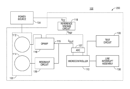
FIG. 1 is a block diagram of an exemplary ground fault circuit interrupting
(GFCI) system in accordance with the present disclosure;
CA 02886374 2015-03-26
WO 2014/055292 PCT/US2013/061428
FIG. 2 is a block diagram of an exemplary embodiment of the GFCI system
shown in FIG. 1;
FIG. 3 is a circuit diagram of an operational amplifier and an associated gain
circuit of the embodiment of the GFCI system shown in FIG. 2;
FIGs. 4A and 4B illustrate a schematic circuit diagram of the GFCI system
shown in FIG. 2;
FIG. 5 is a block diagram of a microcontroller of the embodiment of the GFCI
system shown in FIG. 2; and
FIG. 6 is a block diagram of an exemplary GFCI and arc fault circuit
interrupting (AFCI) system in accordance with the present disclosure.
DETAILED DESCRIPTION
A ground fault circuit interrupting (GFCI) system, which may include a
ground fault circuit interrupting (GFCI) device, or a GFCI device combined
with an arc fault
circuit interrupting (AFCI) device, is taught. The GFCI system includes a GFCI
device or a
GFCl/AFCI device having a processor coupled to one or more transformers that
detect one or
more electrical fault conditions. The processor can be a microcontroller (FIG.
1), a system on
chip (SOC) (FIG. 2), field programmable gate array (FPGA), etc. Collectively
the one or
more components, which can include the processor, microcontroller, SOC, and/or
FPGA, for
performing the various functions and operations described herein are part of a
controller, as
recited, for example, in the claims.
The processor, microcontroller, etc. processes signals output by the
transformers and determines when an electrical fault condition has occurred.
In one
11
CA 02886374 2015-03-26
WO 2014/055292 PCT/US2013/061428
embodiment, for example, the microcontroller is provided as a single
integrated circuit (IC)
chip which can be mounted on a single printed circuit board (PCB).
Alternatively, the
various circuit components, including, for example, the processor,
microcontroller, etc. are
provided as one or more integrated circuit chips. That is, the various circuit
components are
located on one or more integrated circuit chips.
The GFCI device includes a reference voltage circuit that receives and
processes a power signal and generates a corresponding reference voltage
signal. The GFCI
device uses an operational amplifier (opamp) to amplify a sensor signal, e.g.,
a voltage
differential signal generated by a differential transformer indicative of the
occurrence of a
first electrical fault condition. The reference voltage signal is input to
both the opamp and
the microcontroller. The microcontroller executes software that processes the
reference
voltage signal and the amplified voltage differential signal, ignoring high
amplified
differentials that would otherwise indicate the occurrence of a fault
condition when a value
(e.g., magnitude) of the reference voltage signal exceeds a noise threshold Tõ
(e.g., a voltage
threshold) The effect is to improve noise immunity by filtering out high
energy spurious
noise that is not related to a ground fault, grounded neutral fault, or arc
fault condition.
Additionally, the GFCI device is provided with a frequency dependent gain
circuit that applies a first gain when amplifying a voltage differential
indicative of detection
of a ground fault signal, and a second gain when amplifying a voltage
differential indicative
of detection of a grounded neutral fault signal.
The microcontroller executes a variety of software modules, including an
integrator module that integrates the amplified differential signal while
subtracting a value
(e.g., a bleed value), thereby summing the amplified differential signal
without accumulating
12
CA 02886374 2015-03-26
WO 2014/055292 PCT/US2013/061428
unwanted noise; a gain determination module for adjusting gain constants for
calibrating the
GFCI device; an opamp offset compensation module for determining and
compensating for
voltage offset of the opamp; and an opamp saturation compensation module for
recognizing
and compensating for opamp saturation.
Additionally, the microcontroller executes one or more software modules to
automatically initiate a self-test, including triggering the creation of a
simulated fault, in
response to an event or a predetermined schedule and initiates a manual test
in response to
manual activation of a test actuator. Furthermore, the microcontroller
executes one or more
software modules to recognize when an actual fault or a simulated fault was
sensed, including
distinguishing between the occurrence of an actual fault and the occurrence of
a simulated
fault, triggers circuit interruption when an actual fault has been recognized,
and indicates
when a self-test or a manual test has failed.
During a self-test, the fault level may have a lower magnitude than the fault
level required to be detected/interrupted during actual operation.
Furthermore, during a self-
test, fault detection may occur in a shorter time period than the minimum time
requirement
for recognition and interruption of a fault during actual operation. This
avoids interference
with circuit interruption and allows for a timely response in the event of an
actual fault
occurring simultaneously during a self-test. The self-test of the GFCI device
according to the
present disclosure can be performed at lower current levels (e.g., 4 ma or
below), without
tripping the GFCI device, as opposed to a manual test (e.g., 8 ma or below).
During the self-
test, the GFCI device can detect the occurrence of an actual fault which
warrants circuit
interruption, as opposed to prior art GFCI devices which cannot detect the
occurrence of an
actual fault during testing.
13
CA 02886374 2015-03-26
WO 2014/055292 PCT/US2013/061428
Referring now to the figures, in which like reference numerals identify
identical or corresponding elements, the GFCI system in accordance with the
present
disclosure will now be described in detail. With initial reference to FIGS. 1,
2, and 4, an
exemplary GFCI system in accordance with the present disclosure is illustrated
and is
designated generally GFCI system 100. GFCI system 100 includes a GFCI device
200
having a fault sensor assembly 102 that senses a variety of electrical faults
associated with
phase and neutral line signals provided by a power source 104 (e.g., 120 VAC),
such as for
delivery to a load 106 (see FIG. 2). The power signal provided by the power
source 104, may
be, for example, a power signal provided by a utility company, or a power
signal provided to
a portion of a residential or commercial electrical system, such as via a
branch circuit.
Output from the fault sensor assembly 102 is provided to a microcontroller
110 which controls a line interrupt assembly 108 that is configured to
interrupt power to the
load 106 upon detection of a fault condition. In some instances, the load 106
may be an
unintended load, such as a person receiving a shock, and the interruption of
power prevents
current from flowing through the person. Additionally, microcontroller 110
controls a test
circuit 109 that is configured to initiate a test fault condition.
The fault sensor assembly 102 includes a differential current transformer
(e.g.,
a fault sensor) 112 and a grounded neutral (GIN) transformer 114. The
differential
transformer 112 detects or senses an imbalance between current flowing through
the phase
and neutral conductors which is indicative of a ground fault condition. When
an imbalance is
detected, the differential transformer 112 outputs a differential signal
having a voltage (herein
referred to as a differential voltage) that corresponds to the sensed
difference between the
currents flowing through the phase and neutral conductors. A first part of the
differential
14
CA 02886374 2015-03-26
WO 2014/055292 PCT/US2013/061428
signal Si is provided to a negative input terminal 111 of an operational
amplifier (opamp)
116, and a second part of the differential signal S2 is provided to a positive
input terminal
113 of the opamp 116 that amplifies the differential voltage in accordance
with the gain of
the opamp 116 and outputs a corresponding signal Sour from an output terminal
115 of
opamp 116 having a voltage Vout that corresponds to amplification of the
differential
voltage. When a ground fault condition occurs, the differential signal has a
first frequency fl
that corresponds to the frequency fl of the signals flowing through the phase
and neutral
conductors, e.g., the power signal frequency.
A reference voltage signal Sref having a voltage Vref is generated by a
reference voltage circuit 118 and provided to the positive terminal 113 of the
opamp 116 as
well as to the microcontroller 110. The reference voltage circuit 118 receives
an input
voltage signal having voltage Vcc from the power source 104 and includes one
or more
electrical components, such as a resistor divider circuit, for operating the
input voltage signal
in a predetermined fashion for generating Vref as function of Vcc. The
reference voltage
.. circuit 118 reduces Vcc in accordance with a predetermined factor and
outputs reference
signal Sref having voltage Vref. In the present example, Vref = V2(Vcc),
however other
predetermined functions are envisioned, provided that 0 < Vref < Vcc.
The predetermined function is provided to microcontroller 110 such that the
microcontroller 110 recognizes an acceptable range for Vref and can
extrapolate information
about Vcc based on Vref. By providing Sref to both the input of the opamp 116
and the
microcontroller 110, the microcontroller 110 can determine quickly in real-
time when Vref
exceeds a noise threshold Tn. If Vref exceeds the noise threshold it indicates
that a high value
output from the output terminal 115 of opamp 116 is not due to an actual fault
(i.e., a fault
CA 02886374 2015-03-26
WO 2014/055292 PCT/US2013/061428
warranting circuit interruption) but to spurious noise generated by the power
source 104 that
does not warrant circuit interruption. That is, the high value output is not
due to an actual
fault condition (e.g., arcing, high current flow, etc.) that should trigger a
circuit interruption.
Spurious noise may be caused, for example, by a power surge, switching power
supplies, fans
controlled by switches and fan controllers, chattering relays, and high energy
pulses.
Noise immunity is improved by providing Sref to microcontroller 110 for
filtering out spurious noise. This allows for elimination of conventional
analog filter
components configured to filter out spurious noise, such as a large
capacitance capacitor
(>1uF) in the power source 104 or voltage regulator 150 (see below). By
eliminating the use
of such a large capacitance capacitor, power-up can be faster and without
transition to a
charged state, cost is reduced, and consumption of space on the PCB is
reduced.
Additionally, the microcontroller 110 can monitor noise on the power source
104 using
another reference voltage and/or other solutions that are known in the art
voltage monitoring.
Opamp 116 may be integrated with microcontroller 110 or distinct therefrom.
An analog-to-digital converter (ADC) 127 is provided that may be a standalone
device (see
FIG. 2) or may be integrated with opamp 116 and/or microcontroller 110 (see
FIG. 4A).
When Vout exceeds an actual fault threshold Taf and Sref does not exceed the
noise threshold Tõ, then the microcontroller 110 treats the occurrence as an
indication of an
actual fault, as opposed to noise. The microcontroller 110 may further process
Vout, such as
by performing an integration algorithm, for determining if an actual fault has
occurred.
When the processing results indicate that an actual fault has occurred,
microcontroller 110
triggers a circuit interruption.
16
CA 02886374 2015-03-26
WO 2014/055292 PCT/US2013/061428
However, when the microcontroller 110 determines that Vout exceeds the
fault threshold Taf and Vref exceeds the noise threshold Tõ based on
acceptable values for
Vcc and the predetermined function, then there is not an indication that an
actual fault has
occurred. Vout is ignored and is not further processed for determining if an
actual fault has
occurred. This improves noise immunity by avoiding unnecessary circuit
interruption.
The grounded neutral transformer 114 and the differential transformer 112 are
arranged or configured to be in a proper electrical phase relationship with
respect to each
other. This may be achieved in any suitable manner, such as, for example,
physically
positioning or arranging the grounded neutral transformer 114 and the
differential
transformer 112 in a particular orientation with respect to each other such
that the direction of
current flow in one transformer is along a particular direction with respect
to the direction of
current flow of the other transformer. The resonant circuit 120 may include a
capacitor
having a selected capacitive value that will create resonance upon inductance
of the grounded
neutral transformer 114.
Output of the opamp 116 at output terminal 115 is connected through the
resonant circuit 120 to the grounded neutral transformer 114. The opamp 116 is
in a proper
electrical phase relationship with the differential transformer 112 such that
opamp 116
oscillates upon the occurrence of a grounded neutral condition at a second
frequency f2, such
as when an unwanted electrical path is created between the phase conductor and
a ground
conductor. When a grounded neutral condition is present, the grounded neutral
transformer
114 injects or outputs a signal into the line. The signal creates an imbalance
in the currents
passing through differential transformer 112 which causes the differential
transformer 112 to
17
CA 02886374 2015-03-26
WO 2014/055292 PCT/US2013/061428
output the differential signal having the second frequency f2. In the present
example, 12 = 6-
7 kHz.
With continued reference to FIGS. 2 and 3, an exemplary embodiment of
GFCI system 100 is shown in greater detail, including gain circuit 124 that is
configured to
determine a gain G for opamp 116 that defines the degree of amplification
provided by
opamp 116. Gain circuit 124, including first and second gain circuits 124a and
12b, one or
more resistors, and a frequency dependent component 126. Examples of the
frequency
dependent component 126 include a differentiating capacitor or a filtering
circuit, e.g., a
bandpass filter. Whereas the gain circuit 124 determines the gain G for opamp
116, the
frequency dependent component 126 varies the gain G of opamp 116 based on the
frequency
of current passing through frequency dependent component 126.
When a ground fault occurs, differential transformer 112 is induced to
generate a differential signal (e.g., signals S1 and S2) having a differential
voltage and
frequency fl , which is substantially equal to the frequency of the phase and
neutral signals
provided by the power source 104, e.g., 60Hz. The differential voltage, e.g.,
VI-V2, is
amplified by opamp 116 using a gain sufficient to detect faults ranging
between 4ma and
6ma, e.g., by setting G substantially equal to M.
When a grounded neutral fault occurs, since grounded neutral transformer 114
is in a proper electrical phase relationship with the differential transformer
112, differential
transformer 112 generates a differential signal having frequency 12 that
corresponds to the
resonance frequency of resonant circuit 120, e.g., 6-7 kHz. A substantially
higher gain G is
needed to provide oscillation during a grounded neutral condition, e.g., when
the differential
signal has a frequency of 12. Accordingly, when the differential signal has a
frequency 12, G
18
CA 02886374 2015-03-26
WO 2014/055292 PCT/US2013/061428
is set to N, where N is substantially greater than M. Frequency dependent
component 126 is
configured to achieve the higher gain G when the frequency of the differential
signal is 12.
Phase and neutral line signal inputs are provided to conductors 101, 103,
respectively, at a line side 117 thereof, and delivered at a load side 119
thereof to a load 106.
Load 106 may be an intended load, such as an appliance or circuit, or an
unintended load.
The differential transformer 112 in the current example has a toroidal core
105 formed of a
very high permeability material, such as permalloy (a nickel-iron magnetic
alloy, with about
20% iron and 80% nickel content). The phase and neutral conductors 101 and 103
pass
through the core 105 as primary windings. The differential transformer 112 is
provided with
a secondary winding 130 having a first end 131 and a second end 133. When
there is an
imbalance between currents flowing through the phase and neutral conductors
101 and 103
indicative of a ground fault condition, a current is induced in the secondary
winding 130. A
ground fault condition may be caused, for example, when an unwanted electrical
path is
created between the phase conductor 101 and a ground conductor.
The first and second ends 131 and 133 arc coupled to an analog to digital
converter (ADC) 127. In the present example, the ADC 127 is integrated with
the opamp 116
which is integrated with the microcontroller 110, such as, for example, to
provide a system on
chip (SOC). In other embodiments one or more of the components ADC 127, the
opamp
116, and the microcontroller 110 may be discrete from the other component(s).
Alternatively, analog-to-digital conversion may be performed to the signal
output by opamp
116 after amplification by opamp 116. The ADC 127 further receives Vref and
converts it to
a digital signal.
19
CA 02886374 2015-03-26
WO 2014/055292 PCT/US2013/061428
Sref is coupled to first end 131, which is further coupled to the positive
input
terminal 113 of opamp 116. Thus the voltage Vref is summed with V2 or biases
V2. Opamp
116 amplifies VI + Vref ¨ V2 and outputs Sour having voltage Vout. Thus, when
Vref
spikes due to a spike in Vcc, Vout may spike as well. Since digitized Vref is
further input to
microcontroller 110, microcontroller 110 applies the predetermined function
and an expected
range of values for Vcc to determine whether Vref exceeds a noise threshold T.
If so, an
occurrence of Vout > Tõ may be caused by a power source related event rather
than a ground
fault event.
A burden resistor 138 having a resistor value of about at least lkohm is
provided across ends 131, 133 to prevent magnetizing of the differential
transformer 112 and
to prevent saturation of the differential transformer 112 when detecting a
fault associated
with high current. The burden resistor ensures current flow across ends 131,
133 providing
counter flux to counteract the buildup of flux due to a high current,
minimizing the
occurrence of saturation of the core.
The grounded neutral transformer 114 in the current example has a toroidal
core 107 formed of a magnetic material, such as ferrite. The grounded neutral
transformer
114 operates together with the differential transformer 112 to create feedback
for the
amplifier 116 when a grounded neutral fault condition exists. The phase and
neutral
conductors 101 and 103 further pass through the core 107 as primary windings.
The
grounded neutral transformer 114 is provided with a secondary winding 134
having a first
end 135 and a second end 137.
Resonant circuit 120 is coupled to first and second ends 135, 137, with second
end 137 terminating in a ground connection. First end 135 is further coupled
to the negative
CA 02886374 2015-03-26
WO 2014/055292 PCT/US2013/061428
input terminal 111 of the opamp 116. Resonant circuit 120 is further coupled
via gain circuit
124b to the output from terminal 115 of opamp 116. When a grounded neutral
fault occurs,
resonant circuit 120 oscillates at its resonant frequency f2, inducing a
current in the neutral
conductor 103 which is detected as a ground fault by the differential
transformer 112. When
no such grounded neutral fault is detected, the resonant circuit 120 acts
simply as a load and
does not affect operation of the differential transformer 112.
Regulations specify the time interval in which a circuit interruption must
take
place upon the occurrence of a fault condition. The greater the magnitudes of
the fault
condition, the faster regulations expect circuit interruption to take place.
For example,
timing requirements specify that upon occurrence of a ground fault > 250mA,
the GFCI
device 200 must interrupt the circuit in less than about 24 ms or about 3 half
cycles. This can
be particularly difficult to achieve during a power-up stage in which the
power-up process
can slow down interruption of the circuit. In order to accelerate the power-up
process, power
source 104 is provided with a voltage regulator 150 which includes a linear
regulator
.. component 152. The voltage regulator 150 can also be an integrated circuit
chip, or have a
discrete MOSFET or other controllable semiconductor component located
externally.
GFCI device 200 may further include one or more sensors 160 that sense
environmental conditions or parameters, such as temperature or humidity, and
provide an
output signal to microcontroller 110 indicative of the sensed environmental
conditions. The
environmental conditions may affect the sensitivity of the physical components
of GFCI
device 200, including differential transformer 112 and/or the grounded neutral
transformer
114. Accordingly, the output from sensors 160 can be used by microcontroller
110 to make
21
CA 02886374 2015-03-26
WO 2014/055292 PCT/US2013/061428
adjustments to one or more components, including software components, for
achieving the
sensitivity and precision required for sensing fault conditions.
For example, outside the temperature range of -35 degrees Celsius to 66
degrees Celsius the magnetic property of the differential transformer 112 can
change and
affect the performance of the GFCI device 200. A temperature sensor 160 can
sense the
temperature and determine if it is not within this range. If the temperature
is not within this
range, the sensor 160 transmits a signal to the microcontroller 110 to
compensate for the
change in the magnetic property of the differential transformer 112 by
adjusting, for example,
the value of C[i] in equation (3). Sensors 160 may be provided on an external
face of the
GFCI device 200, provided internal to the GFCI device 200, or be part of or
incorporated
with the microcontroller 110.
GFCI device 200 further includes a manual test button 170 that may be
manually activated by a user for initiating a test routine using test circuit
109. Test button
170 may be provided on an external face of the GFCI device 200. As described
further
below, a test routine may be activated by microcontroller 110 without manual
activation of
test button 170. Manual activation of test button 170 opens contacts 173
(which may be
provided as along lines identified by P_POSTSORE and N_POST_CORE), effectively
tripping the GFCI device 200, thus eliminating the possibility of sensing the
occurrence of an
actual fault during a manually activated test routine.
With reference to FIG. 3, the gain circuits 124a and 124b and inputs to opamp
116 are shown in greater detail. Si and Sref are input to positive input
terminal 113, and S2
is input to the negative input terminal 111. Gain circuit 124a influences
inputs 51 and S2.
Frequency dependent component 126 influences S2, affecting the gain G in
accordance with
22
CA 02886374 2015-03-26
WO 2014/055292 PCT/US2013/061428
the frequency of S2. Gain circuit 124b operates on the SouTas feedback to
negative input
terminal 111.
With reference to FIG. 5, the microcontroller 110 is shown in greater detail.
The microcontroller 110 includes a central processing unit (CPU) 502; at least
one memory
unit 504, which may include one more types of memory, such as RAM, ROM, flash
memory,
EEPROM, etc.; a plurality of input/output ports 506; a clock unit CLK 508;
opamp 116;
ADC 127; and software modules 520 which include a series of programmable
instructions
that are executable by the CPU 502. The series of programmable instructions
can be stored on
a computer-readable medium accessible by the CPU 502, such as memory unit 504,
for
performing the functions disclosed herein and to achieve a technical effect in
accordance with
the disclosure.
The software modules 520 include several modules that may be discrete from
one another or integrated together. The modules include a sampler module 522,
an integrator
module 524, a gain determination module 526, a test routine control module
528, an opamp
offset compensation module 530, an opamp saturation compensation module 532, a
reference
voltage Vref correction module 534, an RMS determination module 536, and a
fault
determination module 538.
The sampler module 522 consults CLK 508 and controls sampling measured
values, such as Vref and Vout output from the output terminal 115 of the opamp
116. In the
current example, the sampling module 522 controls sampling to occur
approximately every
255 us, or approximately 32 times per 60 Hz half cycle.
The gain determination module 526 receives a digitized form of Vout output
from the output terminal 115 of opamp 116 and performs a gain calculation in
software by
23
CA 02886374 2015-03-26
WO 2014/055292 PCT/US2013/061428
applying one or more equations that use one or more gain constants. The gain
determination
module 526 is calibrated by adjusting the one or more gain constants for the
calculation to
achieve the requisite sensitivity, as per requirements set by regulations,
e.g., UL Standards,
to sense ground faults within a predetermined range, which in the present
example is 4-6 mA.
The required sensitivity is achieved by selection of resistor components in
the gain circuit
124 (see FIG. 2) and selection of the software gain constants, for example,
selection of C[i] in
Equation (3) below. The software gain constants (e.g., C[i]) are stored in
memory unit 524,
e.g., in flash memory or EEPROM.
Accordingly, by combining software calculations with the use of analog
components in the gain circuit 124, adjustments for achieving the required
sensitivity may be
made to the software gain constants without adjusting any hardware components.
The
calibration of the software gain constants may be performed at predetermined
intervals or in
response to an event, by performing an automatic diagnostic routine.
Additionally, the output from sensors 160 may be used to adjust the gain
constants. A change in the output from sensors 160 may trigger a recalculation
of the gain
constants and/or performance of an automatic diagnostic routine.
Test routine control module 528 may initiate a test routine or be activated by
an external event, such as activation of test button 170. When a test routine
is initiated by
manual activation of test button 170, the opamp offset compensation module 526
may be
activated. Operational amplifiers typically have an associated input offset
voltage which is
amplified along with the input signal, causing an error that is significant in
the GFCI device
200 because of the small differential voltage that is being amplified. Input
offset voltage may
further be influenced by ambient temperature. The opamp offset compensation
module 530
24
CA 02886374 2015-03-26
WO 2014/055292 PCT/US2013/061428
compensates for the input offset voltage by measuring the differential voltage
during a test
routine that was initiated by activation of test button 170 which opens
contacts 172 and
excludes the possibility of an actual fault condition. During a manual test
the expected value
for Vout is known. The actual value for Vout is measured. The difference
between the
expected value for Vout and the actual value for Vout is determined and used
as a
compensation constant Ccomp that is subtracted in subsequent calculations from
measured
values associated with Vout.
Integrator module 524 performs an integration algorithm. Equations (1) - (3)
below illustrate an exemplary algorithm for determining when a fault has
occurred:
Vout[i+1] = Vout[i] ¨ Bleed[i]; if Vout[i] > Bleed[i]; Equation (1)
Vout[i+1] = 0 if Vout[i] <= Bleed[i], Equation (2)
where Vout[i] is Vout at time i, and i may be a whole number indicative of a
sample iteration by sampler module 522. Bleed[i] may be a constant or a
variable that varies
over time. Additionally, the value for Bleed[i] may be selected, such as in
accordance with
whether or not a test operation is in progress.
Circuit interruption is triggered by fault determination module 538, described
further below, when Vout[i] > Fault_Threshold[i]]. By integrating Vout[i] and
providing a
bleed value Bleed [i], false circuit interruptions for surges in which Vout[i]
< Fault_Threshold
[i] are avoided. In effect, a small value for Vout[i] will be cancelled out if
it is below
Bleed[i], and if not cancelled out, will only trigger circuit interruption if
Vout[i] continues to
accumulate over time. A short event that does not exceed Fault Threshold[i]
will neither
trigger a circuit interruption nor continue to accumulate over time. The
subtraction of
Bleed[i], which can be subtracted at every sampling period or at every X
sampling periods,
CA 02886374 2015-03-26
WO 2014/055292 PCT/US2013/061428
where X is a predetermined whole number, prevents noise from accumulating in
the
calculations and triggering circuit interruption. The selection of Bleed[i],
the selection of
gain G as defined by the components of gain circuit 124 and the selection of
Fault_Threshold[i] each influence the level of Vout that will trigger circuit
interruption.
Furthermore, Bleed[i] may be selected to have a different level during a
manual test routine
or an automatic test routing. This will allow for testing using a lower input
to simulate a fault
condition, and a lower threshold for recognizing a successful test. It is
understood that
different digital filters can be used by the fault determination module 538
than the digital
filters described herein.
When opamp 116 is saturated (which may be indicated when ADC 127 reads a
maximum or minimum value e.g., 255 or 0, respectively, for an 8 bit ADC),
opamp saturation
compensation module 532 compensates by increasing Vout by a predetermined
factor before
adding it to an integrating value. In the present example, the predetermined
factor is "2." For
smaller ground fault signals, this will accelerate response of the GFCI device
200 to fault
conditions without compromising noise immunity, with the ability to satisfy
timing
requirements for interrupting the circuit.
When a fault condition occurs, e.g., Vout[i] > Fault Threshold [i], as
determined by the fault detemiination module 538, Vref correction module 534
compares
Vref[i] to T[i]. When Vrefli] exceeds Ti,[i], it is an indication that the
high value for Vout[i]
was due to a spike in the power provided by the power source 104 and a
corresponding spike
in Vref, and not due to an electrical fault condition. T11[i] may vary, such
as is in response to
conditions sensed by sensors 160 or whether a test operation is in progress or
not.
26
CA 02886374 2015-03-26
WO 2014/055292 PCT/US2013/061428
Vref correction module 534 ignores the culprit reading Vout[i] and thus
prevents triggering a circuit interruption based on the culprit reading.
Additionally, an action
may be taken to eliminate noise from at least one subsequent determination of
Vout[i]. One
example of elimination of the noise includes increasing Bleed[i] for one or
more
predetermined iterations of calculating Vout[i]. Additionally or
alternatively, for a
predetermined time interval, gain G may be reduced and/or C[i] adjusted.
However, when Vref[i] is within the expected range, this indicates that the
high value for Vout[i] may be an indication of a possible electrical fault
condition. Vout is
further processed, such as by the integrator module 524 for generating an
integrated value
and by the fault determination module 538 for comparison to Fault_Threshold,
which could
possibly result in circuit interruption.
RMS determination module 536 determines an RMS value for measured
signal properties, such as Vout and Vref, for a signal, such as, for example,
a sensor signal
outputted by the differential transformer 112. The software modules 520 may
determine
.. RMS values that correspond to measured values and/or threshold values when
performing
calculations and making determinations, e.g., instead of average rectified
current values, etc.
UL requirements specify trip levels based on RMS rather than average current,
thus providing
guidelines that can be used by devices for a wide variety of applications in
which power line
voltage is not necessarily provided as a sine wave, such as in electrical
power conversion
applications. Conventionally, a GFCI system must be specially calibrated for
use with such
applications, because a conventional GFCI system is designed to measure
average or peak
current due to the power line voltage being a sine wave. RMS determination
module 536,
however, can determine the RMS value for an input wave of any shape by
applying an
27
CA 02886374 2015-03-26
WO 2014/055292 PCT/US2013/061428
appropriate algorithm without the need for calibration. That is the RN/IS
determination
module 536 applies RMS calculated values to the input signal.
The various constants for algorithms stored in the GFCI device 200 can be
calibrated during manufacturing. The constants can be stored within the
microcontroller 110,
such as, for example, within an EEPROM of the microcontroller 110. The
constants can be
used to compensate for example, for differences in permeability of the
magnetic core and/or
number of turns of one or both of the transformers 112, 114, as well as
variations in passive
components. It is contemplated the calibration is performed for different
temperatures and
the corresponding constants for various temperatures in a particular
temperature range stored
in the GFCI device 200.
The GFCI device 200 may be tested via a manually initiated test or an
automatically initiated self-test. When performing a self-test, the test
routine control module
528 controls the test circuit 109 to generate a simulated ground fault. If the
simulated ground
fault is sensed, the GFCI device 200 continues normal operation. However, if
the simulated
ground fault is not sensed, the GFCI device 200 remains in a tripped condition
or triggers a
tripped condition so that power will not be provided to the load 106, and/or
triggers an alarm.
During the self-test, the GFCI device 200 can detect the occurrence of an
actual fault, as opposed to prior art GFCI systems which cannot detect the
occurrence of an
actual fault during testing. The GFCI device 200 can detect the occurrence of
an actual fault
during self-test because the contacts 173 are not opened during the self-test.
That is, the self-
test is performed without blocking or preventing tripping of the GFCI device
200.
Prior to a manual test the contacts 173 are opened. After the contacts 173 are
opened, test button 170 is actuated and a man_test signal is transmitted. Test
routine control
28
module 528 receives the man test signal and transmits a control signal test
ctrl to activate
test circuit 109 for generating a simulated ground fault. Additionally, test
routine control
module 528 notifies the fault determination module 538 that a manual test is
in progress. If
fault determination module 538 detects the simulated fault, test routine
control module 528
controls the contacts 173 to latch for resumption of normal operation. If the
simulated fault is
not detected by the fault determination module 538, the contacts 173 remain
open in order that
power is not provided to load 106.
The test routine control module 528 may also automatically initiate a self-
test at a
predetermined time interval and/or in response to an event. The time intervals
may vary.
For example, the time intervals may be relatively short following powering up
of the GFCI
device 200 to quickly ensure that installation is proper and all components
are intact. The time
intervals may be increased for less frequent testing once testing has
indicated that the GFCI
device 200 was properly installed and operates properly. The time intervals
may be decreased
once the GFCI device 200 has approached its expected lifetime duration. The
test
routine control module 528 initiates each automatic test by transmitting a
control signal
test ctrl to activate test circuit 109 and notifying the fault determination
module 538 that a self-test
is in progress.
Accordingly, in the case of a manual test or an automatic self-initiated test,
the test
ctrl signal is sent to the test circuit 109 to initiate a test procedure that
creates a simulated
test fault condition. U.S. Patent Application Serial No. US2010/0295568
describes an
exemplary test circuit and operation of a simulated test.
29
Date Recue/Date Received 2021-06-10
CA 02886374 2015-03-26
WO 2014/055292 PCT/US2013/061428
With additional reference to Fig. 2, test circuit 109 includes, with reference
to
Fig. 4B, transistor Ql , diodes D6, D7, and resistors R1, R7, and R8. The
transistor Ql is
activated by the test ctrl signal, e.g., by application of test ctrl signal to
the base of the
transistor Ql. Activation of the transistor Q1 causes the test circuit 109 to
generate a
simulated ground fault by generating a test signal provided at the line side
117 of phase and
neutral conductors 101 and 103, which produces an imbalance between the
signals provided
on the phase neutral conductors 101 and 103.
Test circuit 109 further includes rectifying components, e.g., a pair of
diodes,
for rectifying the sine wave test signal and producing a rectified sine wave.
Test circuit 109
further may include one or more resistors through which the test signal
passes. The
imbalance is detected by the differential transformer 112, causing generation
of a differential
signal having a differential voltage that is amplified by opamp 116 and output
as Soul- having
voltage Vout. Vout is digitized by ADC 127, and monitored by fault
determination module
538 for an indication that the test fault condition was sensed. Accordingly,
the simulated
ground fault generated by the test circuitry 109 tests operation of the
differential transformer
112 and all components included in operating on the differential signal,
including opamp 116,
gain circuit 124, and ADC 127.
In FIG. 4B, the microcontroller 110 is an integrated chip, such as, for
example,
F'IC16F785.
In the present example, during normal operation, Fault_Threshold is set to the
actual fault threshold Taf. During a manual test or a self-initiated test,
Vout[i] is monitored
for indication of both a simulated ground fault and an actual fault. When
monitoring for a
simulated ground fault, Fault_Threshold is set to a test threshold TLI,
wherein the test
CA 02886374 2015-03-26
WO 2014/055292 PCT/US2013/061428
threshold Ttf is substantially lower than actual test threshold Taf. Thus, the
simulated ground
fault generated during a manual test or a self-initiated test does not need to
be as large as an
actual fault. The amplitude of the test signal applied to conductors 101 and
103 may be
reduced accordingly. The reduced amplitude of the test signal decreases
dissipation of heat
across components such as the resistor(s) included in test circuit 109. During
a self-test
operation, Bleed[i], C[i] and Fault_Threshold can each be adjusted. These
adjustments can
speed up the self-test operation.
In the present example, the test signal generated by the test circuit 109 need
not be synchronized with the power line signal. However, were an actual fault
present during
a self-initiated test, there is a possibility that it may be cancelled during
a half cycle due to the
rectification and therefore, the actual fault will not detected, or the actual
fault be reduced
based on the phase conditions between applied test fault and present fault.
Therefore, an
automatically initiated self-test would need to be performed over the course
of substantially
at least two consecutive half cycles, or two different polarity half cycles,
to compensate for a
possible standing actual fault. Therefore, in the present example the test
signal is provided
for approximately two full successive half-cycles of the test signal.
Alternatively, GFCI
device 200 may be provided with zero-crossing circuitry for synchronizing the
test signal
with the power line signal.
Fault determination module 538 continually monitors the output from
integrator module 524 and compares the output to Fault_Threshold, such as by
determining
whether Vout[i] > Fault Threshold[i],
31
CA 02886374 2015-03-26
WO 2014/055292 PCT/US2013/061428
Additionally, Fault_Threshold [i] may vary, e.g., in accordance with Equation
(3)
Fault_Threshold [i+l] = Vout[i]-C [i] Equation (3)
In the simplest case, C[i] is a constant. Alternatively, C[i] may vary, e.g.,
with
measured current level. The trip level, Fault_Threshold, which is 4-6ma in the
present
example, is defined by the set of C[i] and the resistance of resistors
provided in gain circuit
124.
Even when a self-test operation is in progress, fault determination module 538
may monitor for an actual fault in addition to detection of a simulated ground
fault. When an
actual fault is detected, the fault determination module 538 triggers a
circuit interruption.
However, circuit interruption will not be triggered during a ground fault
simulation when a
test signal is applied for two half cycles, because the increase in Vout
caused by the test
signal adds only a small amount to the integrated value and is bled off in
time by subtraction
of the bleed value Bleed[i]. Additionally, Bleed[i] may be adjusted during the
test operation
to encourage such bleeding off. Accordingly, circuit interruption will not be
triggered during
the course of a self-initiated test or a manual test unless an actual fault
has occurred.
Upon notification that a self-test has been initiated, fault determination
module
538 monitors, over a predetermined test interval time, the digitized output of
opamp 116 and
compares Vout to test fault threshold Ttf, where the test fault threshold Ttf
is substantially
less than the actual test threshold Taf,. If Vout exceeds the test fault
threshold Ttf during the
test interval time then a successful test has occurred. A timestamp for the
successful test may
be recorded in memory 204. If Vout does not exceed the test fault threshold
Ttf during the
test interval time then the test has failed. Upon the occurrence of a failed
test or a series of a
32
CA 02886374 2015-03-26
WO 2014/055292 PCT/US2013/061428
predetermined number of failed tests, the fault determination module 538
activates an
indicator device 162 (e.g., an LED indicator or a buzzer) to alert a user, and
may also trigger
a circuit interruption.
Circuit interruption includes generating an interrupt_ctrl signal that is
provided to a component of the line interrupt assembly 108. The line interrupt
assembly 108
may include, as shown in exemplary FIG. 4A, an actuator, such as an SCR 402
and a
solenoid 404 that operate together to open contacts 172 shown in FIG. 4B such
that current
will not flow to load 106. In the present example, interrupt ctrl signal
actuates the SCR 402
which actuates the solenoid 404 to open contacts 172, and thus trip the GFCI
device 200.
In addition to the test performed by test circuit 109, microcontroller 110 may
perform one or more internal diagnostic tests to check internal components,
such as RAM
and ROM included in memory unit 504. The diagnostic tests can be performed
periodically
by programming the microcontroller 110. For example, microcontroller 110 can
monitor the
voltage input to voltage regulator 150 for detecting when a bridge diode
(includes diodes D2-
D5 shown in FIG. 4A) of a bridge rectifier associated with the power source
104 fails to
conduct current.
FIG. 6 shows an exemplary GFCl/AFCI system 600. GFCl/AFCI system 600
includes the components included in GFCI device 200, and further includes an
AFCI
assembly 602 that communicates with microcontroller 110. AFCI assembly 602
includes at
least one sensor device 604 for sensing arcing conditions that output at least
one signal
indicative of the presence of an arcing condition. AFCI assembly 602 may
further include
one or more analog components (not shown) for conditioning signals provided to
and from
the at least one sensor. The at least one signal is provided to the
microcontroller 110 which
33
CA 02886374 2015-03-26
WO 2014/055292 PCT/US2013/061428
processes the at least one signal for determining if an arcing condition is
present. If
microcontroller 110 determines that an arcing condition is present, the
microcontroller 110
triggers a circuit interruption. Microcontroller 110 may further initiate and
monitor tests for
creating a simulated arcing condition and determining if the AFCI assembly
accurately
sensed the condition such that it could be detected by microcontroller 110.
In the present example, the GFCl/AFCI system 600 is packaged as a single
integrated chip. Furthermore, the GFCl/AFCI system 600 may be packaged or
provided as a
single printed circuit board.
One or more of the concepts and novelties of the present disclosure can be
.. incorporated in traditional GFCI devices, AFCI devices and other type of
circuit interrupting
devices by one skilled in the art, such as, for example, non-digital GFCI
devices, AFCI
devices, and other type of circuit interrupting devices. Therefore, it will be
appreciated that
features of the above-disclosed and other features and functions, or
alternatives thereof, may
be desirably combined into many other different systems or applications.
Various presently
unforeseen or unanticipated alternatives, modifications, variations or
improvements therein
may be subsequently made by those skilled in the art which are also intended
to be
encompassed by the following claims.
34