Note: Descriptions are shown in the official language in which they were submitted.
CA 02887413 2015-04-08
WO 2014/081383
PCT/SE2013/051379
1
Registering of a Transponder Tag via an Alternating
Electromagnetic Field
THE BACKGROUND OF THE INVENTION AND PRIOR ART
The present invention relates generally to solutions for contact-
less reading of data. More particularly the invention relates to an
apparatus according to the preamble of claim 1 and a method
according to the preamble of claim 10. The invention also relates
to a computer program product according to claim 17 and a
computer readable medium according to claim 18.
Traditionally, data from transponder tags have been registered
via transmitter-receiver equipment, where the signal from the
tag is demodulated based on envelope detection, i.e. by an app-
roach involving amplitude demodulation. Although, the compo-
nents required thereby can be made relatively uncomplicated,
the technology is fairly inefficient in terms of power consump-
tion.
US 4,260,990 discloses an antenna system having a transmit-
ting antenna with at least one loop lying in a plane, and a recei-
ving antenna having at least two twisted loops lying in a com-
mon plane with each loop being twisted 180 degrees and in
phase opposition with each adjacent loop. The transmitting and
receiving antennas are disposed in spaced substantially parallel
relationship across an aisle or passage through which a reso-
nant tag circuit must pass for detection. Hence, the transmitter
and receiver are physically separated from one another by a dis-
tance given by the width of the aisle/passage for passing the
resonant tag circuit through the emitted radio field.
EP 608 961 and EP 646 984 show examples of electromagnetic
detection systems for detecting or identifying labels containing
at least one resonant circuit, where a label's resonance fre-
quency is indicative of its identity.
WO 94/19781 describes a system for identifying an electronic
CA 02887413 2015-04-08
WO 2014/081383
PCT/SE2013/051379
2
transponder, where the system includes a transmitter unit and at
least one transmitting antenna coupled thereto for generating an
electromagnetic interrogation field. A detection unit in the sys-
tem detects signals emitted by the transponders when they are
located in the interrogation field. To this aim, the detection unit
has a means for detecting signals coming from different trans-
ponders on the basis of strength differences between these sig-
nals. In one embodiment, in order to tune the receiver unit to
frequency band of the interrogation field emitted by the trans-
mitter unit, a signal representing the frequency or frequencies of
the interrogation field is supplied from the transmitter to the
receiver unit through an interconnecting wire line.
PROBLEMS ASSOCIATED WITH THE PRIOR ART
The above documents present different solutions for reading out
data from tag units in a contactless manner. Nevertheless, the
radio technology is here comparatively inefficient with respect to
energy consumption. Therefore, these solutions are not optimal
for low-power implementations, such as general ID tags for ani-
mals, where also robustness and simplicity are important factors.
SUMMARY OF THE INVENTION
The object of the present invention is to solve the above pro-
blem, and thus offer an improved remote registering of tag units.
According to one aspect of the invention, the object is achieved
by the initially described apparatus, wherein the receiver anten-
na is arranged relative to the transmitter antenna and a potential
tag unit, such that a portion of the emitted alternating electro-
magnetic field reaches the receiver antenna unmodified irres-
pective of whether or not a tag unit is present within the range of
operation. The processing unit is configured to discriminate the
identification data by utilizing an aiding signal component origi-
nating from the unmodified portion of the alternating electromag-
netic field.
CA 02887413 2015-04-08
WO 2014/081383
PCT/SE2013/051379
3
This design is advantageous because the combined transmitter-
receiver apparatus enables a very power efficient detection of
low-complexity tag units. Consequently, data from such tag units
may be read out from relatively long distances via an apparatus
having moderate energy consumption.
According to one preferred embodiment of this aspect of the in-
vention, the receiver antenna contains at least one antenna coil
that is arranged in a transmission path for the alternating elect-
romagnetic field between the transmitter antenna and a potential
tag unit within the range of operation. Thus, the receiver anten-
na may pick up the emitted alternating electromagnetic field in a
straightforward manner.
According to another preferred embodiment of this aspect of the
invention, the receiver antenna includes at least one first an-
tenna coil and at least one second antenna coil. The at least
one first antenna coil is arranged on an operative side of the
transmitter antenna, and is located in the transmission path for
the alternating electromagnetic field between the transmitter
antenna and a potential tag unit within the range of operation.
The at least one second antenna coil is arranged on a passive
side of the transmitter antenna, and is configured to provide the
unmodified portion of the alternating electromagnetic field to the
receiver circuit. This arrangement is advantageous because it
allows a reliable reception of any identification data signal from
a tag unit, and at the same time, it provides a solid basis for the
aiding signal component.
According to yet another preferred embodiment of this aspect of
the invention, the processing unit is configured to derive the
aiding signal component to represent a phase angle of the elect-
ric source signal as a function of time. The processing unit is al-
so configured to discriminate the identification data based on
phase variations of the electric detection signal relative to the
phase angle of the electric source signal. Further, the proces-
sing unit is preferably configured to discriminate the identifica-
CA 02887413 2015-04-08
WO 2014/081383
PCT/SE2013/051379
4
tion data by exclusively analyzing the electric detection signal at
predetermined phase angle shifts relative to the electric source
signal. Thereby, a highly efficient data-readout is enabled.
According to still another preferred embodiment of this aspect of
the invention, the processing unit is configured to discriminate
the identification data by exclusively analyzing the electric de-
tection signal at time instances corresponding to phase angles
where the electric source signal has zero-line passages. Name-
ly, these instances represent optimal sampling points for the ty-
pe of single sideband signal that the tag unit is presumed to pro-
duce in response to the emitted electromagnetic field.
According to a further preferred embodiment of this aspect of
the invention, the apparatus includes an auxiliary antenna confi-
gured to receive the aiding signal component and forward the
aiding signal component to the processing unit. This improves
the chances of providing the processing unit with a high-quality
basis for the aiding signal.
According to one preferred embodiment of this aspect of the in-
vention, the processing unit contains a sampling circuit, a diffe-
rential amplifier and a filter unit. The sampling circuit is confi-
gured to sample the electric detection signal at the time instan-
ces corresponding to the phase angles where the electric source
signal has zero-line passages. The differential amplifier is confi-
gured to receive the sample values from the sampling circuit,
and based thereon form a resultant signal containing a signal
component representing the identification data. The filter unit is
configured to bandpass filter the resultant signal to produce the
identification data. This design is beneficial, since it enables a
reliable detection of the identification data.
According to yet another preferred embodiment of this aspect of
the invention, the transmitter antenna and the receiver antenna
are co-located and arranged relative to one another such that
during normal operation of the apparatus a distance between the
CA 02887413 2015-04-08
WO 2014/081383
PCT/SE2013/051379
transmitter antenna and the receiver antenna is shorter than an
expected distance between the tag unit and any of the trans-
mitter antenna and the receiver antenna. This design, which is
enabled by the proposed use of the aiding signal component,
5 allows a highly compact and small-sized apparatus.
According to another aspect of the invention, the object is achie-
ved by the method described initially, wherein an unmodified
portion of the emitted alternating electromagnetic field is recei-
ved via the receiver antenna irrespective of whether or not a tag
unit is present within the range of operation. The identification
data are discriminated by utilizing an aiding signal component
originating from the unmodified portion of the alternating electro-
magnetic field. The advantages of this method, as well as the
preferred embodiments thereof, are apparent from the discus-
sion above with reference to the proposed apparatus.
According to a further aspect of the invention the object is ac-
hieved by a computer program product, which is loadable into
the memory of a computer, and includes software adapted to im-
plement the method proposed above when said program is run
on a computer.
According to another aspect of the invention the object is achie-
ved by a computer readable medium, having a program recorded
thereon, where the program is to control a computer to perform
the method proposed above when the program is loaded into the
computer.
Further advantages, beneficial features and applications of the
present invention will be apparent from the following description
and the dependent claims.
BRIEF DESCRIPTION OF THE DRAWINGS
The invention is now to be explained more closely by means of
preferred embodiments, which are disclosed as examples, and
with reference to the attached drawings.
CA 02887413 2015-04-08
WO 2014/081383
PCT/SE2013/051379
6
Figure 1 shows a general overview of the proposed appa-
ratus;
Figure 2 shows an apparatus according to a first embodi-
ment of the invention;
Figure 3 shows an apparatus according to a second embo-
diment of the invention;
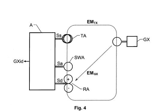
Figure 4 illustrates how a tag unit produces a modified al-
ternating electromagnetic field and how the propo-
sed apparatus may receive a signal based there-
on;
Figure 5 shows the processing unit according to one embo-
diment of the invention;
Figures 6a-f represent graphs exemplifying the signal flow in
the apparatus according to the embodiment of the
invention shown in Figure 5; and
Figure 7 illustrates, by means of a flow diagram, the gene-
ral method according to the invention.
DESCRIPTION OF PREFERRED EMBODIMENTS OF THE IN-
VENTION
We refer initially to Figure 1, which shows a general overview of
an apparatus A for contactless identification of a tag unit GX
according to the invention.
The tag unit GX is presumed to include circuitry configured to
modify an alternating electromagnetic field EM-rx within which
the tag unit GX is located. Typically, to this aim, the tag unit GX
contains at least one resonance circuit.
The apparatus A includes a transmitter circuit TX, a transmitter
antenna TA, a receiver circuit RX, a receiver antenna RA and a
processing unit PU.
The transmitter circuit TX is configured to generate an electric
CA 02887413 2015-04-08
WO 2014/081383
PCT/SE2013/051379
7
source signal Ss and, via the transmitter antenna TA connected
thereto, emit an alternating electromagnetic field EMI-x from the
apparatus A, which alternating electromagnetic field EM-rx cor-
responds to the electric source signal Ss.
The receiver antenna RA is configured to register the alternating
electromagnetic field EM-1- x and any modifications thereof EMGx
that are caused by the presence of a tag unit GX within a range
of operation from the apparatus A. The receiver circuit RX is
connected to the receiver antenna RA. Thereby, receiver circuit
RX is further configured to produce an electric detection signal
Sd in response to the alternating electromagnetic field EMI-x,
and EMGx registered by the receiver antenna RA.
The processing unit PU is configured to receive the electric de-
tection signal Sd. Based on the electric detection signal Sd, the
processing unit PU is configured to discriminate identification
data GXid of any tag unit GX having modified the alternating
electromagnetic field EMGx.
To provide an aiding signal component Sa (i.e. a reference sig-
nal) to the processing unit PU, and thus facilitate discriminating
the identification data GXid, the receiver antenna RA is arran-
ged relative to the transmitter antenna TA and a potential tag
unit GX, such that a portion of the emitted alternating elect-
romagnetic field EM-rx always reaches the receiver antenna RA
unmodified, irrespective of whether or not a tag unit GX is pre-
sent within the range of operation. Figures 2, 3 and 4 show dif-
ferent examples how this may be accomplished.
Thus, more precisely, the processing unit PU is configured to
discriminate the identification data GXid based on the electric
detection signal Sd and by utilizing the aiding signal component
Sa, i.e. a signal originating from the unmodified portion of the al-
ternating electromagnetic field EMI-x.
Referring now to Figure 2, we see a part of an apparatus A ac-
cording to a first embodiment of the invention.
CA 02887413 2015-04-08
WO 2014/081383
PCT/SE2013/051379
8
The receiver antenna RA is arranged in a transmission path for
the emitted alternating electromagnetic field EMTx between the
transmitter antenna (not shown) and a potential tag unit GX
within the range of operation. This means that the receiver an-
tenna RA will register the emitted alternating electromagnetic
field EMTx as well as any modifications thereof EMGx caused by
the tag unit GX.
The receiver antenna RA here has at least two loops of antenna
coil, where a first loop + is twisted 180 degrees and in phase
__ opposition with a second loop -. The first and second loops +/-
are arranged in the transmission path for the emitted alternating
electromagnetic field EMTx, such that the emitted unmodified al-
ternating electromagnetic field EMTx that passes through both
the first and second loops +/- is cancelled out. However, the tag
__ unit GX is expected to be located such that the distance bet-
ween the tag unit GX and the first loop + is always different from
the distance between the tag unit GX and the second loop -. In
other words, the apparatus A is positioned such that the tag unit
GX may only be located where its distance to the receiver an-
__ tenna RA is shorter than its distance to the transmitter antenna.
I.e., in Figure 2, the tag unit is located on the general right hand
side. As a result, the modified alternating electromagnetic field
EMGx will not cancel out in the receiver antenna, and can there-
fore be detected by the apparatus A.
__ Moreover, the apparatus A preferably has an auxiliary antenna
SWA, which is configured to receive the emitted unmodified alte-
rnating electromagnetic field EMTx to represent the aiding signal
component Sa. The aiding signal component Sa is then forwar-
ded to the processing unit PU for use when discriminating the
__ identification data GXid.
Figure 3 shows an apparatus A according to a second embodi-
ment of the invention. Here, the receiver antenna RA contains at
least one first antenna coil RA1 and at least one second anten-
na coil RA2.
CA 02887413 2015-04-08
WO 2014/081383
PCT/SE2013/051379
9
The at least one first antenna coil RA1 is arranged on an opera-
tive side of the transmitter antenna TA, which in Figure 3, is the
general right hand side. The at least one first antenna coil RA1
is further located in the transmission path for the alternating
electromagnetic field between the transmitter antenna TA and a
potential tag unit GX within the range of operation on the opera-
tive side of the transmitter antenna TA. Consequently, the at
least one first antenna coil RA1 may receive both the emitted
unmodified alternating electromagnetic field EMI-x and any
modifications thereof EMGx due to the presence of a tag unit GX.
The at least one second antenna coil RA2 is arranged on a pas-
sive side of the transmitter antenna TA, which passive side is
opposite to the operative side. Thereby, the at least one second
antenna coil RA2 is configured to receive an unmodified portion
of the alternating electromagnetic field EM-rx. Thus, the at least
one second antenna coil RA2 can provide the aiding signal
component Sa to the receiver circuit RX.
Figure 4 shows the apparatus A according to one embodiment of
the invention. As described above, the apparatus A emits an al-
ternating electromagnetic field EM-rx via a transmitting antenna
TX. The alternating electromagnetic field EM-1- x covers an ope-
rative range from the apparatus A. We assume that a tag unit
GX is located within the operative range, and thus produces a
modified alternating electromagnetic field EMGx in response to
the emitted alternating electromagnetic field EM-r.
This modification may involve phase-shift modulating of a data
signal onto the emitted alternating electromagnetic field EM-rx,
where the data signal has a rate substantially lower than the fre-
quency of the emitted alternating electromagnetic field EM-r,
say a factor 100 lower, and the data signal represents an iden-
tification of the tag unit GX. Nevertheless, due to a resonance
circuit in the tag unit GX, the modification therein typically also
results in a -90 degrees phase shift of the emitted alternating
electromagnetic field EMTx. The emitted alternating electromag-
CA 02887413 2015-04-08
WO 2014/081383
PCT/SE2013/051379
netic field EMI-x may thus be regarded as a -90 phase shifted,
single-side-band modulated signal propagating towards the ap-
paratus A resulting from a reflection of the emitted alternating
electromagnetic field EM-rx in the tag unit GX.
5 The operative range is defined as the distance from the appara-
tus A within which a tag unit GX must be located in order to en-
able the apparatus A to discriminate identification data GXid
from its modified alternating electromagnetic field EMGx. Since
the tag unit GX is a truly passive element, and the power level
10 of the electromagnetic field decreases with a cubic relationship
to the distance, the operative range is relatively short. Neverthe-
less, a power level difference of 80-100 dBA between the EMTx
and EMGx fields is normally acceptable. This is explained by the
fact that, as explained above, the emitted alternating electro-
magnetic field EMI-x cancels out in the receiver antenna RA,
whereas the modified alternating electromagnetic field EMGx
does not.
An auxiliary antenna SWA in the apparatus A is configured to re-
ceive an unmodified version of the emitted alternating electro-
magnetic field EM-rx and forward a corresponding aiding signal
component Sa to the processing unit PU therein. Further, the
processing unit PU is configured to derive the aiding signal com-
ponent Sa to represent a phase angle of the electric source sig-
nal Ss as a function of time, and finally discriminate the identifi-
cation data GXid based on the phase variations of the electric
detection signal Sd relative to the phase angle of the electric
source signal Ss.
Preferably, the transmitter antenna TA and the receiver antenna
RA are co-located and arranged relative to one another, such
that during normal operation of the apparatus A, a distance bet-
ween the transmitter antenna TA and the receiver antenna RA is
shorter than an expected distance between the tag unit GX and
any of the transmitter antenna TA and the receiver antenna RA.
This relationship between said distances can be guaranteed by
CA 02887413 2015-04-08
WO 2014/081383
PCT/SE2013/051379
11
placing the transmitter and receiver antennas TA and RA behind
an antenna dome, where the distance from the respective an-
tennas and the dome exceeds the distance between the trans-
mitter antenna TA and the receiver antenna RA. Namely, there-
by, any tag unit TX must always be further away from the trans-
mitter and receiver antennas TA and RA than the distance bet-
ween the two of them. Such a design is, of course, enabled by
the proposed use of the aiding signal component Sa. The
relatively short distance between the transmitter and receiver
antennas TA and RA allows a highly compact and small-sized
apparatus A, especially compared to a design where the trans-
mitter and receiver antennas are arranged on different sides of
aisle (or similar) along which individuals carrying the tag units
GX proceed.
Figure 5 shows a schematic block diagram of the processing
unit PU according to one embodiment of the invention, and Figu-
res 6a to 6f represent graphs illustrating the different signals in
the processing unit PU.
Figure 6a shows the electric source signal Ss as a function of
the phase angle cp. The electric source signal Ss is fed into a
sampling circuit SC of the processing unit PU. In this embodi-
ment, the sampling circuit SC, in turn, includes a phase shifting
unit PPh, which is configured to delay the electric source signal
Ss so as to produce a delayed signal Sa_90., which corresponds
to a -90 degrees phase shift of the electric source signal Ss.
The delayed signal Sa_90., which is illustrated in Figure 6b as a
function of time t, is fed to each of a first switch unit T1 and a
second switch unit T2 in the sampling circuit SC. Both the switch
units T1 and T2 receive the electric detection signal Sd from the
receiver circuit RX. The first switch unit T1 is configured to be
closed briefly, e.g. via a diode circuit and an associated capaci-
tor CI, and thus pass through the electric detection signal Sd at
time instances t1, t3, tn
when the delayed signal Sa_90.
has its maximum positive amplitude. Figure 6c represents a
CA 02887413 2015-04-08
WO 2014/081383
PCT/SE2013/051379
12
signal Sa_goop, which reflects this operation of the first switch
unit T1 as a function of time t. Analogously, the second switch
unit T2 is configured to be closed briefly, e.g. via a diode circuit
and an associated capacitor C2, and thus pass through the
electric detection signal Sd at time instances t2,..., ti+i when the
delayed signal Sa_go has its maximum negative amplitude. Fi-
gure 6d represents a signal Sa_gooN, which reflects this operation
of the second switch unit T2 as a function of time t.
Thus, the switch units T1 and 12 produce a respective series of
sampled values Sdps and SdNs from the electric detection signal
Sd. Due to the phase shift between the electric detection signal
Sd) and the emitted electric source signal Ss, the time instances
t2, t3, ===, t1, ti+1, ===, tn when the electric detection signal Sd is
sampled correspond to the phase angles (I) where the electric
source signal Ss has zero-line passages. In other words, the
processing unit PU is configured to exclusively analyze the
electric detection signal Sd at predetermined phase angle shifts
relative to the electric source signal Ss. As explained below, this
analysis forms a basis for discriminating the identification data
GXid.
More precisely, according to this embodiment of the invention,
the sample values Sdps and SdNs are fed into a differential am-
plifier D, such that the values Sdps from the first switch unit T1
are associated with a positive sign and the values SdNs from the
second switch unit 12 are associated with a negative sign. In
response thereto, the differential amplifier D produces a resul-
tant signal R, which is bandpass filtered in a filter unit BPF ha-
ving a passband matched to a resonance frequency of the tag
unit GX. Consequently, based on the resultant signal R, the filter
unit BPF produces identification data GXid, for instance indi-
cating identity information pertaining to an animal carrying the
tag unit GX.
Preferably, the apparatus A contains, or is communicatively con-
nected to, a memory unit M storing a computer program product,
CA 02887413 2015-04-08
WO 2014/081383
PCT/SE2013/051379
13
which contains software for controlling the apparatus A to
perform the above-described actions when the computer pro-
gram product is run on a processor in the processing unit PU.
In order to sum up, we will now describe the general method ac-
cording to the invention with reference to the flow diagram in
Figure 7.
In a first step 710, the transmitter circuit TX generates an elect-
ric source signal Ss and emits a corresponding alternating elect-
romagnetic field EMTx from the apparatus A via a transmitter
antenna TA.
A step 720, then registers the alternating electromagnetic field
EMTx as well as any modifications thereof EMGx due to a tag unit
within the range of operation from the apparatus A. In parallel
with step 720, a step 730 registers an unmodified alternating
electromagnetic field EMTx representing a basis for the aiding
signal component Sa.
Thereafter, a step 740 discriminates the identification data GXid
from the alternating electromagnetic fields EMTx and EMGx re-
gistered in step 720 by utilizing the aiding signal component Sa
derived in step 730. Subsequently, the procedure loops back to
step 710.
All of the process steps, as well as any sub-sequence of steps,
described with reference to Figure 7 above may be controlled by
means of a programmed computer apparatus. Moreover, al-
though the embodiments of the invention described above with
reference to the drawings comprise computer apparatus and
processes performed in computer apparatus, the invention thus
also extends to computer programs, particularly computer pro-
grams on or in a carrier, adapted for putting the invention into
practice. The program may be in the form of source code, object
code, a code intermediate source and object code such as in
partially compiled form, or in any other form suitable for use in
the implementation of the process according to the invention.
CA 02887413 2015-04-08
WO 2014/081383
PCT/SE2013/051379
14
The program may either be a part of an operating system, or be
a separate application. The carrier may be any entity or device
capable of carrying the program. For example, the carrier may
comprise a storage medium, such as a Flash memory, a ROM
(Read Only Memory), for example a DVD (Digital Video/Versatile
Disk), a CD (Compact Disc) or a semiconductor ROM, an EP-
ROM (Erasable Programmable Read-Only Memory), an EEPROM
(Electrically Erasable Programmable Read-Only Memory), or a
magnetic recording medium, for example a floppy disc or hard
disc. Further, the carrier may be a transmissible carrier such as
an electrical or optical signal which may be conveyed via elect-
rical or optical cable or by radio or by other means. When the
program is embodied in a signal which may be conveyed directly
by a cable or other device or means, the carrier may be consti-
tuted by such cable or device or means. Alternatively, the carrier
may be an integrated circuit in which the program is embedded,
the integrated circuit being adapted for performing, or for use in
the performance of, the relevant processes.
The term "comprises/comprising" when used in this specification
is taken to specify the presence of stated features, integers,
steps or components. However, the term does not preclude the
presence or addition of one or more additional features, integers,
steps or components or groups thereof.
The invention is not restricted to the described embodiments in
the figures, but may be varied freely within the scope of the
claims.