Note: Descriptions are shown in the official language in which they were submitted.
CA 02887421 2015-04-07
WO 2014/055880
PCT/US2013/063483
SYSTEMS AND METHODS FOR AMPLIFYING LIGHT
Cross-Reference to Related Application
This application claims the benefit of, and priority to, U.S. Provisional
Patent Application
No. 61/710,424, filed October 5, 2012, the contents of which are incorporated
by reference.
Field of the Invention
The invention generally relates to systems and methods for amplifying light.
0 Background
Optical systems are used in a variety of applications that require amplified
light at a
particular wavelength, such as optical communication networks, medical
imaging, and
atmospheric remote sensing. Amplified light is provided by a light source that
includes an optical
amplifier. An optical amplifier amplifies light by passing it through a gain
medium. The gain
5 medium is a material that increases the power of light by stimulated
emission when supplied
with energy. Where laser light is desired, the gain medium is positioned
between a pair of
mirrors known as an optical cavity. Input light resonates between the mirrors
while being re-
amplified by the gain medium until the lasing threshold is surpassed and laser
light is produced.
A gain medium has a peak gain associated with a transition frequency of its
constituent
elements. Light having a wavelength at the peak gain is more readily and more
robustly
amplified than light at other wavelengths. Consequently, the lasing threshold
is lowest at the
peak gain.
Where an optical system requires a particular wavelength of amplified light,
the light
source may include a tunable optical filter. Amplified light of a selected
wavelength is obtained
by tuning the filter to that wavelength and sending the light into the gain
medium with sufficient
input power to achieve a desired output power. However, while providing light
of a selected
wavelength, tunable optical filters also emit a low background level of light
across a broad
spectrum of wavelengths. When the input power is high enough to successfully
amplify a
selected frequency not at peak gain, the input power of background light at
the peak gain can
;0 surpass the lasing threshold, resulting in undesired lasing, i.e.,
parasitic lasing. This so-called
1
CA 02887421 2015-04-07
WO 2014/055880
PCT/US2013/063483
parasitic lasing leaches energy from the system, creates spurious spectral
peaks, adds noise to
optical signals, and diminishes the power of amplified light at the selected
wavelength.
As a consequence, the useful range of a tunable filter is limited. For
existing light sources
to be used effectively, the tunable optical filter must be kept within a
narrow tuning range
surrounding the peak gain of the optical amplifier. Thus, once a light source
is deployed in an
optical system, use of the entire system is restricted by the gain medium of
the optical amplifier
to a narrow range of wavelengths defined by a peak gain of the gain medium. A
variety of
optical applications in medicine, research, and communication require a range
of wavelengths of
light broader than existing optical systems can handle and performing these
applications requires
0 multiple optical systems, each built around its own gain medium.
Summary
The invention provides optical amplifier devices, systems, and methods that
suppress
parasitic lasing. Devices and methods of the invention suppress parasitic
lasing by employing
5 wavelength-dependent reflectivity that inhibits reflection at a peak gain
of a gain medium
without inhibiting reflection at wavelengths not at the peak gain. Devices and
methods of the
invention inhibit reflection of light near the peak gain and even when a
tunable filter is used, as
low level background light from the filter does not exceed the lasing
threshold of the gain
medium. This allows the optical amplifier to amplify light across a broad
range of wavelengths
without parasitic lasing, thereby increasing the useable range of a tunable
optical filter. In this
manner, light at wavelengths not at a peak gain can be used effectively, and
the gain medium of
an optical amplifier does not limit use of a system to a narrow range of
wavelengths associated
with a peak gain of the gain medium. Thus, a single optical system according
to the invention
can be used for applications that require a broad range of wavelengths.
In certain aspects, the invention provides a method for amplifying light that
includes
transmitting light through a gain medium in which the light includes
wavelengths at the peak
gain of the gain medium and wavelengths not at the peak gain. Substantially
all reflection of the
light at the peak gain wavelengths is inhibited, thereby allowing
amplification of the light not at
the peak gain. The application provides techniques to selectively inhibit
reflection at the peak
;0 gain wavelengths and not inhibit reflection at wavelengths not at the
peak gain, preferably not
inhibiting reflection at wavelengths both above and below the peak gain. In
certain
2
CA 02887421 2015-04-07
WO 2014/055880
PCT/US2013/063483
embodiments, the invention utilizes surface coatings that inhibit reflection
in a wavelength-
dependent matter, for example, inhibiting substantially all reflection at a
peak gain. In certain
embodiments, a gain medium is included that is solid with at least one surface
facet that
transmits or reflects light. Materials for use with systems and methods of the
invention can be
used to coat a facet of a gain medium or a surface in an optical path such as
a mirror. A coated
mirror can be any mirror within the optical path of a light source, such as
one of the mirrors in a
tunable etalon or either reflector in an optical cavity. In some embodiments,
systems and
methods of the invention use a wavelength-dependent mirror as an output
coupler for a laser or
optical amplifier.
0 By inhibiting substantially all reflection at the peak gain of a
gain medium, the input
power of an optical amplifier can be increased. Systems and methods of the
invention diminish
the power of those wavelengths of light corresponding to a lowest lasing
threshold of the gain
medium, allowing light of a selected wavelength to be usably amplified without
parasitic lasing.
By suppressing parasitic lasing in the gain medium, devices and methods of the
invention allow a
5 tunable optical filter to be tuned across a range of wavelengths greater
than previously possible
for a given gain medium. Methods of the invention can be used with any gain
medium known in
the art including, for example and without limitation, a semiconductor gain
medium as found, for
example, in a semiconductor optical amplifier or a booster optical amplifier.
In certain aspects, the invention provides a semiconductor optical amplifier
including a
semiconductor gain medium and a material that inhibits substantially all
reflection at the peak
gain, thus allowing the gain medium to amplify light at wavelengths not at the
peak gain without
parasitic lasing. The material can be provided as a mirror or as one of the
facets of a solid gain
medium. For example, an end facet of a semiconductor optical amplifier or
booster optical
amplifier or a mirror of an optical cavity can be coated with the material.
In other aspects, the invention provides a system for producing coherent
light, including
an optical amplifier with a reflector in optical communication with the
optical amplifier in which
the reflector inhibits reflection of light at the peak gain and reflects light
at wavelengths not at
the peak gain, thereby suppressing parasitic lasing. The optical amplifier
produces coherent near
infrared light from incident light delivered by a filter module in optical
connection to the optical
;0 amplifier. Preferably, the reflector is an output coupler and the
optical amplifier is a
3
CA 02887421 2015-04-07
WO 2014/055880
PCT/US2013/063483
semiconductor optical amplifier. In certain embodiments, the system includes
an output
mechanism configured to be coupled to a fiber optic interferometer or other
imaging device.
Systems and methods of the invention may be employed in any industry or
application
including, for example, medical imaging. In certain embodiments, the invention
provides
systems and methods for providing light for imaging tissue. For example,
systems of the
invention can generate coherent, near-infrared light without parasitic lasing
for use in optical
coherence tomography (OCT).
Brief Description of the Drawings
0 FIG. 1 illustrates photon emission.
FIG. 2 is a schematic diagram of a semiconductor optical amplifier.
FIG. 3 shows the emission wavelengths of semiconductor materials.
FIG. 4 is a specification sheet for a booster optical amplifier.
FIG. 5 is a gain curve for a booster optical amplifier.
5 FIG. 6 shows an optical component.
FIG. 7 is a diagram of a laser.
FIG. 8 shows a gain curve showing a peak gain.
FIG. 9 shows wavelength dependent reflectivity of a material of the invention.
FIG. 10 is a diagram of a light path within an optical filter.
FIG. 11 is a diagram of an optical system according to certain embodiments of
the
invention.
FIG. 12 is a high-level diagram of a system for optical coherence tomography.
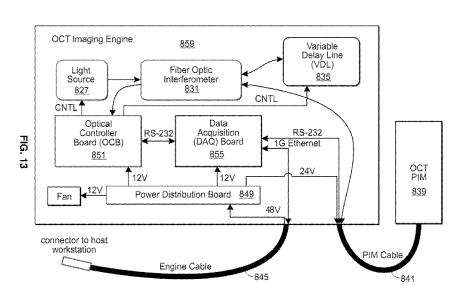
FIG. 13 is a schematic diagram of the imaging engine of an OCT system.
FIG. 14 is a diagram of a light path in an OCT system.
FIG. 15 shows the organization of a patient interface module in an OCT system.
Detailed Description
The invention generally provides systems and methods for amplifying light
using a gain
component that includes a gain medium, in which the light includes wavelengths
at a peak gain
;0 of the gain medium and wavelengths not at the peak gain. Any device that
amplifies light that is
compatible with systems and methods of the invention may be used as the gain
component, such
4
CA 02887421 2015-04-07
WO 2014/055880
PCT/US2013/063483
as, for example and without limitation, a semiconductor optical amplifier, a
laser, or a booster
optical amplifier. Systems and methods of the invention also include one or
more components
within an optical path that selectively inhibit reflection in a wavelength
dependent fashion.
Reflection can be inhibited by any method known in the art such as a coating
on a surface. In
certain embodiments, a mirror is provided having a surface coated to reflect
light in a wavelength
dependent manner.
Systems of the invention include gain components, components for wavelength
dependent reflection, and any other compatible component known in the art
including optical
filters, fibers, coupling mechanisms, and interferometers. In certain
embodiments, an optical
0 filter is a tunable optical filter. Systems of the invention may further
include other application-
specific hardware, firmware, and software. For example, in certain
embodiments, the invention
generally relates to a system to operate as a light source for optical
coherence tomography (OCT)
for use in imaging a lumen biological tissue.
Systems of the invention generally include at least one gain component that
amplifies the
5 power of light that is transmitted through it. When light interacts with
material, a few outcomes
may be obtained. Light can be transmitted through the material unaffected or
reflect off of a
surface of the material. Alternatively, an incident photon of light can
exchange energy with an
electron of an atom within the material by either absorption or stimulated
emission. As shown in
FIG. 1, if the photon is absorbed, the electron 101 transitions from an
initial energy level El to a
higher energy level E2 (in three-level systems, there is a transient energy
state associated with a
third energy level E3).
When electron 101 returns to ground state El, a photon 105 is emitted. When
photons are
emitted, there is net increase in power of light within the gain medium. In
stimulated emission,
an electron emits energy AE through the creation of a photon of frequency vi2
and coherent with
the incident photon. Two photons are coherent if they have the same phase,
frequency,
polarization, and direction of travel. Equation 1 gives the relationship
between energy change AE
and frequency v12:
(1) AE=h1/12
;0 where h is Plank's constant. Light produced this way can be temporally
coherent, i.e., having a
single location that exhibits clean sinusoidal oscillations over time.
5
CA 02887421 2015-04-07
WO 2014/055880
PCT/US2013/063483
An electron can also release a photon by spontaneous emission. Amplified
spontaneous
emission (ASE) in a gain medium produces spatially coherent light, e.g.,
having a fixed phase
relationship across the profile of a light beam.
Emission prevails over absorption when light is transmitted through a material
having
more excited electrons than ground state electrons¨a state known as a
population inversion. A
population inversion can be obtained by pumping in energy (e.g., current or
light) from outside.
Where emission prevails, the material exhibits a gain G defined by Equation 2:
(2) G=10 Logio (Pout.- /P 1 dB
in,
0 where Pout and Plu are the optical output and input power of the gain
medium.
Systems of the invention include one or more gain components for use as a
light source.
A gain component, generally, refers to any device known in the art capable of
amplifying light
such as an optical amplifier, laser, or any component employing a gain medium.
A gain medium
is a material that increases the power of light that is transmitted through
the gain medium.
5 Exemplary gain mediums include crystals (e.g., sapphire), doped crystals
(e.g., yttrium
aluminum garnet, yttrium orthovanadate), glasses such as silicate or phosphate
glasses, gasses
(e.g., mixtures of helium and neon, nitrogen, argon, or carbon monoxide),
semiconductors (e.g.,
gallium arsenide, indium gallium arsenide), and liquids (e.g., rhodamine,
fluorescein).
A gain component can be an optical amplifier or a laser. An optical amplifier
is a device
that amplifies an optical signal directly, without the need to first convert
it to an electrical signal.
An optical amplifier generally includes a gain medium (e.g., without an
optical cavity), or one in
which feedback from the cavity is suppressed. Exemplary optical amplifiers
include doped
fibers, bulk lasers, semiconductor optical amplifiers (SOAs), and Raman
optical amplifiers. In
doped fiber amplifiers and bulk lasers, stimulated emission in the amplifier's
gain medium causes
amplification of incoming light. In semiconductor optical amplifiers (SOAs),
electron-hole
recombination occurs. In Raman amplifiers, Raman scattering of incoming light
with phonons
(i.e., excited state quasiparticles) in the lattice of the gain medium
produces photons coherent
with the incoming photons.
Doped fiber amplifiers (DFAs) are optical amplifiers that use a doped optical
fiber as a
;0 gain medium to amplify an optical signal. In a DFA, the signal to be
amplified and a pump laser
are multiplexed into the doped fiber, and the signal is amplified through
interaction with the
6
CA 02887421 2015-04-07
WO 2014/055880
PCT/US2013/063483
doping ions. The most common example is the Erbium Doped Fiber Amplifier
(EDFA),
including a silica fiber having a core doped with trivalent Erbium ions. An
EDFA can be
efficiently pumped with a laser, for example, at a wavelength of 980 nm or
1.480 nm, and
exhibits gain, e.g., in the 1.550 nm region. An exemplary EDFA is the Cisco
ONS 15501 EDFA
from Cisco Systems, Inc. (San Jose, CA).
Semiconductor optical amplifiers (SOAs) are amplifiers that use a
semiconductor to
provide the gain medium. FIG. 2 is a schematic diagram of a semiconductor
optical amplifier.
Input light 213 is transmitted through gain medium 201 and amplified output
light 205 is
produced. An SOA includes n-cladding layer 217 and p-cladding layer 209. An
SOA typically
0 includes a group III-V compound semiconductor such as GaAs/AlGaAs,
InP/InGaAs,
InP/InGaAsP and InP/InAlGaAs, though any suitable semiconductor material may
be used. FIG.
3 shows the emission wavelengths of semiconductor materials.
A typical semiconductor optical amplifier includes a double heterostructure
material with
n-type and p-type high band gap semiconductors around a low band gap
semiconductor. The
5 high band gap layers are sometimes referred to as p-cladding and n-
cladding layers (having, by
definition, more holes than electrons and more electrons than holes,
respectively). The carriers
are injected into the gain medium where they recombine to produce photons by
both spontaneous
and stimulated emission. The cladding layers also function as waveguides to
guide the
propagation of the light signal. Semiconductor optical amplifiers are
described in Dutta and
Wang, Semiconductor Optical Amplifiers, 297 pages, World Scientific Publishing
Co. Pte. Ltd.,
Hackensack, NJ (2006), the contents of which are hereby incorporated by
reference in their
entirety.
Booster Optical Amplifiers (BOAs) are single-pass, traveling-wave amplifiers
that only
amplify one state of polarization generally used for applications where the
input polarization of
the light is known. Since a BOA is polarization sensitive, it can provide
desirable gain, noise,
bandwidth, and saturation power specifications. In some embodiments, a BOA
includes a
semiconductor gain medium (i.e., is a class of SOA). In certain embodiments, a
BOA includes
an InP/InGaAsP Multiple Quantum Well (MQW) layer structure. The input and
output of BOA
can be coupled to one or more waveguides on an optical amplifier chip. FIG. 4
is a specification
;0 sheet and FIG. 5 is a gain curve for a COTS booster optical amplifier.
7
CA 02887421 2015-04-07
WO 2014/055880
PCT/US2013/063483
As shown in FIG. 6, optical amplifier components can be provided in a standard
14-pin
butterfly package with either single mode fiber (SMF) or polarization maintain
fiber (PMF)
pigtails, which can be terminated with any fixed connection (FC) connector
such as an angled
physical connection (FC/APC) connector. Optional polarization-maintaining
isolators can be
provided at the input, output or both. In certain embodiments, the invention
provides a
wavelength dependent reflector as a reflective surface with an optical
amplifier, such as a mirror
or one of the facets of the gain medium.
A laser generally is an optical amplifier in which the gain medium is
positioned within
an optical resonator (i.e., an optical cavity) as diagramed in FIG. 7. An
optical resonator is an
0 arrangement of mirrors that forms a standing wave cavity resonator for
light waves, e.g., a pair of
mirrors on opposite ends of the gain medium and facing each other. The pair
includes high
reflector 717 and output coupler 705 surrounding gain medium 701. Incident
light 721 reflects
between the mirrors creating standing wave 713. Some light is emitted as laser
beam 709.
Where laser light is desired, the gain medium is positioned in an optical
cavity. The optical
5 cavity confines light in the gain medium, thereby feeding amplified light
back through the
amplification medium allowing it to be amplified again. Input light resonates
between the
mirrors while being re-amplified by the gain medium until the lasing threshold
is surpassed and
laser light is produced. This results in a positive feedback cycle tending to
increase the gain G of
the optical amplifier.
In a laser, one of the mirrors of the optical cavity is generally known as the
high reflector
while the other is the output coupler. Typically, the output coupler is
partially transparent and
emits the output laser beam. In certain embodiments, the invention provides a
wavelength
dependent reflector as a reflective surface with laser, such as one of the
mirrors (e.g., the output
coupler) or one of the facets of the gain medium.
A laser can be provided, for example, as a COTS component in a 14-pin
butterfly
package with either SMF or PMF pigtails. One such exemplary laser is the 980
nm pump laser
module with Bragg grating sold under the mark POWERPURE 1998 PLM, available
from
Avanex Corporation (Fremont, CA).
In certain embodiments, a gain component such as an optical amplifier or a
laser
;0 amplifies light in a frequency-specific manner. A gain component
includes a gain medium
8
CA 02887421 2015-04-07
WO 2014/055880
PCT/US2013/063483
having a gain coefficient g (gain per unit length) that is a function of the
optical frequency of the
incident signal co. The gain coefficient at a given frequency g(w) is given by
equation 3:
(3) g(w)=g0/(1+(w-wo)2T2+P/Ps)
where go is the peak gain of the medium, P is the optical power of the signal
being amplified, Ps
is the saturation power of the gain medium, wo is an atomic transition
frequency of the medium,
and T is a dipole relaxation time. Where incident light has a frequency co, a
gain medium has a
gain coefficient g(w) and gain is given by Equation 4:
(4) G(o))=exp[g(w)L]
0
where L is a length of the gain medium.
The power of amplified light at a distance z from the input end of a gain
medium is given
by Equation 5:
(5) P(z) = Pmexp(gz)
5
Gain coefficient g has an inverse square relationship to (o-wo) (see Equation
3) and
power P(z) is exponentially related to gain coefficient g. Thus, the gain of a
gain medium is
higher for optical frequencies co closer to 00. FIG. 8 shows gain as a
function of wavelength for
a typical gain medium. As shown by the peak of the gain curve, the gain medium
has a "peak
gain".
If light of various wavelengths is amplified by the medium (at powers well
below the
saturation power Ps of the gain medium), light having a wavelength at or near
the peak gain will
be amplified to greater powers than light having a wavelength not at or near
the peak gain.
For any wavelength of light, if the gain is greater than the loss, lasing can
result in which
the light is emitted as a laser beam. The conditions at which gain equals loss
is the lasing
threshold for a frequency of light. The lasing threshold is lowest at the peak
gain and light having
a wavelength at the peak gain is more readily and more robustly amplified than
other
wavelengths. Consequently, the gain medium most readily lases light at the
peak gain.
Where this lasing is unintended, it is known as parasitic lasing. If light
transmitted
;0 through the medium has sufficient power, wavelengths near the peak gain
will cross the lasing
threshold, causing lasing. This parasitic lasing leaches power from the
system, reduces coherence
9
CA 02887421 2015-04-07
WO 2014/055880
PCT/US2013/063483
length of signal light, and introduces noise into the signal. Due to the shape
of the gain curve in a
typical gain medium, parasitic lasing is problematic near the peak gain.
Devices and methods of the invention suppress parasitic lasing. In one
embodiment,
systems and methods of the invention suppress parasitic lasing by wavelength-
dependent
inhibition of reflection of light transmitted through a gain medium. By
providing a system
including a gain component and a wavelength dependent reflector, systems of
the invention can
provide amplified light of a selected wavelength without parasitic lasing at a
peak gain.
Materials for use with systems and methods of the invention can be employed to
selectively inhibit reflection at the peak gain and not inhibit reflection not
at the peak gain. In
0 certain embodiments inhibiting reflection is not at wavelengths both
above and below the peak
gain. Exemplary materials for use with systems and methods of the invention
include surface
coatings that inhibit reflection in a wavelength-dependent matter, for
example, inhibiting
substantially all reflection at a peak gain.
In general, a substrate with a reflective surface in which the surface is
coated presents
5 two reflective interfaces. The coated substrate provides an air/coating
interface and a
coating/substrate interface. A coating can be described in terms of physical
thickness t and
refractive index n, which together give an optical thickness nt of the
coating.
If the reflections from each interface are out of phase by 180 degrees (it
radians) then
those reflections will interfere destructively, cancelling each other out
(i.e., no light is reflected
and all of the light will be transmitted through the material). To eliminate
reflections at a
specific wavelength k, the optical thickness nt of the coating must be an odd
number of quarter
wavelengths k of light as shown in Equation 6.
(6) nt= N k/4,
where N = {1, 2, 3,. . . }. Generally, the refractive index n of the coating
should be the square
root of the refractive index of the substrate, as shown in Equation 7.
(7) ncoating="qnsubstrate
That is, where the substrate is glass, the coating should have a refractive
index n of about
;0 1.2 or so. Where multiple reflective coatings are used, cancellation is
a product of the relative
phase and intensity of the interfering beams. This cancellation can be
controlled by controlling
CA 02887421 2015-04-07
WO 2014/055880
PCT/US2013/063483
the relative optical thicknesses of the layers. For a given combination of
coatings, there are
typically two combinations of thicknesses that give zero reflectance at a
given wavelength.
Furthermore, two-layer antireflective coatings exhibit a curve of reflectance
as a function of
wavelength, generally having a V or U shape. This is shown in FIG. 9.
Any material suitable for any antireflective coating may be used. Exemplary
materials
include metals such as aluminum, silver, or gold or compounds such as
magnesium fluoride
(MgF2) in suitable thickness (e.g., single-layer quarter-wavelength coatings
or multi-layered).
Coated materials are sold under the trademark HEBBAR by CVI Melles Griot
(Albuquerque,
NM).
0 Coatings of the desired thickness can be fabricated by any method
known in the art
including, for example, vacuum deposition, electron bombardment vaporization,
plasma ion-
assisted deposition (PIAD), carbon vapor deposition, plasma vapor deposition,
and related
techniques. In vacuum deposition, a substrate is put in a vacuum chamber along
with a metal
crucible holding the coating substance. A high current (e.g., 100 A) is passed
through the coating
5 material, vaporizing it. Due to the vacuum, the vaporized material
disperses to the material to be
coated.
Materials for use with systems and methods of the invention can be used to
coat a facet of
a gain medium or a surface in an optical path such as a mirror. A coated
mirror can be any mirror
within the optical path of a light source, such as one of the mirrors in a
tunable etalon or a
reflector in a laser. In certain embodiments an output coupler of a
semiconductor optical
amplifier is coated with a wavelength dependent reflective material.
Where a mirror is coated with the wavelength dependent material, light at
wavelengths
not at the peak gain is reflected. In certain embodiments, the invention
provides a substrate with
a coated reflective surface (e.g., a coated mirror) that reflects light at
wavelengths both above
and below a peak gain. Inhibiting reflection in a wavelength dependent manner
can be used to
inhibit reflection at a peak gain of a gain medium of gain component thereby
suppressing
parasitic lasing. Thus, a light source according to the invention may be
operated to produce
amplified coherent light at wavelengths other than a peak gain of the gain
medium without
parasitic lasing near the peak gain.
;0 Where an optical system requires a particular wavelength of
amplified light, the light
source may include an optical filter module such as a tunable optical filter
in optical
11
CA 02887421 2015-04-07
WO 2014/055880
PCT/US2013/063483
communication with a gain component. FIG. 10 is a diagram of a light path
within an optical
filter comprising a Fabry-Perot etalon. Etalons are discussed in Laufer, G.,
Introduction to Optics
and Lasers in Engineering1996, 476 pages, Cambridge University Press,
Cambridge, UK, the
contents of which are incorporated by reference herein in their entirety (see,
e.g., 6.5 The
Fabry-Perot Etalon, pp. 156-162). Optical filters are discussed in U.S. Pat.
7,035,484; U.S. Pat.
6,822,798; U.S. Pat. 6,459,844; U.S. Pub. 2004/0028333; and U.S. Pub.
2003/0194165, the
contents of each of which are incorporated by reference herein in their
entirety.
An optical filter typically has a peak reflectivity and a background
reflectivity. The peak
reflectivity indicates an amount of light output (reflected) at the specified
wavelength, wherein a
0 desired wavelength can be set (in a tunable filter) by placing mirrors in
an etalon an appropriate
distance apart. The background reflectivity indicates an amount of light
output at wavelengths
other than the desired wavelength.
Typical filters might have, for example, a 20% peak reflectivity and an 0.02%
background reflectivity. The ratio of these number (103) defines the filter
contrast ratio,
5 expressed in decibels (dB) (here, 30 dB). Thus, if light of a certain
wavelength, say 1200 nm, is
intended, the filter will transmit light at 1200 nm as well as a broad
spectrum of light at lower
power in a ratio of 30 dB.
In some embodiments, systems of the invention include an optical filter that
can be tuned
to a desired wavelength, i.e., a tunable optical filter. Amplified light of a
selected wavelength is
obtained by tuning the filter to that wavelength and sending the light into
the gain medium with
sufficient input power to achieve a desired output power. An optical gain
component (e.g., SOA,
BOA, or laser) with a wavelength dependent material located in the light path
suppress low-level
background light across a broad spectrum of wavelengths. When the input power
is high enough
to successfully amplify a selected frequency not at peak gain, the input power
of background
light at the peak gain is suppressed, preventing parasitic lasing.
This allows the optical amplifier to amplify light across a broad range of
wavelengths
without parasitic lasing, thereby increasing the useable range of the tunable
optical filter. In this
manner, light at wavelengths not at a peak gain can be used effectively, and
the gain medium of
the optical amplifier does not limit use of a system to a narrow range of
wavelengths associated
;0 with a peak gain of the gain medium. In this fashion, the tunable range
of the tunable optical
filter is increased.
12
CA 02887421 2015-04-07
WO 2014/055880
PCT/US2013/063483
In general, the invention provides systems for producing coherent light that
include a gain
component such as an optical amplifier with a reflector in optical
communication with the optical
amplifier, in which the reflector inhibits reflection of light at the peak
gain and reflects light at
wavelengths not at the peak gain, thereby suppressing parasitic lasing. FIG.
11 is a diagram of an
optical system according to certain embodiments of the invention. Light 821 is
transmitted
through filter 825 and along light path 817. Gain component 813 produces
amplified coherent
light 805 with a wavelength dependent material 801 in the light path.
Amplified light 805 is sent
to downstream component 809 as needed (e.g., an interferometer). The gain
component
produces coherent near infrared light from incident light delivered by a
filter module in optical
0 connection to the gain component. Preferably, the reflector is an output
coupler and the gain
component is a semiconductor optical amplifier. Systems of the invention
further include any
other compatible component known in the art. Exemplary components include
interferometers,
couplers/splitters, controllers, and any other device known in the art.
Systems of the invention
may include input and output mechanisms, such as an output mechanism
configured to be
5 coupled to a fiber optic interferometer or other imaging device. An
optical system may include a
controller component. For example, systems can include the LDC1300B butterfly
LD/TEC
controller from Thorlabs (Newton, NJ). The LD/TEC controller and mount allows
a system to be
controlled by a computer. In certain embodiments, optical systems are
integrated into an optical
networking platform such as the Cisco ONS 15500 Dense Wave Division
Multiplexer.
In certain embodiments, the system includes an interferometer such as a fiber
optic
interferometer. An interferometer, generally, is an instrument used to
interfere waves and
measure the interference. Interferometry includes extracting information from
superimposed,
interfering waves. Any interferometer known in the art can be used. In certain
embodiments, an
interferometer is included in a Mach-Zehnder layout, for example, using single
mode optical
fibers. A Mach¨Zehnder interferometer is used to determine the relative phase
shift between two
collimated beams from a coherent light source and can be used to measure small
phase shifts in
one of the two beams caused by a small sample or the change in length of one
of the paths.
Measuring a phase change in one of two beams from a coherent light is employed
in
optical coherence tomography (OCT). Commercially available optical coherence
tomography
;0 systems are employed in diverse applications, including art conservation
and diagnostic
medicine, e.g., ophthalmology. Recently it has also begun to be used in
interventional cardiology
13
CA 02887421 2015-04-07
WO 2014/055880
PCT/US2013/063483
to help diagnose coronary artery disease. OCT systems and methods are
described in U.S. Pub.
2011/0152771; U.S. Pub. 2010/0220334; U.S. Pub. 2009/0043191; U.S. Pub.
2008/0291463; and
U.S. Pub. 2008/0180683, the contents of each of which are hereby incorporated
by reference in
their entirety.
Various lumen of biological structures may be imaged with aforementioned
imaging
technologies in addition to blood vessels, including, but not limited, to
vasculature of the
lymphatic and nervous systems, various structures of the gastrointestinal
tract including lumen of
the small intestine, large intestine, stomach, esophagus, colon, pancreatic
duct, bile duct, hepatic
duct, lumen of the reproductive tract including the vas deferens, vagina,
uterus and fallopian
0 tubes, structures of the urinary tract including urinary collecting
ducts, renal tubules, ureter, and
bladder, and structures of the head and neck and pulmonary system including
sinuses, parotid,
trachea, bronchi, and lungs.
In OCT, a light source delivers a beam of light to an imaging device to image
target
tissue. Within the light source is an optical amplifier and a tunable filter
that allows a user to
5 select a wavelength of light to be amplified. Wavelengths commonly used
in medical
applications include near-infrared light, for example, 800 nm for shallow,
high-resolution scans
or 1700 nm for deep scans.
Generally, there are two types of OCT systems, common beam path systems and
differential beam path systems, that differ from each other based upon the
optical layout of the
systems. A common beam path system sends all produced light through a single
optical fiber to
generate a reference signal and a sample signal whereas a differential beam
path system splits the
produced light such that a portion of the light is directed to the sample and
the other portion is
directed to a reference surface. The reflected light from the sample is
recombined with the signal
from the reference surface for detection. Common beam path interferometers are
further
described for example in U.S. Pat. 7,999,938; U.S. Pat. 7,995,210; and U.S.
Pat. 7,787,127, the
contents of each of which are incorporated by reference herein in its
entirety.
In a differential beam path system, amplified light from a light source is
input into an
interferometer with a portion of light directed to a sample and the other
portion directed to a
reference surface. A distal end of an optical fiber is interfaced with a
catheter for interrogation of
;0 the target tissue during a catheterization procedure. The reflected
light from the tissue is
recombined with the signal from the reference surface forming interference
fringes (measured by
14
CA 02887421 2015-04-07
WO 2014/055880
PCT/US2013/063483
a photovoltaic detector) allowing precise depth-resolved imaging of the target
tissue on a micron
scale. Exemplary differential beam path interferometers are Mach¨Zehnder
interferometers and
Michelson interferometers. Differential beam path interferometers are further
described for
example in U.S. Pat. 7,783,337; U.S. Pat. 6,134,003; and U.S. Pat. 6,421,164,
the contents of
each of which are incorporated by reference herein in its entirety.
In certain embodiments, the invention provides a differential beam path OCT
system with
intravascular imaging capability as illustrated in FIG. 12. For intravascular
imaging, a light
beam is delivered to the vessel lumen via a fiber-optic based imaging catheter
826. The imaging
catheter is connected through hardware to software on a host workstation. The
hardware
0 includes an imagining engine 859 and a handheld patient interface module
(PIM) 839 that
includes user controls. The proximal end of the imaging catheter is connected
to PIM 839, which
is connected to an imaging engine as shown in FIG. 12.
As shown in FIG. 13, the imaging engine 859 (e.g., a bedside unit) houses a
power
supply 849, light source 827, interferometer 931, and variable delay line 835
as well as a data
5 acquisition (DAQ) board 855 and optical controller board (OCB) 854. A PIM
cable 841
connects the imagine engine 859 to the PIM 839 and an engine cable 845
connects the imaging
engine 859 to the host workstation.
FIG. 14 shows light path in an exemplary embodiment of the invention. Light
for image
capture originates within the light source 827. This light is split between an
OCT interferometer
905 and an auxiliary interferometer 911. The OCT interferometer generates the
OCT image
signal and the auxiliary, or "clock", interferometer characterizes the
wavelength tuning
nonlinearity in the light source and generates a digitizer sample clock.
In certain embodiments, each interferometer is configured in a Mach-Zehnder
layout and
uses single mode optical fibers to guide the light. Fibers are connected via
either LC/APC
connectors or protected fusion splices. By controlling the split ratio between
the OCT and
auxiliary interferometers with splitter 901, the optical power in the
auxiliary interferometer is
controlled to optimize the signal in the auxiliary interferometer. Within the
auxiliary
interferometer, light is split and recombined by a pair of 50/50
coupler/splitters.
Light directed to the main OCT interferometer is also split by splitter 917
and
;0 recombined by splitter 919 with an asymmetric split ratio. The majority
of the light is guided into
the sample path 913 and the remainder into a reference path 915. The sample
path includes
CA 02887421 2015-04-07
WO 2014/055880
PCT/US2013/063483
optical fibers running through the PIM 839 and the imaging catheter 826 and
terminating at the
distal end of the imaging catheter where the image is captured.
Typical intravascular OCT involves introducing the imaging catheter into a
patient's
target vessel using standard interventional techniques and tools such as a
guidewire, guide
catheter, and angiography system. When operation is triggered from the PIM or
control console,
the imaging core of the catheter rotates while collecting image data that it
delivers to the console
screen. Rotation is driven by spin motor 861 while translation is driven by
pullback motor 865,
shown in FIG. 15 Blood in the vessel is temporarily flushed with a clear
solution while a motor
translates the catheter longitudinally through the vessel.
0 In certain embodiments, the imaging catheter has a crossing profile
of 2.4F (0.8mm) and
transmits focused OCT imaging light to and from the vessel of interest.
Embedded
microprocessors running firmware in both the PIM and imaging engine control
the system. The
imaging catheter includes a rotating and longitudinally-translating inner core
contained within an
outer sheath. Using light provided by the imaging engine, the inner core
detects reflected light.
5 The reflected, detected light is transmitted along the sample path to be
recombined with the light
from the reference path.
A variable delay line (VDL) 925 on the reference path uses an adjustable fiber
coil to
match the length of the reference path 915 to the length of the sample path
913. The reference
path length is adjusted by translating a mirror on a lead-screw-based
translation stage that is
actuated electromechanically by a small stepper motor. The free-space optical
beam on the inside
of the VDL 925 experiences more delay as the mirror moves away from the fixed
input/output
fiber. Stepper movement is under firmware/software control.
Light from the reference path is combined with light from the sample path.
This light is
split into orthogonal polarization states, resulting in RF-band polarization-
diverse temporal
interference fringe signals. The interference fringe signals are converted to
photocurrents using
PIN photodiodes 929a, 929b,... on the OCB 851 as shown in FIG. 14. The
interfering,
polarization splitting, and detection steps are done by a polarization
diversity module (PDM) on
the OCB. Signal from the OCB is sent to the DAQ 855, shown in FIG. 13. The DAQ
includes a
digital signal processing (DSP) microprocessor and a field programmable gate
array (FPGA) to
;0 digitize signals and communicate with the host workstation and the PIM.
The FPGA converts
raw optical interference signals into meaningful OCT images. The DAQ also
compresses data as
16
CA 02887421 2015-04-07
WO 2014/055880
PCT/US2013/063483
necessary to reduce image transfer bandwidth to 1Gbps (e.g., lossily
compressing frames using a
JPEG encoder).
In certain embodiments, the invention provides a light source for OCT
including an
optical filter, a gain component, and a wavelength dependent material to
selectively inhibit
reflection at a peak gain of a gain medium of the optical amplifier.
Any filter known in the art compatible with the invention may be used
including, for
example, a tunable optical filter. The filter is included to deliver light of
a specified wavelength
into the optical amplifier. The filter typically has a peak reflectivity and a
background
reflectivity. In some embodiments, a system includes a commercial, off-the-
shelf (COTS) filter.
0 One exemplary filter for use with the invention is filter module TFM-687
by Axsun
Technologies, Inc. (Billerica, MA). An exemplary tunable optical filter
exhibits 20% reflectivity
and a 29 dB contrast ratio. Although a tunable optical filter from Asxun
Technologies has been
described as a possible tunable optical filter to be used with the invention,
any tunable optical
filter, such as is well understood in the art, may be used in the present
invention.
5 Any optical amplifier or laser known in the art and compatible with
the invention may be
used as the gain component including, for example, a semiconductor optical
amplifier. The
amplifier amplifies the light to a sufficient output power for imagining by
OCT. The amplifier
typically has a semiconductor gain medium and an optical cavity. In some
embodiments, a
system includes a COTS amplifier. One exemplary optical amplifier for use with
the invention is
booster optical amplifier serial number BOA1130S, BOA1130P, or BOA-8702-
11820.4.B01
from Thorlabs (Newton, NJ). An exemplary optical amplifier has a center
wavelength of 1285
nm and a small signal gain of 30 dB with a chip length of 1.5 mm (See
specifications in FIG. 4)
A mirror can be coated with wavelength dependent material, for example and as
well
known in the art, as shown in FIG. 9. Material coatings are available from
Unioriental Optics
Co., Ltd. (Zhong Guan Cun Science Park, Beijing, China).
In certain embodiments, the invention provides systems and methods for
amplifying light
for OCT such as diagrammed in FIG. 13. Exemplary components of light source
827 are
illustrated in FIG. 11. Tunable optical filter 825 provides light to gain
component 813 and the
system further includes wavelength dependent mirror 801. Gain component 813
including a gain
;0 medium is provided by a BOA having specification as shown in FIGS. 4-5
(e.g., generally
having a form factor as illustrated in FIG. 6). Filter 825 set at near
infrared wavelengths produces
17
CA 02887421 2015-04-07
WO 2014/055880
PCT/US2013/063483
light having wavelengths at a peak gain of the gain medium (e.g., about 1300
nm) and
wavelengths not at a peak gain (e.g., about 1200 nm). This light is
transmitted through the gain
medium. Wavelength dependent mirror 801 exhibits reflectivity in a wavelength
dependent
manner as shown by the curve in FIG. 9 and thus inhibits substantially all
reflection at
wavelengths at the peak gain, thereby allowing amplification of light at
wavelengths not at the
peak gain. Light source 827 thus provides light at wavelengths below the peak
gain (e.g., at
about 1200 nm) to interferometer 831 without parasitic lasing and can
similarly provide light at
wavelengths above the peak gain. Tunable optical filter 825 in light source
827 included within
imaging engine 927 (FIG. 13) can be tuned to wavelengths below and above the
peak gain to a
0 greater degree than without wavelength dependent reflector 801, and the
system operates without
parasitic lasing to produce coherent near infrared light.
Incorporation by Reference
References and citations to other documents, such as patents, patent
applications, patent
5 publications, journals, books, papers, web contents, have been made
throughout this disclosure.
All such documents are hereby incorporated herein by reference in their
entirety for all purposes.
Equivalents
Various modifications of the invention and many further embodiments thereof,
in
addition to those shown and described herein, will become apparent to those
skilled in the art
from the full contents of this document, including references to the
scientific and patent literature
cited herein. The subject matter herein contains important information,
exemplification and
guidance that can be adapted to the practice of this invention in its various
embodiments and
equivalents thereof.
18