Note: Descriptions are shown in the official language in which they were submitted.
CA 02889653 2015-04-27
WO 2014/072707
PCT/GB2013/052908
1
AN AUTHENTICATION DEVICE
The invention relates to an authentication device for authenticating a
security mark.
In the field of product or document security it is known to place a security
mark on an
article or its packaging, which can be read by a detector to identify the
article and/or to
verify the authenticity or otherwise of the article. Such a mark may typically
be printed
on the article, and may be invisible to the naked eye.
For example, there exist particularly sophisticated, complex inks which
reliably emit
radiation with certain characteristics under exposure to radiation in a
certain frequency
range. Such complex inks, which are by their nature difficult for
counterfeiters to
manufacture include inks known as taggant inks.
A taggant-ink marking on an article will, when exposed to appropriate
radiation, exhibit
behaviour of a certain signature or characteristic particular to that ink. For
example,
when the ink sample is irradiated by excitation radiation, the ink sample will
emit
luminescent radiation, and will continue to do so after exposure to the
excitation
radiation has ceased. The luminescent radiation decays in a known repeatable
manner which is unique to the particular taggant.
One example of taggant material, as used in such complex inks, comprises a
base
material of lattice structure which includes one or more rare-earth metal
dopants. By
varying the level of dopant, or the position of dopant molecules within the
lattice it is
possible to produce a range of taggant materials which exhibit different, but
predictable
repeatable decay characteristics when excited by a pulse of radiation.
Typically an authentication device is used to provide the excitation radiation
and then to
detect emitted radiation so as to determine whether the mark is authentic. A
typical
detector measures the decay response of the mark and characterises the decay
to
determine if the mark is authentic. Previously considered authentication
devices use a
plurality of light emitting diodes (LEDs) as the illumination source. The LEDs
are
arranged at different angles such that they are directed towards a common
illumination
area located a distance away from the light emitting diodes. The focussing of
the LEDs
towards the common illumination area provides a "hotspot" of more intense
light. It is
therefore desirable to place the security mark at the position of this hotspot
so as to
CA 02889653 2015-04-27
WO 2011/072707
PCT/GB2013/052908
2
maximise the radiation emitted from the luminescent material, thereby
improving the
accuracy of the authentication procedure. However, it may be difficult to
reliably locate
the security mark at the hotspot, particularly if the security mark is applied
to a curved
surface, for example. Moreover, the LEDs must be held in a plastic mount which
defines the angular orientation of the light emitting diodes. However, the
mount
increases the size of the authentication device.
It is therefore desirable to provide an authentication device which performs
an
authentication procedure in an accurate and repeatable manner, whilst
maintaining a
compact design.
The invention is defined in the attached independent claim to which reference
should
now be made. Further, optional features may be found in the sub-claims
appended
thereto.
According to an aspect of the invention there is provided an authentication
device for
authenticating a luminescent security mark, the device comprising: an
illumination
source configured to irradiate the security mark with a pulse of excitation
radiation so
as to cause the security mark to emit luminescent radiation that decays with
time; a
radiation detector configured to detect the luminescent radiation emitted by
the security
mark; and an optical waveguide coupled to the illumination source and the
radiation
detector, the optical waveguide positioned relative to the illumination source
and the
radiation detector and configured so as to guide by internal reflection both
excitation
radiation emitted from the illumination source towards the security mark, and
luminescent radiation emitted by the security mark towards the radiation
detector.
The optical waveguide may have an internal surface which is adjacent the
illumination
source and the radiation detector and thus may be considered to be a proximal
surface
and an external surface which is spaced from the illumination source and the
radiation
detector and thus may be considered to be a distal surface. The optical
waveguide
may be configured to transmit light from one of the internal and external
surfaces to the
other of the internal and external surfaces.
The optical waveguide may be formed of a solid optical material, such as
acrylic glass,
which may be ultra clear Perspex. The sides of the optical material may be
highly
polished.
CA 02889653 2015-04-27
WO 2014/072707
PCT/GB2013/052908
3
A side surface of the optical material may be covered by a cladding material
which has
a lower refractive index than that of the optical material. Accordingly, the
cladding
material may cause light to reflect at the interface between the optical
material and the
cladding material, thus preventing light from exiting the side surface of the
optical
material.
The optical waveguide may be substantially cuboidal. The optical waveguide may
be
elongate. The optical waveguide may have any suitable cross-sectional shape
such as
circular, oval, rectangular.
The illumination source and/or radiation detector may abut an internal surface
of the
optical waveguide.
The illumination source may comprise a substantially planar emitting surface
which
abuts a substantially planar internal surface of the optical waveguide.
The radiation detector may comprise a substantially planar receiving surface
which
abuts a substantially planar internal surface of the optical waveguide.
The authentication device may further comprise an optical glue disposed
between the
illumination source and/or radiation detector and an internal surface of the
optical
waveguide.
The illumination source comprises one or more light emitting diodes (LED).
The or each LED may be a surface mount LED. The or each surface mount LED may
be mounted to a planar circuit board. The surface mount LEDs may allow the
optical
waveguide to be located closer to a PCB, thus reducing the axial length of the
authentication device.
The illumination source may comprise a plurality of LEDs.
The plurality of LEDs may be oriented parallel to one another such that they
emit
excitation radiation in a common direction. In other words, the LEDs are not
focussed
towards a common illumination area. This may result in a more uniform
distribution of
CA 02889653 2015-04-27
WO 2014/072707
PCT/GB2013/052908
4
light being emitted from the optical waveguide. Accordingly, the accuracy of
the
authentication process is less susceptible to the position of the security
mark relative to
the authentication device.
The plurality of LEDs may be disposed side-by-side along a linear line. The
term "side-
by-side" here does not require that the sides of the LEDs touch one another.
The
LEDs may be spaced apart from one another.
The authentication device may further comprise a visual security mark
alignment guide
on the outside of the authentication device and positioned on the linear line.
The
alignment guide indicate the position of the illumination source so as to aid
alignment of
the security mark with the illumination source. The alignment guide may be
provided
on a casing of the authentication device which surrounds the optical
waveguide.
The radiation detector may comprise one or more photo-detectors. The or each
photo-
detector may be a surface mount photo-detector.
The invention may comprise any combination of the features and/or limitations
referred
to herein, except combinations of such features as are mutually exclusive.
For a better understanding of the present disclosure, and to show how it may
be
carried into effect, reference will now be made, by way of example, to the
accompanying drawings, in which:
Figure 1 is a perspective view of an authentication device according to an
embodiment
of the invention;
Figure 2 is a side view of the authentication device of Figure 1;
Figures 3 is an enlarged view of an end of the authentication device at which
illumination/detection is performed; and
Figure 4 schematically shows a perspective view of a printed circuit board
found inside
the authentication device.
CA 02889653 2015-04-27
WO 2014/072707
PCT/GB2013/052908
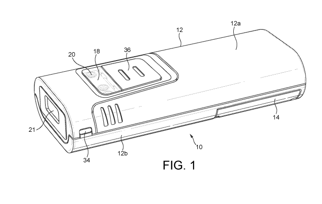
Figure 1 shows an embodiment of an authentication device 10 for authenticating
a
luminescent security mark (otherwise known as a "taggant"). The authentication
device
is a compact, pocket-sized device which may also be referred to as a fob
reader.
The authentication device 10 may be regarded as a portable, hand-held device
due to
5 its compact size and ergonomic shape, and by virtue of being battery-
powered.
With reference also to Figures 2 and 3, the authentication device 10 comprises
an
outer casing 12 which generally defines an elongate profile of substantially
obround
cross-section. The outer casing 12 is formed essentially of two sections, a
front (or
10 top) section 12a and a rear (or bottom) section 12b, which are connected
to one
another to encase the internal components of the authentication device 10, as
will be
described in more detail below.
The rear section 12b of the outer casing 12 comprises a battery compartment
cover 14
which provides access to an internal battery compartment (not shown). The
battery
compartment cover 14 therefore allows a battery of the device to be accessed
and
replaced.
As shown in Figure 2, the outer casing also defines an eye or through-hole 16.
The
eye 16 is defined by two cooperating through-holes formed at an upper end of
the front
and rear sections 12a, 12b of the outer casing 12. The eye 16 may be used to
connect
the authentication device 10 to a lanyard, such as a wrist or neck strap (not
shown),
using a cow hitch knot. The lanyard helps to prevent the authentication device
10 from
being dropped and also allows the authentication device to be kept in an
easily
accessible and convenient location.
The outer casing 12 further comprises an indicator window 18 formed in the
front
section 12a of the outer casing 12. The indicator window 18 is transparent or
translucent. The indicator window 18 is disposed over one or more indicator
lights 20,
such as light emitting diodes (LEDs), which allows the indicator lights 20 to
be viewed
by a user. As shown in Figure 1, the authentication device 10 may comprise
three
indicator lights 20, the function of which will be described in more detail
below. As
shown particularly in Figure 3, a cover member is disposed between the
indicator lights
20 and the indicator window 18. The cover member is provided with
complementary
apertures which are aligned with the indicator lights 20. The cover member
therefore
enables the indicator lights 20 to be viewed through the indicator window 18
via the
CA 02889653 2015-04-27
WO 2014/072707
PCT/GB2013/052908
6
apertures of the cover member but obscures the underlying internal circuitry
so that it
cannot be seen through the indicator window 18. Alternatively, the indicator
lights 20
may be mounted directly in the front section 12a of the outer casing 12 (using
a similar
arrangement to the cover member) without being covered by a window. The
authentication device 10 is also provided with a sample button 36 which, as
described
in detail below, can be depressed to commence an authentication process.
An end surface of the outer casing 12 is provided with an aperture within
which is
disposed a lens 21 for filtering ambient light and against which an optical
waveguide 22
abuts. This will be described in detail below.
The internal circuitry of the authentication device 10 will now be described
with
reference to Figure 4. The internal circuitry comprises a main printed circuit
board
(PCB) 24, the dimensions of which correspond substantially to that of the
outer casing
12. The main PCB 24 is provided with the necessary components for performing a
processing procedure. The main PCB 24 also forms a connection with a power
source
which, as described previously and shown in Figure 4, is preferably a battery
26.
An extension PCB 28 is connected to the main PCB 24. The extension PCB 28 is
located towards a front end of the main PCB 24. The extension PCB 28 extends
along
the width of the main PCB 24 and is oriented orthogonally with respect to the
main
PCB 24. The extension PCB 28 and the main PCB 24 are both physically and
electrically connected to one another. The dimensions of the extension PCB 28
correspond substantially to the cross-section of the outer casing 12 (taking
into account
the position of the main PCB 24).
The indicator lights 20 are provided on an upper surface of the extension PCB
28 with
their emitting surfaces oriented so as to be parallel with the main PCB 24.
The
extension PCB 28 therefore holds the emitting surfaces of the indicator lights
20
against the cover member described previously so that they can viewed through
the
indicator window 18.
A lower surface of the extension PCB 28 is provided with an illumination
source in the
form of a two LEDs 30. The LEDs 30 may be infra-red LEDs that emit infra-red
radiation having a wavelength of approximately 940 nm.
CA 02889653 2015-04-27
WO 201-1/072707
PCT/GB2013/052908
7
The illumination source preferably comprises two LEDs 30 as shown in Figure 4.
In
this embodiment the LEDs 30 are infrared LEDs that emit infrared light at a
wavelength
of around 940nm. The LEDs 30 are surface mount components and thus have a low-
profile. The LEDs 30 each have a substantially planar emitting surface which
is
coupled to an adjacent internal (with respect to the outer casing 12) surface
of the
optical waveguide 22. The internal surface of the optical waveguide 22 is also
substantially planar such that the LEDs 30 abut intimately with the optical
waveguide
22 across the emitting surfaces. The planar emitting surfaces of the LEDs 30
may be
connected to the internal surface of the optical waveguide 22 using an optical
glue to
improve coupling.
The LEDs 30 are oriented on the extension PCB 28 such that they are parallel
to one
another. In other words, the planar emitting surfaces of the LEDs 30 are
parallel with
the extension PCB 28 and each lie in a common plane. Accordingly, the LEDs 30
are
configured to emit excitation radiation in a common direction. Further, the
LEDs 30 are
arranged on the extension PCB 28 so that they are disposed side-by-side along
a
linear line.
The lower surface of the extension PCB 28 further comprises a radiation
detector in the
form of a photodetector 31 disposed between the two LEDs 30. The radiation
detector
31 is arranged to detect infra-red radiation emitted from a security mark.
Like the LEDs
30, the radiation detector 31 is also coupled to the internal surface of the
optical
waveguide 22. In this embodiment, the radiation detector 31 is a surface mount
radiation detector having a substantially planar receiving surface which abuts
the
internal surface of the optical waveguide 22. As for the LEDs 30, the planar
emitting
surface of the radiation detector 31 may be connected to the internal surface
of the
optical waveguide 22 using an optical glue to improve coupling.
The optical waveguide 22 is essentially a cuboid formed of a solid optical
material,
such as acrylic glass (e.g. ultra clear Perspex) having all sides highly
polished.
However, the optical waveguide may alternatively have a circular or other
suitable
cross-section. The optical waveguide 22 is configured to transmit light from
the internal
surface to an external (with respect to the outer casing 12) surface, and vice
versa.
The optical waveguide 22 is positioned relative to the LEDs 30 and the
radiation
detector 31 and configured so as to guide both excitation radiation emitted
from the
LEDs towards a security mark, and luminescent radiation emitted by the
security mark
CA 02889653 2015-04-27
WO 2014/072707
PCT/GB2013/052908
8
towards the radiation detector 31. For example, the optical waveguide 22 may
transmit
light between the internal and external surfaces via internal reflection.
If necessary, the side surfaces (i.e. the surfaces connecting the internal and
external
surfaces) of the optical waveguide 22 may be covered by a cladding material.
The
cladding material is selected so as to have a lower refractive index than that
of the
optical material. Consequently, light will be reflected at the interface
between the
optical material and the cladding material, thus preventing light from being
lost from the
side surfaces.
As described previously, an internal surface of the optical waveguide 22 is
coupled to
the illumination source (LEDs 30) and the radiation detector 31. The internal
surface of
the optical waveguide 22 is held in intimate contact with the LEDs 30 so as to
minimise
the light lost at the interface through reflection. The external surface of
the optical
waveguide 22 abuts the lens 21 which is received in an aperture provided at an
end
surface of the outer casing 12. Alternatively, the external surface of the
optical
waveguide 22 may be held against the end surface of the outer casing 12 such
that the
external surface is adjacent the aperture.
A visual security mark alignment guide 34 is provided on the outer casing 12
of the
authentication device 10. There are two pairs of alignment guides 34, a first
positioned
on the linear line along which the LEDs 30 are disposed, and a second
positioned
perpendicular to the first. The alignment guide 34 provides a visual
indication of the
position of the LEDs 30 beneath the optical waveguide 22. Accordingly, the
alignment
guide 34 allows a user to easily align the security mark with the light
emitted from the
optical waveguide 22. The alignment guide 34is preferably provided on the
outer
casing 12 so that it is visible when the end surface of the authentication
device 10 is
placed against a security mark. Alternatively or in addition, the alignment
guide 34 may
extend along the end surface of the authentication device 10.
The optical waveguide 22 is therefore able to transmit light (excitation
radiation)
generated by the illumination source from its internal surface to its external
surface and
out of the authentication device 10 through the lens 21. Similarly, the
optical
waveguide 22 is able to transmit light (luminescent radiation) generated
externally to
the authentication device 10 from its external surface to its internal surface
and to the
radiation detector 31.
CA 02889653 2015-04-27
WO 2014/072707
PCT/GB2013/052908
9
The operation of the authentication device 10 and an automated authentication
procedure will now be described in more detail.
In order to authenticate a luminescent security mark (or an article which may
or should
be provided with a security mark), the user places the end comprising the
optical
waveguide 22 of the authentication device 10 adjacent to a security mark to be
verified.
The security mark is aligned with the visual security mark alignment guide 34
which
ensures that the optical waveguide 22 is over the security mark. The
authentication
device 10 may be able to authenticate a security mark which is located a short
distance
(i.e. in the region of 0-10 centimetres) away from the external surface of the
optical
waveguide 22.
Once aligned, the user triggers an authentication process by depressing the
sample
button 36. This starts a short warm-up sequence in which all of the electronic
circuitry
is activated. Following the warm-up sequence, the LEDs 30 are activated so as
to
generate a pulse of infra-red excitation radiation. The excitation radiation
is transmitted
by the optical waveguide 22 from its internal surface to its external surface
where it is
received by the security mark. The excitation radiation causes the security
mark to
emit luminescent radiation which decays with time. The emitted luminescent
radiation
is transmitted by the optical waveguide 22 from its external surface to its
internal
surface where it is received by the radiation detector 31.
The decay constant of the luminescent radiation is characteristic of the
particular mark
and can therefore be used to authenticate the mark. In this particular
embodiment the
decay response is characterised by measuring two intensity values at
predetermined
time intervals based on the radiation received at the radiation detector 31
and taking a
ratio of the two intensity values. This ratio value can be compared with pre-
stored
reference values to determine if the mark is authentic.
In order to obtain accurate results, the mark is repeatedly illuminated and
sampled a
large number of times so as to obtain a set of ratio values. The set of ratio
values is
then averaged to give a sample. For example, 64 ratio values may be obtained
and
averaged. This process may be repeated a number of times (preferably in the
order of
7 or 8). Each of the samples (i.e. the average values) is then allocated into
one of a
plurality of buckets. Each of the buckets covers a predefined but configurable
range of
CA 02889653 2015-04-27
WO 2014/072707
PCT/GB2013/052908
values. The ranges of adjacent buckets need not be continuous. The ranges
defined
by each bucket may relate to a specific security mark or taggant material.
If a predefined number of samples fall within a single bucket, then the mark
is deemed
5 authentic. It may be necessary for the samples falling within that bucket
to have been
taken consecutively in order to gain a positive verification. On the other
hand, if there
are not sufficient samples in a single bucket, then the mark is not deemed to
be
authentic.
10 A positive and/or negative authentication may be signalled by the
indicator lights 20.
For example, a positive authentication may be signalled by a green LED,
whereas a
negative authentication may be signalled by a red LED. The authentication
device 10
may also comprise an audible indication or vibration that the security mark
has (or has
not) been successfully authenticated.
As described previously, the LEDs 30 are arranged parallel to one another such
that
they emit excitation radiation in a common direction. The optical waveguide 22
acts to
further collimate the excitation radiation through internal reflection within
the optical
waveguide 22. Consequently, the light emitted from the external surface of the
optical
waveguide 22 is substantially uniform. Accordingly, it is not necessary to
position the
security mark at a hot spot of the light in order to improve the accuracy of
the
authentication process. The authentication device of the present invention
thus
provides a more repeatable measurement which is less sensitive to measurement
conditions. This allows measurements to be taken more quickly without
sacrificing
accuracy. Further, the optical waveguide 22 allows surface mount LEDs to be
used as
the illumination source. This considerably reduces the size of the
authentication device
10.
Although the authentication device 10 has been described as being battery
powered, it
may also include an external power connector which allows the authentication
device
10 to be connected to a mains power supply. This may be particularly
beneficial where
the authentication device 10 is being used for a prolonged period in a
location where a
mains power source is available. The external power connector could also be
used to
recharge the battery of the authentication device, if appropriate.
CA 02889653 2015-04-27
WO 2014/072707
PCT/GB2013/052908
11
The authentication device may contain more than one radiation detector 31,
where
appropriate.
The authentication device 10 can be used in any orientation and thus the
relative
terms, such as upper and lower, used herein should not be considered
prescriptive of a
particular operative orientation.