Note: Descriptions are shown in the official language in which they were submitted.
CA 02889932 2015-04-29
WO 2014/067902 1 PCT/EP2013/072517
MEDIUM VOLTAGE CONNECTION
The invention relates to a medium voltage connection, comprising:
- a first conductor and a second conductor electrically attached to each
other;
- a first isolating layer arranged around the first conductor and a second
isolating layer
arranged around the second conductor, leaving an airgap between both isolating
layers;
- an isolating rubber sleeve arranged between the first isolating layer and
the second
isolating layer to fill the airgap between the two isolating layers.
Such medium voltage connections are known and are used in switchgear to
connect
for example inbound or outbound cables to the switchgear. These medium voltage
connections are also used to connect the busbars of adjacent panels of
switchgear.
In some applications of the medium voltage connections at least the first
conductor is
provided with a ground screen. Such a screen is for example used at busbar
connections or with current transformers, which are typically used to provide
a low
voltage signal for measuring the current in the first conductor. In this last
application,
it is necessary to have a grounding screen between the first conductor and the
coil
arranged around the conductor to prevent flash over to the low voltage side.
It is known to embed a grounding screen in the isolating layer around the
conductor.
In manufacturing, a perforated tube is positioned concentrically around the
conductor,
where after a resin is cast around the conductor and the screen. The
perforations
ensure that the resin can penetrate the screen.
It proves however that this manufacturing method results in a high number of
rejected
products. This is the result of misaligned screens, deformed screens and air
pockets in
the resin.
CA 02889932 2015-04-29
WO 2014/067902 2 PCT/EP2013/072517
Another disadvantage of the known screens, is that a high field density is
present
around the edge of the screens. Because the screen is embedded in isolating
material,
the field density will extend into the air surrounding the medium voltage
connection,
which is undesired, especially with low voltages components near the medium
voltage
connection. This could lead to undesired electrical discharges.
Yet another disadvantage of the known medium voltage connection, is that when
connecting for example a cable to the first conductor with embedded screen in
the
isolating layer, the medium voltage connection is subjected to substantial
mechanical
stresses. These mechanical stresses are caused by the weight of the cable and
by the
expanding and shrinking of the isolating material due to heating and cooling
of the
connection. In time, this results in cracks in the isolating layer.
It is an object of the invention to reduce or even remove the above mentioned
disadvantages.
This object is achieved with a medium voltage connection according to the
invention,
which is characterized in that a conducting layer is arranged on the first
isolating
layer; and in that the rubber sleeve is provided with a conducting portion,
which
overlaps with the conducting layer.
By providing a conducting layer on the isolating layer, it is ensured that the
grounding
screen provided by the conducting layer is always correctly positioned. It is
no longer
necessary to already position the screen before casting the isolating layer,
but with the
invention the isolating layer can be cast first and afterwards, the conducting
layer can
be arranged. This substantially reduces the number of rejects during
manufacturing, as
positioning of the screen will always be correct.
The conducting portion of the rubber sleeve ensures that the end of the screen
is
extended into the airgap between the two isolating layers. The high field
concentration typically present at the edge of the screen is in this way moved
to a
position well enveloped by isolating material.
CA 02889932 2015-04-29
WO 2014/067902 3 PCT/EP2013/072517
An additional advantage of arranging the conducting layer on the isolating
layer of the
conductor, is that with the same outer dimensions a thicker layer of
insulating material
is present between the screen and the conductor. This substantially increases
the
dielectric robustness.
As the screen is arranged on the outside and no longer embedded in the
isolation
layer, as with the prior art, the mechanical stresses have less influence,
resulting in a
better durability.
In a preferred embodiment of the medium voltage connection according to the
invention, the transition between the conducting portion and isolating portion
of the
rubber sleeve is positioned between the first and second isolating layers.
The rubber sleeve can be composed out of two separate materials, one isolating
portion and one conducting portion. The conducting portion is brought in
electrical
contact with the conducting layer. In this way, the electrical screen is
extended and
the edge of the screen is displaced to in between the isolating layers. Any
high
electrical field concentrations will be kept with the isolating material.
In another embodiment of the medium voltage connection according to the
invention
the second isolating layer partially envelopes the rubber sleeve and the first
isolating
layer. This further increases the thickness of isolating material over the
extended edge
of the screen.
Preferably the conducting portion of the rubber sleeve is carbon black filled.
Carbon
black provides electric conducting properties and can be reliably processed in
the
manufacturing of the rubber sleeve.
In yet another preferred embodiment of the medium voltage connection according
to
the invention, a secondary coil is arranged around the first conductor for
measuring
the current in the first conductor.
CA 02889932 2015-04-29
WO 2014/067902 4 PCT/EP2013/072517
The invention is typically, but not exclusively, suited for use in current
transformers,
in which it is mandatory that the secondary coil is shielded by a grounding
screen
from the medium voltage conductor.
-- Preferably, the conducting layer is a conducting paint layer. Such a
conducting paint
layer is easily applied on the surface of the isolating layer surrounding the
conductor.
These and other features of the invention, will be elucidated in conjunction
with the
accompanying drawings.
-- Figure 1 shows a cross sectional view of an embodiment of a medium voltage
connection according to the prior art.
Figure 2 shows a cross sectional view of an embodiment of a medium voltage
connection according to the invention.
Figure 1 shows an embodiment 1 of a medium voltage connection according to the
prior art. This connection 1 has a first conductor 2 and a second conductor 3,
which
can be bolted together by the threaded holes 4, 5.
-- The first conductor 3 is provided with a first isolating layer 6. Within
the isolating
layer 6, a metal screen 7 is embedded. The edge 8 of the metal screen 7 is
bent back to
reduce the electrical field concentration.
The second conductor 3 is also provided with an insulating layer 9, which has
-- extending edges 10 enveloping the end of the conductor 2.
A rubber sleeve 11 is arranged in between the first isolating layer 6 and the
isolating
layer 9, 10 to fill the gap.
-- Because the edge 8 of the screen 7 is at a distance from the rubber sleeve
11 and the
extending edges 10, the electrical field surrounding this edge 8 easily
extends into the
air around the medium voltage connection 1.
CA 02889932 2015-04-29
WO 2014/067902 5
PCT/EP2013/072517
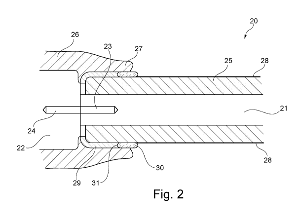
Figure 2 shows a cross sectional view of an embodiment 20 of the invention.
The
medium voltage connection 20 has a first conductor 21 and a second conductor
22,
which can be bolted together via the threaded holes 23, 24.
The first conductor 21 is provided with an isolating layer 25, while the
second
conductor 22 is also provided with an isolating layer 26 having extending
edges 27 to
envelope the end of the first conductor 21.
The outer surface of the first isolating layer 25 is provided with a
conducting coating
28 of for example conducting paint. This conduction coating 28 provides a
grounding
screen.
A rubber sleeve 29, 30 is arranged between the first isolating layer 25 and
the second
isolating layer 26. This rubber sleeve 29, 30 has a isolating portion 29 and a
conducting portion 30.
This conducting portion 30 is in contact with the conducting coating 28, such
that the
edge 31 of the screen 28 is formed by the interface between the conducting
portion 30
and the isolating portion 29.
As a result, the edge 31 of the screen is embedded between isolating edge 27
and the
isolating layer 25.