Note: Descriptions are shown in the official language in which they were submitted.
CA 02889975 2015-04-30
WO 2014/070534 PCT/US2013/066266
INTEGRATED BONDLINE SPACERS FOR WAFER LEVEL PACKAGED CIRCUIT
DEVICES
BACKGROUND
[0001] The present disclosure relates generally to semiconductor device
manufacturing and, more particularly, to bond gap control structures (BGCS)
for wafer level
packaged optical microelectromechanical systems (MEMS) devices.
[0002] Micro electromechanical systems (MEMS) are integrated micro devices or
systems combining electrical and mechanical components. MEMS devices may be
fabricated
using, for example, standard integrated circuit batch processing techniques.
Exemplary
applications for MEMS devices include sensing, controlling, and actuating on
the micro
scale. Such MEMS devices may function individually or in arrays to generate
effects on a
macro scale.
[0003] Many MEMS devices require a vacuum environment in order to attain
maximum performance. The vacuum package also provides protection and an
optimal
operating environment for the MEMS device. Specific examples of these MEMS
devices
include infrared MEMS such as bolometers, and certain inertial MEMS such as
gyros and
accelerometers. Previously, MEMS devices have been individually packaged in
vacuum
compatible packages after fabrication and dicing of the MEMS device. Often,
however, the
cost of packaging MEMS devices in traditional metal or ceramic packages may be
on the
order of about 10 to 100 times the device fabrication cost. This especially
true if a vacuum is
required in the package. These high packaging costs therefore make it
difficult to develop
commercially viable vacuum packaged MEMS devices. In addition, MEMS devices
are
fragile especially after dicing. Care must be taken in handling these devices,
and traditional
integrated circuit fabrication machinery cannot adequately handle and protect
MEMS
devices. Thus, special handling techniques have also been developed to protect
the MEMS
devices until vacuum packaging has been completed. These special handling
procedures also
add additional cost to the production of MEMS devices.
[0004] Wafer Level Packaging (WLP) was developed to address the high cost of
packaging of MEMS by eliminating the traditional packages. In the WLP process,
two
semiconductor wafers may be bonded together using a joining material to yield
bonded
wafers. For example, a device wafer may be bonded to a lid wafer using an
adhesive or
solder to form a packaged MEMS device. Certain applications may require that
the joining
material form a substantially uniform bond line. In certain situations,
substrates (such as
1
CA 02889975 2015-04-30
WO 2014/070534 PCT/US2013/066266
silicon wafers) may be bonded together using a joining material. After
bonding, the joining
material forms a bond line in between the substrates. However, the uniformity
of the bond
line may be affected by the flatness of the substrates and the uniformity of
the bond force
used to bond the wafers. The uniformity of the bond line may be controlled by
placing
spacers at certain intervals across the surface of one or both substrates.
However, adding the
spacers usually requires adding process steps to the fabrication process.
SUMMARY
[0005] In an exemplary embodiment, a method of forming a wafer level packaged
circuit device includes forming a device wafer, the device wafer including a
first group of one
or more material layers left remaining in a first region of a substrate of the
device wafer; and
forming a cap wafer configured to be attached to the device wafer, the cap
wafer including a
second group of one or more material layers left remaining in a second region
of a substrate
of the cap wafer; wherein a combined thickness of the first and second groups
of one or more
material layers defines an integrated bond gap control structure upon bonding
of the device
wafer and the cap wafer.
[0006] In another embodiment, a method of forming a wafer level packaged
circuit
device includes forming a device wafer, the device wafer including a polyimide
layer formed
in a first region of a substrate of the device wafer, and a first solder metal
stack layer formed
on the polyimide layer, wherein the polyimide layer is a same polyimide layer
that is also
used in the formation of microelectromechanical systems (MEMS) devices of an
integrated
circuit on the device wafer, and the first solder metal stack layer is also a
same first solder
metal stack layer used to form a sealing ring for the device wafer; forming a
cap wafer, the
cap wafer including an antireflective coating layer formed in a second region
of a substrate of
the cap wafer, and a second solder metal stack layer formed on the
antireflective coating
layer, wherein the antireflective coating layer is a same antireflective
coating layer that is also
formed on a cavity portion of the cap wafer, and the second solder metal stack
layer is also a
same second solder metal stack layer used to form a sealing ring for the cap
wafer; and
bonding the cap wafer to the device wafer, thereby defining an integrated bond
gap control
structure comprising the polyimide layer, the first solder metal stack layer,
the second solder
metal stack layer, and the antireflective coating layer. If a getter is used
in the package, it
may also be included in the BGCS structure described above.
[0007] In another embodiment, a wafer level packaged circuit device includes a
device wafer bonded to a cap wafer. The device wafer includes a polyimide
layer formed in a
2
CA 02889975 2015-04-30
WO 2014/070534 PCT/US2013/066266
first region of a substrate of the device wafer, and a first solder metal
stack layer formed on
the polyimide layer, wherein the polyimide layer is a same polyimide layer
that is also used
in the formation of an integrated circuit on the device wafer, and the first
solder metal stack
layer is also a same first solder metal stack layer used to form a sealing
ring for the device
wafer. The cap wafer includes an antireflective coating layer formed in a
second region of a
substrate of the cap wafer, and a second solder metal stack layer formed on
the antireflective
coating layer, wherein the antireflective coating layer is a same
antireflective coating layer
that is also formed on a cavity portion of the cap wafer, and the second
solder metal stack
layer is also a same second solder metal stack layer used to form a sealing
ring for the cap
wafer; and an integrated bond gap control structure (BGCS) disposed between
the device
wafer and the cap wafer, the integrated BGCS comprising the polyimide layer,
the first solder
metal stack layer, the second solder metal stack layer, and the antireflective
coating layer.
[0008] In another embodiment, a method of forming a wafer level packaged
circuit
device includes forming a device wafer; forming a cap wafer; forming, on
either the cap
wafer or the device wafer, a bond gap control structure comprising one or more
material
layers used in the formation of either the cap wafer or the device wafer, and
left remaining in
a region of a substrate of either the cap wafer or the device wafer; and
bonding the cap wafer
to the device wafer.
BRIEF DESCRIPTION OF THE DRAWINGS
[0009] For a more complete understanding of this disclosure, reference is now
made
to the following brief description, taken in connection with the accompanying
drawings and
detailed description, wherein like reference numerals represent like parts:
[0010] Figure 1(a) illustrates a top down acoustic image of a bonded pair of
wafers
without a BGCS showing the results of nonuniformity of the bond line;
[0011] Figure 1(b) is a side cross sectional view of a bonded pair of wafers
without a
BGCS showing nonuniformity of the bond line, and causing solder to flow
outside a specified
bond region;
[0012] Figure 2 is a top view of a patterned side of an exemplary cap wafer
that may
be used in accordance with the teachings herein;
[0013] Figure 3 is an enlarged top view of a patterned side of an exemplary
cap wafer
that may be used in accordance with the teachings herein;
3
CA 02889975 2015-04-30
WO 2014/070534 PCT/US2013/066266
[0014] Figure 4 is a side cross sectional view of a portion of a device wafer
to be
bonded to a corresponding portion of a cap wafer that results in the formation
of integrated
BGCSs, in accordance with an exemplary embodiment;
[0015] Figure 5 is a side cross sectional view illustrating bonding of the
device and
cap wafers of Figure 4;
[0016] Figure 6 is a side cross sectional view of a portion of a device wafer
to be
bonded to a corresponding portion of a cap wafer that results in the formation
of integrated
BGCSs, in accordance with another exemplary embodiment;
[0017] Figure 7 is a side cross sectional view illustrating bonding of the
device and
cap wafers of Figure 6;
[0018] Figure 8 is a top view illustrating the placement of a vacuum getter
layer atop
the solder base metal layer of the cap wafer in the embodiment of Figures 6
and 7;
[0019] Figure 9 is a cross sectional, perspective view illustrating the
placement of the
vacuum getter layer atop the solder metal layer of Figure 8;
[0020] Figure 10 is a side cross sectional view of a portion of a device wafer
to be
bonded to a corresponding portion of a cap wafer that results in the formation
of integrated
BGCSs, in accordance with another exemplary embodiment;
[0021] Figure 11 is a side cross sectional view illustrating bonding of the
device and
cap wafers of Figure 10;
[0022] Figure 12 is a side cross sectional view of a portion of a device wafer
to be
bonded to a corresponding portion of a cap wafer that results in the formation
of integrated
BGCSs, in accordance with another exemplary embodiment; and
[0023] Figure 13 is a side cross sectional view illustrating bonding of the
device and
cap wafers of Figure 12.
DETAILED DESCRIPTION
[0024] It will be appreciated that for simplicity and clarity of illustration,
where
appropriate, reference numerals have been repeated among the different figures
to indicate
corresponding or analogous elements. In addition, numerous specific details
are set forth in
order to provide a thorough understanding of the embodiments described herein.
However, it
will be understood by those of ordinary skill in the art that the embodiments
described herein
can be practiced without these specific details. In other instances, methods,
procedures and
components have not been described in detail so as not to obscure the related
relevant
4
CA 02889975 2015-04-30
WO 2014/070534 PCT/US2013/066266
feature(s) being described. Also, the description is not to be considered as
limiting the scope
of the embodiments described herein.
[0025] As indicated above, infrared MEMS devices and certain other inertial
MEMS
devices require a vacuum environment to attain maximum performance. For
example,
infrared microbolometers require an operating pressure of less than 10
millitorr (mT) to
minimize thermal transfer from the detector elements to the substrate and
package walls.
Thus, vacuum compatible materials processes and equipment must be used.
Infrared devices
also require an optically transparent cover. These packaging requirements
translate to high
labor and capital expense and present a significant cost barrier to
commercially viable MEMS
devices. Traditional MEMS device packaging costs can be ten to one hundred
times the basic
device fabrication cost even in reasonably high volume.
[0026] A solution to high packaging costs is to eliminate the traditional
individual
vacuum packaging of a completed die. More specifically, this is achieved by
moving the
packaging step into the wafer fabrication area. A cap wafer is aligned and
mounted to the
device wafer with an annular seal ring of solder, or other sealing material,
forming an
enclosed cell at each die location. This cap attachment process is completed
in a vacuum
environment, leaving each MEMS device in a vacuum cell. Interconnects are
brought out
under the solder seal ring and are isolated by a dielectric layer.
[0027] Figure 1(a) illustrates an image of a bonded pair of wafers 100. When
bonding two wafers together, regardless of whether the joining material is
solder, adhesive, or
some other intermediates, the flatness of the substrates and the amount and
uniformity of
bond force largely determine the bond line geometries in terms of gap
(thickness) and width.
As illustrated in the circled regions 102, the bonded wafer pair 100 exhibits
bond width and
gap uniformity issues in the absence of a bond gap control structure or spacer
(BGCS). As
further depicted in the side cross sectional view of Figure 1(b), the bonded
pair of wafers 104,
106, without a BGCS further results in causing solder 108 to flow outside a
specified bond
region.
[0028] A BGCS may serve as a mechanical stop that controls the thickness of a
bond
line between two surfaces joined by solder, adhesive, or other joining
material, and also
prevents the joining material from spreading in an undesired manner. In
certain
embodiments, a BGCS may be disposable (i.e., may be removed during wafer
dicing). If the
BGCS is formed from materials that are not otherwise used in the formation of
either the cap
wafer or the device wafer (e.g., a polyimide or other material), then this
results in additional
processing steps. Any additional process or processes can in turn increase the
risk of adding
CA 02889975 2015-04-30
WO 2014/070534 PCT/US2013/066266
contamination in the form of particles or chemical residues to the optical
window surfaces
that are difficult to clean.
[0029] Accordingly, in the present embodiments, existing layers used in the
formation
of an integrated circuit wafer (e.g., an infrared (IR) detector) and/or a cap
wafer can now also
be advantageously used in the formation of bond gap spacers. Rather than
forming additional
layers on completed device and cap wafers, the package fabrication process may
easily be
modified to leave small regions of these layers to form spacers of the
materials that are
already integral to the process. In so doing, the present embodiments
eliminate a separate
spacer forming step in the cap wafer fabrication, which in turn involves
spraying or spinning
a separate layer of polyimide material (for example) on the wafer, photo-
patterning the
spacers, baking the material to harden it, and removing all residual traces
from the optical
surfaces. Further, this approach also eliminates a possible need for capital
equipment for the
spray deposition of the polyimide, as it is often not compatible with
photoresist dispensing
equipment. Still another advantage is the simplification of the packaging
process and
enhancement of product yield by reducing risk of leaving residue on optical
surfaces.
Residue and particles are a prime caused of rejection for optical failures,
and organic residue
in the package is a prime cause of loss due to poor vacuum and shortened
product life.
[0030] Referring now to Figure 2, there is shown a top view of a patterned
side of an
exemplary cap wafer 200 that may be used in accordance with the teachings
herein. The cap
wafer 200 may, in one embodiment include a silicon substrate 202, although any
suitable
wafer substrate material may be used. The cap wafer 200 includes a plurality
of cap sealing
rings 204 corresponding in number to device sealing rings on an integrated
circuit device
wafer (not shown in Figure 2). Each of the cap sealing rings 204 corresponds
to a device
sealing ring so that the cap wafer 200 mates with a device wafer. Cavities 206
and bonding
pad channels 208 are formed in the cap wafer 200 using an appropriate process
such as wet or
dry etching.
[0031] The cavities 206 provide an increased volume for a vacuum packaged MEMS
device (not shown in Figure 2), which in turn provides for a lower vacuum
pressure level
within the vacuum cell. The bonding pad channels 208 may be used to provide
clearance
over bonding pads (not shown in Figure 2) so that a dicing saw, etching
process, or other
suitable process may be used in a later step to open the lid wafer to expose
the bonding pads
for device testing before dicing of the wafer.
[0032] As further depicted in Figure 2, the cap wafer 200 includes a plurality
of bond
gap control structures 210 adjacent the outer perimeter of the cap sealing
rings 204. Again,
6
CA 02889975 2015-04-30
WO 2014/070534 PCT/US2013/066266
the bond gap control structures 210 serve as a mechanical stop that controls
the thickness of a
bond line between two joined surfaces. In the embodiment illustrated, the bond
gap control
structures 210 are schematically depicted as single structures disposed in a y-
axis direction
with respect to Figure 2, whereas the bonding pad channels 208 are generally
disposed in an
x-axis direction with respect to Figure 2. However, other arrangements are
also possible with
respect to the cap wafer 200.
[0033] For example, Figure 3 is an enlarged top view of a patterned side of an
exemplary cap wafer 300 that may also be used in accordance with the teachings
herein. For
ease of illustration, like reference numbers with respect to Figure 2 are used
in Figure 3. As
is shown in the more detailed view of Figure 3, the substrate 202 has saw
lines 302 depicted
approximately in the center of scribe regions 304 where the substrate 202 is
to be cut. In this
embodiment, a plurality of BGCSs 210 are disposed within the scribe regions
304, in both the
x-axis and y-axis directions to operate as a mechanical stop that controls the
geometry of a
bond line of a cap sealing ring 204. In an exemplary embodiment, the BGCS may
only need
to be disposed in either the x-axis or y-axis directions. The geometry of a
bond line includes
both gap thickness and width. The gap refers to the gap between bonded
substrates, wherein
the gap thickness is measured in a direction that is perpendicular to the flat
surface of the
substrate 202. The width is measured along the flat surface of substrate 202.
A BGCS 210
may have any suitable size and shape. For example, each BGCS 210 may have a
width in
any of the following ranges 1 to 10, 10 to 50, 50 to 100, or over 100 microns
(um), a length in
any of the following ranges 50 to 100, 100 to 200, or over 200 um, and a
thickness in any of
the following ranges 1 to 5, 5 to 10, 10 to 20, or over 20.
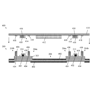
[0034] Referring now to Figure 4, there is shown a side cross sectional view
of a
portion of a device wafer 400 to be bonded to a corresponding portion of a cap
wafer 200.
Again, for ease of illustration, like reference numbers with respect to the
cap wafers of
Figures 2 and 3 are used in Figure 4. As depicted in Figure 4, the cap wafer
200 is shown in
a bottom, cavity-up orientation and includes the substrate 202, etched out
cavity 206, and a
cap sealing ring 204a that surrounds the cavity 206. Adjacent sealing rings
204b are also
shown for adjacent cavities on the cap wafer 202 for illustrative purposes. A
cap wafer
portion of each BGCS 210 is also illustrated on the cap wafer 200 in Figure 4.
[0035] As indicated above, in contrast to using special materials to form
BGCSs, the
BGCSs are instead formed using existing materials for both the cap wafer 200
and the device
wafer 400. In the case of the cap wafer 200, a first layer for the BGCS 210
may include an
antireflective (AR) coating layer 402 also formed on the thinned portions of
the substrate 202
7
CA 02889975 2015-04-30
WO 2014/070534 PCT/US2013/066266
(i.e., corresponding to locations of the cavities 206 that will cover the
corresponding MEMS
devices on the device wafer 400), in accordance with the fabrication of
infrared detectors or
other such optical devices. In an exemplary embodiment, the AR portion of the
BGCS 210
may have a thickness on the order of about 5.5 [tm to about 8.0 [tm, and more
specifically
about 7.0 lam. In order to form the AR coating layer 402 at the BGCS
locations, in addition
to the existing locations on the cap wafer, the applicable patterning mask(s)
are modified so
that the AR material remains in the BGCS locations.
[0036] In addition, a second layer for the BGCS 210 may include a solder base
metal
stack layer 404 that is also used as a solder base for the sealing rings 204a,
204b. The solder
metal stack layer may include, for example, a layer of titanium (Ti), followed
by a layer of
nickel (Ni), and followed by a layer of gold (Au). Other metals, however, may
also be used.
The combined metal stack layer 404 may have an exemplary thickness on the
order of about
0.4 [tm to about 0.8 [tm, and more specifically about 0.6 lam. The formation
of the cap wafer
is completed with the addition of an appropriate solder metal layer 406 atop
the metal stack
layer 404 of the sealing rings 204a, 204b. If a sealing method other than heat
activated solder
is used, solder metal layer 406 is replaced by a material selected to obtain a
vacuum tight
seal. The solder metal layer 406 may be deposited through traditional
integrated circuit
fabrication techniques or other suitable deposition processes including, but
not limited to,
electroplating, electroless plating, and vacuum deposition.
[0037] Turning now to the device wafer 400, a substrate wafer 410 (e.g.,
silicon) has
a plurality of IC devices 412 formed thereon. The IC devices 412 may be MEMS
devices
such as a bolometer, for example, formed using traditional methods of
integrated circuit
fabrication. Although the present embodiment is discussed in terms of vacuum
packaging
for MEMS devices, the principles disclosed herein may be applied to vacuum
packaging of
any integrated circuit device, or similar device, formed on a substrate
material and contained
within a vacuum package. Each IC device 412 is configured to be aligned with a
corresponding cavity 206 on the cap wafer 200. As is the case with the cap
wafer 200, the
device wafer 400 may be formed with one or more materials that match up with
materials on
the cap wafer 200 to formed integrated BGCSs. In Figure 4, a device wafer
portion of each
BGCS is indicated at 414. That is, the device wafer portion 414 of a BGCS and
the cap
wafer portion 210 of a BGCS are mated to form an integrated BGCS, as shown
hereinafter.
[0038] With respect to the device wafer 400, a first layer for the device
wafer portion
414 of a BGCS may include a sacrificial polyimide layer 416 that is used to
thermally isolate
the IC device 412 (e.g., bolometer) from the substrate 410. In this sense, the
polyimide layer
8
CA 02889975 2015-04-30
WO 2014/070534 PCT/US2013/066266
416 is not sacrificial in the BGCS regions, in that that layer patterning is
adjusted such that
the polyimide remains to contribute to the overall BGCS thickness. In an
exemplary
embodiment, the polyimide layer 416 may have a thickness on the order of about
1.8 [tm to
about 2.0 pm.
[0039] As is the also case with the cap wafer 200, the device wafer 400 is
provided
with a solder base metal stack layer 418 that is used as a solder base to mate
with the solder
metal 406 atop the metal stack layer 404 of the sealing rings 204a, 204b. The
solder metal
stack layer 418 may also include a Ti/Ni/Au stack similar to stack 404, and at
a substantially
same thickness. In addition to serving as a solder base for sealing rings on
the device wafer,
the metal stack layer 418 may also serve as a second layer for the device
wafer portion 414 of
a BGCS. As particularly illustrated in Figure 4, patterning of the metal stack
layer 418 is
such that it covers not only the top surface of the polyimide layer 416, but
also the sidewall
surfaces thereof
[0040] With both the cap wafer 200 and device wafer 400 configured as depicted
in
Figure 4, the arrangement is ready for final assembly. To prepare the
assembly, the cap
wafer 200 may be placed in an assembly holder (not shown) with the solder
layer 406 facing
up. The device wafer 400 is aligned over the cap wafer 200 such that the metal
stack layers
418 (i.e., not the metal stack layers 418 that are part of the integrated
BGCS) are aligned over
the corresponding cap wafer sealing rings 204a, 204b.
[0041] Figure 5 depicts the joining of the cap wafer 200 with the device wafer
400 to
form an assembly 500. As can be seen, an integrated BGCS indicated at the
circled region
502 is defined by the combined material stack that includes the AR and solder
metal layer
402, 404, respectively from the cap wafer 200 and the solder metal layer and
polyimide
layers 418, 416, respectively, from the device wafer 400. The integrated
BGCSs, like
previous spacers, allow for good solder bond width and gap uniformity
characteristics for the
now-formed bond lines 504 in Figure 5, but without the need to form the BGCSs
using
additional materials not otherwise used in forming either the cap wafer 200 or
the device
wafer 400. In total, the bond lines may have an exemplary thickness on the
order of about 10
pm as result of the combined thicknesses of the AR, polyimide and metal layers
left in the
scribe regions of the cap and device wafers.
[0042] After any appropriate testing of the MEMS devices 12, the assembly 500
is
diced by sawing along, for example, a saw line 302 such as shown in Figure 3,
which may or
may not result in the removal of the integrated BGCS shown at 502 in Figure 5.
The dicing
of the assembly 500 may be accomplished by using traditional methods of dicing
9
CA 02889975 2015-04-30
WO 2014/070534 PCT/US2013/066266
semiconductor wafers with completed integrated circuits. By vacuum packaging
MEMS
devices 412 at the wafer level, traditional methods of handling integrated
circuit devices may
be used since the vacuum package provides protection to the delicate MEMS
device 412. A
completed die representing a vacuum packaged MEMS device 412 may be mounted by
chip-
on-board methods or injection molded into a plastic package (not shown). In
addition, a
completed die may be placed in a non-vacuum package with other components (not
shown).
[0043] Although the integrated BGCSs 502 in Figure 5 is shown disposed in or
proximate to a scribe region in between adjacent bond lines 504, it is also
contemplated that
the BGCSs 502 may also be positioned in additional locations. For example, the
BGCS
materials from the cap wafer 200 and device wafer 400 could be patterned such
that one or
more BGCSs 502 reside within the confines of the sealed cavity, such as at
location 506 for
example. In this case, the BGCS 502 would remain as part of the completed
product, after
dicing.
[0044] Referring now to Figure 6, there is shown a side cross sectional view
of a
portion of a device wafer 400 to be bonded to a corresponding portion of a cap
wafer 200 that
results in the formation of integrated BGCSs, in accordance with another
exemplary
embodiment. In this embodiment, an additional layer used in the processing of
the cap wafer
is also intentionally left in the scribe region of the substrate 202 in order
to contribute to the
overall thickness of the BGCS. More specifically, the cap wafer 200 includes a
vacuum
getter layer 602 initially formed on the inside surfaces of the cap substrate
202 over the AR
layer, corresponding to the etched cavity regions 206. Generally, a getter is
a deposit of
reactive material that is placed inside a vacuum system, for the purpose of
completing and
maintaining the vacuum. When gas molecules strike the getter material, the
molecules
combine with the getter chemically or by adsorption, removing small amounts of
gas from
the evacuated space. The getter layer 602 may include one or more layers of
elements such
as titanium, zirconium, iron, and vanadium, to name a few examples.
[0045] As further seen in Figure 6, the getter layer 602 is left remaining
atop the AR
and solder base metal layers 402, 404, respectively, to become a part of the
cap wafer portion
of each BGCS 210. In the bonded view of Figure 7, the assembly 700 includes
integrated
BGCSs, indicated by the dashed circled region 702. In an exemplary embodiment,
the getter
layer 602 may have a thickness on the order of about 0.3 [tm to about 2.0 um,
and more
specifically about 0.9 pm. As such, the embodiment of Figures 6 and 7, which
uses the
additional getter layer 602 in forming a BGCS, may provide for an additional
bond line
thickness of about 1.0 [tm or more with respect to the embodiment of Figures 4
and 5.
CA 02889975 2015-04-30
WO 2014/070534 PCT/US2013/066266
[0046] In order to achieve a desired plateau width for the portions of the
getter layer
602 that become a part of the BGCSs, an allowance may be made for shadowing of
the getter
deposition mask, as more particularly illustrated in Figures 8 and 9. In the
top view of Figure
8, reference number 802 depicts a width of a saw lane on the scribe region of
the cap wafer
substrate. The saw lane 802 may be on the order of about 480 lam. Region 804
represents the
solder metal stack portion of the BGCS that covers the top and sidewall
surfaces of the AR
layer (not shown in Figure 8). Region 806 represents the getter layer portion
of the BGCS
that overlaps the top surface or plateau of the solder base metal, which is
depicted by the
dashed line 808. In an embodiment, an exemplary width 810 of a shadowed edge
overlap of
the getter layer is on the order of about 40 lam.
[0047] Figure 9 is a cross sectional, perspective view illustrating the
placement of the
vacuum getter layer 806 atop the solder metal layer stack 804 of Figure 8. In
this view, the
AR layer depicted by region 902 is shown. The dashed lines 904 represent
regions of a getter
shadow mask, wherein a spacing 906 between the regions (i.e., the shadow mask
opening
width) represents the plateau width of the top of the solder metal stack 804
plus the shadowed
edge width 810.
[0048] In the embodiments described above, the BGCSs are formed using existing
materials for both the cap wafer 200 and the device wafer 400. However, it is
also
contemplated that the BGCS material could be formed from existing layers on
either the cap
wafer 200 alone or on the wafer layer 400 alone. In such a case, the overall
thickness of the
BGCSs may be reduced and/or in the alternative, the existing layers used to
form the cap
wafer 200 or the device wafer 400 may be formed at a greater initial thickness
so as to
compensate for the BGCS material being formed on only one of the two wafers.
[0049] By way of example, Figure 10 is a side cross sectional view of a
portion of a
device wafer 400 to be bonded to a corresponding portion of a cap wafer 200
that results in
the formation of integrated BGCSs, in accordance with another exemplary
embodiment. In
this embodiment, the BCGS layer(s) are formed only on the cap wafer 200. Here,
the layer(s)
are generally denoted at 1000, and may include one or more of the specific
layers previously
described as being formed on the cap wafer 200 such as, for example, AR
layers, solder base
metal stack layers, and getter layers. In the bonded view of Figure 11, the
BCGS layer(s)
1000 serve as the entire integrated BGCSs for the assembly 1100. Again, as
with the
previous embodiments, the integrated BGCSs 1000 may be located elsewhere
besides the
scribe regions.
11
CA 02889975 2015-04-30
WO 2014/070534 PCT/US2013/066266
[0050] Conversely, Figure 12 is a side cross sectional view of a portion of a
device
wafer 400 to be bonded to a corresponding portion of a cap wafer 200 that
results in the
formation of integrated BGCSs, in accordance with another exemplary
embodiment. In this
embodiment, the BCGS layer(s) are formed only on the device wafer 400. The
BGCS
layer(s) are generally denoted at 1200, and may include one or more of the
specific layers
previously described as being formed on the cap wafer 400 such as, for
example, solder base
metal stack layers and polyimide layers. In the bonded view of Figure 13, the
BCGS layer(s)
1200 serve as the entire integrated BGCSs for the assembly 1300.
[0051] As will thus be appreciated, among the technical benefits of the above
described embodiments is the elimination of added processing steps to
fabricate bond gap
control spacers from materials that are not used in the preparation of device
or cap wafer
structures. Fewer processing steps in turn results in cost reduction and less
chance for yield
loss. Rather, the BGCS material is advantageous taken from existing layers
formed on the
cap and/or device wafers that would ordinarily be removed from (or not
initially formed in)
the scribe regions of the wafers. Such exemplary materials include, but are
not necessarily
limited to, AR coatings, solder base metals, polyimides and vacuum getter
layers.
[0052] While the disclosure has been described with reference to a preferred
embodiment or embodiments, it will be understood by those skilled in the art
that various
changes may be made and equivalents may be substituted for elements thereof
without
departing from the scope of the disclosure. In addition, many modifications
may be made to
adapt a particular situation or material to the teachings of the disclosure
without departing
from the essential scope thereof. Therefore, it is intended that the
disclosure not be limited to
the particular embodiment disclosed as the best mode contemplated for carrying
out this
disclosure, but that the disclosure will include all embodiments falling
within the scope of the
appended claims.
12