Note: Descriptions are shown in the official language in which they were submitted.
CA 02890298 2015-04-07
WO 2014/058472
PCT/US2013/032584
CLOSED LOOP CONTROL TECHNIQUES FOR DISPLACEMENT SENSORS WITH
OPTICAL READOUT
CROSS REFERENCE TO RELATED APPLICATIONS
The current application claims the benefit of U.S. Provisional Patent No.
61/721,903, filed
November 2, 2012, and U.S. Provisional Patent No. 61/712,652, filed October
11, 2012 the
entire contents of each of which are incorporated herein by reference.
The current application is also related to U.S. Patent Publication Number
2011/0194711
published August 11, 2011, U.S. Patent Publication Number 2011/0194857
published August 11,
2011, U.S. Patent Number 7,116,430 granted October 3, 2006, U.S. Patent Number
7,485,847
granted February 3, 2009, U.S. Patent Number 6,643,025 granted November 4,
2003, and U.S.
Patent Number 6,753,969 granted June 22, 2004 the entire contents of each of
which are
incorporated herein by reference.
BACKGROUND
The following section is presented for informational purposes only. The
inclusion of material in
this section should not be considered to be an admission that such material is
prior art to the
present application.
Some embodiments disclosed herein are directed to systems, devices, and
methods for seismic
sensing, e.g., suitable for use as a geophone. A geophone is a device that
converts ground
movement (displacement, velocity, or acceleration) into an electrical signal
(e.g., a voltage) that
may be recorded, e.g., at a recording station or in on board memory in a
sensor package. The
deviation of this measured voltage from the base line is called the seismic
response and is
analyzed to determine the underground structure of the earth.
1
CA 02890298 2015-04-07
WO 2014/058472
PCT/US2013/032584
Geophones may be passive analog devices that include, e.g., a spring-mounted
magnetic mass
moving within a wire coil to generate an electrical signal. Some geophones may
be based on
microelectromechanical systems (MEMS) technology which generates an electrical
response to
ground motion through an active feedback circuit to maintain the position of a
small piece of
silicon.
The response of a coil/magnet geophone may be proportional to ground velocity,
while MEMS
devices may respond proportional to acceleration. MEMS devices may have a
higher noise level
than coil/magnet geophones and thus may be limited to use in strong motion or
active seismic
applications.
Geophones may be used in reflection seismology to record the energy waves
reflected by the
subsurface geology, e.g., for the purpose of locating subsurface oil or gas
deposits.
SUMMARY
The applicants have developed devices, apparatuses, systems, and methods as
described herein
that apply optical readout techniques to measure the relative displacement of
two masses. These
techniques may generally be used to obtain information about the relative
and/or absolute
position and/or motion of these objects including, e.g., speed of motion,
velocity, acceleration,
etc.
In an illustrative example, the concepts described herein can be applied in a
seismic sensor (e.g.,
a geophone) to measure the relative displacement between two masses, such as a
proof-mass
(inertial reference frame) and a housing, which may be caused by ground
motion. The sensor of
the present disclosure can be configured, e.g., as an accelerometer or
velocity sensor, with an
optical detection scheme that may provide highly sensitive readouts of
relative displacement.
The optical detection scheme of the sensor may include an interferometric
scheme in which light
from a source is divided into at least two light rays and caused to travel
along at least two
different paths. The two different paths may have an optical path length
difference that depends
on the relative displacement of the proof mass and housing. A photodetector
can detect an
interference pattern created by combining the divided rays to generate a
signal indicative of the
interference pattern. By processing the resulting optical readout signal,
possibly in combination
2
CA 02890298 2015-04-07
WO 2014/058472
PCT/US2013/032584
with other signals, the sensor may determine displacement information
indicative of the relative
displacement of the proof mass and housing.
Various techniques (e.g., closed loop feedback techniques) may be used in
conjunction with the
optical readout to provide advantageous sensor performance. For example, the
output of the
sensor may be altered to reduce noise, provide a desired sensing performance
such as a desired
frequency response curve, increase the sensor's bandwidth, dynamic range, and
linearity, achieve
critical damping, reduce DC offset and power usage, calibrate, stabilize,
flatten the frequency
response across a broad range of signal frequencies (e.g., at low frequencies
useful for seismic
exploration), reduce clip recovery time, etc. Some embodiments of the present
disclosure adjust
the operating point of the sensor by applying feedback forces to the proof-
mass. The feedback
forces may be based on the measured displacement signal and may be responsive
to, e.g., ground
motion or calibration.
At least one aspect of the present disclosure is directed to an apparatus that
includes a housing.
The apparatus can include a proof mass movable within the housing. The
apparatus can also
include an optical sensor. The optical sensor can be configured to generate a
displacement signal
indicative of the relative displacement of the proof mass and the housing.
In one embodiment, the optical sensor includes one or more optical elements.
The optical
elements can be configured to generate an optical interference pattern
indicative of the relative
displacement of the proof mass and the housing.
In one embodiment, the apparatus includes a diffractive optical element
mounted on one of the
housing and the proof mass. The apparatus can also include a reflective
element on the other one
of the housing and the proof mass. The apparatus can also include a light
source configured to
illuminate optical element and mirror. The apparatus can also include one or
more detectors
configured to detect an interference pattern and generate the displacement
signal. The
interference pattern can be generated by combined light incident from the
reflective element and
the diffractive element.
3
CA 02890298 2015-04-07
WO 2014/058472
PCT/US2013/032584
In one embodiment, the apparatus includes an electromagnetic device configured
to influence the
relative motion of the housing and the proof mass. The relative motion can be
influenced based
at least in part on the displacement signal.
In one embodiment, the electromagnetic device includes a coil. The coil can
form at least a
portion of the proof mass.
In one embodiment, the apparatus can include a magnet configured to provide a
magnetic field
within the housing.
In one embodiment, the magnet comprises a permanent magnet.
In one embodiment, the apparatus can include a suspension system that couples
the proof mass to
the housing.
In one embodiment, the suspension system can include one or more springs.
In one embodiment, the one or more springs can include a spider spring.
In one embodiment, the proof mass can include a bobbin disposed about and free
to slide along a
core member.
In one embodiment, the bobbin is made of a substantially non-conductive
material.
In one embodiment, the reflective element and the diffractive element are each
planar members
disposed facing each other.
In one embodiment, the apparatus can include at least one actuator configured
to control the
relative orientation of the planar members.
4
CA 02890298 2015-04-07
WO 2014/058472
PCT/US2013/032584
In one embodiment, the apparatus can include one or more devices configured to
prevent the
planar members from contacting each other in the presence of a mechanical
shock.
In one embodiment, the planar members are separated by a distance of about 50
wavelengths of
the light used by the optical sensor.
In one embodiment, the apparatus can include at least two optical sensors
configured to generate
a displacement signal. The displacement signal can be indicative of the
relative displacement of
the proof mass and the housing.
In one embodiment, the diffractive element is configured to suppress multiple
reflections of light
between the reflective element and the diffractive element.
In one embodiment, the apparatus is configured to operate in any spatial
orientation relative to
the direction of the force of gravity.
At least one aspect of the present disclosure is directed to a seismic node.
The seismic node can
include at least one seismic sensor, which can include an embodiment of the
apparatus.
In one embodiment, the at least one seismic sensor includes at least three
seismic sensors that are
each oriented transversely to the other sensors.
In one embodiment, the seismic node is an autonomous ocean bottom node.
At least one aspect of the present disclosure is directed to a method. The
method includes
providing an embodiment of the apparatus and measuring the relative
displacement of the proof
mass and the housing.
In one embodiment, the method includes coupling the housing to the ground. The
method can
include detecting seismic motion based at least in part on measuring the
relative displacement of
the proof mass and the housing.
5
CA 02890298 2015-04-07
WO 2014/058472
PCT/US2013/032584
At least one aspect of the present disclosure is directed to a system for use
in seismic signal
detection. The system can include an embodiment of the apparatus. The system
can also include
an electrical circuit configured or designed for providing an electrical
signal to the coil.
In one embodiment, the digital signal processor of the system is in
communication with the
seismic sensor.
In one embodiment, the current input to the coil is comprised of a low
frequency tuning
component and a dynamic component.
In one embodiment, the current input to the coil is determined by the measured
optical signal.
In one embodiment, the current input to the coil causes a force opposing a
gravitational force to
be exerted on the coil.
At least one aspect of the present disclosure is directed to an apparatus that
includes a housing
and a proof mass movable within the housing. In some embodiments, the
apparatus includes an
optical sensor configured to generate a signal indicative of the relative
displacement of the proof
mass and the housing. The apparatus can include an electromagnetic device
configured to
influence the relative motion of the housing and the proof mass. The apparatus
can include a
control system configured to control the electromagnetic device. The control
system can control
the electromagnetic device, at least in part, based on the signal indicative
of the relative
displacement of proof mass and the housing.
In one embodiment, the optical sensor includes one or more optical elements.
The optical
elements can be configured to generate an optical interference pattern
indicative of the relative
displacement of proof mass and the housing.
In one embodiment, the apparatus includes a diffractive optical element
mounted on one of the
housing and the proof mass. The apparatus can include a reflective element on
the other one of
6
CA 02890298 2015-04-07
WO 2014/058472
PCT/US2013/032584
the housing and the proof mass. The apparatus can include a light source
configured to
illuminate optical element and mirror. The apparatus can include one or more
detectors
configured to detect an interference pattern and generate a signal indicative
of the relative
displacement of the proof mass and the housing. The interference pattern can
be generated by
combined light incident from the reflective element and the diffractive
element.
In one embodiment, the control system includes a closed loop feedback control
system. The
error signal of the closed loop feedback control system can be based at least
in part on the signal
indicative of the relative displacement of proof mass and the housing.
In one embodiment, the closed loop feedback control system can include a PD
controller or a
PID controller.
In one embodiment, the control system is configured to selectively control the
electromagnetic
device to influence the relative displacement of proof mass and the housing.
The control system
can influence the relative displacement such that motion of the proof mass
within the housing
corresponds to an over-damped oscillator.
In one embodiment, the signal indicative of the relative displacement of proof
mass is a periodic
signal as a function of relative displacement. The periodic signal can include
a plurality of
fringes. The control system can be configured to lock the relative
displacement of the proof
mass and housing to a range corresponding to a single fringe.
In one embodiment, the single fringe includes the fringe most closely
corresponding to the
mechanical zero of the proof mass and housing.
In one embodiment, the control system is configured to selectively toggle the
polarity of the
closed loop control system to cause the system to move from a first state
locked to a first fringe
to a second state locked to a second fringe. The second fringe can corresponds
to a position
closer to the mechanical zero of the proof mass and housing system than the
second fringe.
7
CA 02890298 2015-04-07
WO 2014/058472
PCT/US2013/032584
In one embodiment, the control system is configured to change the fringe to
which the system is
locked by applying a signal to the electromagnetic device or by mechanically
actuating the proof
mass.
In one embodiment, the control system is configured change the fringe to which
the system is
locked by suspending closed loop control for a period of time and then
resuming closed loop
control.
In one embodiment, the electromagnetic device can include a coil that forms at
least a portion of
the proof mass.
In one embodiment, the apparatus includes a magnet configured to provide a
magnetic field
within the housing.
In one embodiment, the interference pattern can include a zeroth order peak
and one or more
higher order peaks. The one or more detectors can include a first detector
configured to detect
the intensity of the zeroth order peak. The apparatus can include at least a
second detector
configured to detect the intensity of the second order peak.
In one embodiment, the signal indicative of the relative displacement of proof
mass and the
housing is generated based at least in part on a difference of signals from
the first and second
detectors.
In one embodiment, the signal from each of the first and second detectors are
amplified using
separate respective amplifiers.
In one embodiment, the separate respective amplifiers can include variable
gain amplifiers.
In one embodiment, the apparatus can include a secondary sensor for detecting
the relative
position of the proof mass and housing. The secondary detector can have a
spatial resolution less
than the optical sensor, but greater than a wavelength of light used by the
optical sensor.
8
CA 02890298 2015-04-07
WO 2014/058472
PCT/US2013/032584
In one embodiment, the apparatus can include an orientation sensor configured
to determine the
relative orientation of the proof mass and housing. The operation of the
optical sensor can be at
least partially controlled based on a signal from the orientation sensor.
In one embodiment, the orientation sensor includes a sensor configured to
generate information
indicative of a tilt angle of the apparatus.
In one embodiment, the apparatus includes an actuator. The actuator can be
controlled based on
a signal from the orientation sensor. The actuator can be configured to
actuate the relative
displacement of the proof mass and housing to influence the performance of the
optical sensor.
In one embodiment, the apparatus is configured to operate in any spatial
orientation relative to
the direction of the force of gravity.
In one embodiment, the control system comprises at least one digital signal
processor.
At least one aspect of the present disclosure is directed to a seismic node
that includes at least
one seismic sensor that includes an embodiment of the apparatus.
In one embodiment of the seismic node, the at least one seismic sensor can
include at least three
seismic sensors each oriented transversely to the other sensors.
In one embodiment, the seismic node is an autonomous ocean bottom node.
At least one aspect of the present disclosure is directed to a method that
includes providing the
an embodiment of the apparatus. The method can include using the apparatus to
measure the
relative displacement of proof mass and the housing.
9
CA 02890298 2015-04-07
WO 2014/058472
PCT/US2013/032584
In one embodiment, the method can include coupling the housing of the
apparatus to the ground.
The method can also include detecting seismic motion based at least in part on
measuring the
relative displacement of proof mass and the housing.
In one embodiment of the method, the apparatus is configured to operate at any
spatial
orientation relative to the ground.
In one embodiment, the method includes placing the apparatus at a location
without controlling
the orientation of the apparatus at the location.
In one embodiment of the method, the location is an underwater location.
In various embodiments, any of the above described devices, techniques,
systems, elements,
steps, etc. may be used, either alone, or in any suitable combination.
BRIEF DESCRIPTION OF DRAWINGS
The accompanying drawings are presented for illustrative purposes only and are
not intended to
be drawn to scale.
Fig. 1 A is an illustrative schematic of an embodiment of a seismic system
featuring optical
readout.
Fig. 1B is an illustrative schematic of a perspective view of an embodiment of
a seismic system
featuring optical readout.
Fig. 1C is an illustrative side cross sectional view of an embodiment of a
seismic system
featuring optical readout.
Fig. 2 is an illustrative functional block diagram of an embodiment of a
sensor that can be used
in a seismic system.
CA 02890298 2015-04-07
WO 2014/058472
PCT/US2013/032584
Figs. 3A & 3B are illustrative plots of the output voltage of a photodiode
array as a function of
the relative displacement of the proof-mass and housing, in accordance with an
embodiment.
Fig. 4 illustrate the mechanical force and the voltage as a function of the
distance from
mechanical zero, in accordance with an embodiment.
-- Figs. 5A & 5B are illustrative graphs of the optical signal non-idealities,
in accordance with an
embodiment.
Fig. 6 illustrates an embodiment of an electronic circuit that can provide
coil polarity toggling to
facilitate fringe selection.
Figs. 7-9 illustrate circuit implementations for various subtraction schemes
in accordance with an
embodiment.
Fig. 10 illustrates a shunt resistor technique to adjust gain in accordance
with an embodiment.
Fig. 11 illustrates an opposing current injection technique that can be used
to reduce or eliminate
the non-modulated photocurrent in accordance with an embodiment.
Fig. 12 illustrates a technique for changing the damping of the open-loop
system in accordance
-- with an embodiment.
Fig. 13 illustrates a system that actively guides light from an
optoelectronics board to a grating in
accordance with an embodiment.
Figs. 14A-B illustrate concepts of using a diffraction grating to split beams
in a
microinterferometer, in accordance with an embodiment.
-- Fig. 15 illustrates a variation of the optical system illustrated in Fig.
13, in accordance with an
embodiment.
Fig. 16-17 illustrate a specially designed grating that may be used to provide
enhanced
performance at a targeted wavelength, in accordance with an embodiment.
Fig. 18 illustrates embodiments of sensors.
11
CA 02890298 2015-04-07
WO 2014/058472
PCT/US2013/032584
DETAILED DESCRIPTION
Devices, apparatuses, systems, and methods disclosed herein apply optical
readout techniques to
measure the relative displacement of two masses. In an illustrative example,
the inventive
concepts of the present disclosure can be applied in a seismic sensor (e.g., a
geophone) to
measure the relative displacement between two masses, such as a proof-mass
(inertial reference
frame) and a housing, which may be caused by ground motion. The sensor of the
present
disclosure can be configured, e.g., as an accelerometer or velocity sensor,
with an optical
detection scheme that may provide highly sensitive readouts of relative
displacement.
The optical detection scheme of the sensor may include an interferometric
scheme in which light
from a source is divided into at least two light rays and caused to travel
along at least two
different paths (e.g., in a double path interferometer) or a single path
(e.g., in a common path
interferometer). The two different paths may have an optical path length
difference that depends
on the relative displacement of the proof mass and housing. A photodetector
can detect an
interference pattern created by combining the divided rays to generate a
signal indicative of the
interference pattern. By processing the resulting optical readout signal,
possibly in combination
with other signals, the sensor may determine displacement information
indicative of the relative
displacement of the proof mass and housing.
The output of the sensor may be altered for various purposes, including, e.g.,
to reduce noise,
provide a desired sensing performance such as a desired frequency response
curve, increase the
sensor's bandwidth, dynamic range, and linearity, achieve critical damping,
reduce DC offset
and power usage, calibration, stability, reduce clip recovery time, etc. Some
embodiments of the
present disclosure adjust the operating point of the sensor by applying
feedback forces to the
proof-mass. The feedback forces may be based on the measured displacement
signal and may be
responsive to, e.g., ground motion or calibration.
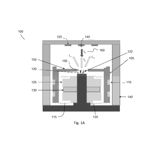
Referring to Fig. 1A, an illustrative schematic of an embodiment of a seismic
system 100
featuring optical readout is shown. The system 100 includes a coil-wrapped
bobbin 105
suspended in the presence of a magnetic field which serves as the proof-mass
structure. The coil
110 facilitates magnetic actuation and is wound around the bobbin such that
there are two
electrical connection terminals to the coil 110. In some embodiments, the
bobbin 105 is
suspended by springs 115 (e.g., a spider spring). For example, the inner ring
of the spring 115
12
CA 02890298 2015-04-07
WO 2014/058472
PCT/US2013/032584
may be rigidly coupled to an inner core 135 while the outer ring of the spring
115 may be rigidly
coupled to the proof-mass structure or bobbin 105. A magnet 130 (e.g., a ring
magnet) and
magnet caps 125 can also be rigidly coupled to the inner core 135 which is
further rigidly
coupled to a housing 140 that serves as the outer casing of system 100. The
housing 140 may be
magnetically permeable and complete a magnetic circuit. The axially polarized
magnetic field
supplied by the magnet 130 is directed by the magnet caps 125 to traverse an
air gap between the
magnet caps 125 and the housing 140 where the coil-bobbin 105 is located. The
resulting
structure 100 enables relative motion between the coil-bobbin 105 and the
housing 140. In
operation, when used as a seismic sensor, both the housing 140 and the inner
core 135 are rigidly
coupled to the ground motion while the proof-mass coil-bobbin 105 is free to
move relative to
the housing 140. As will be understood by those skilled in the art, in various
embodiments other
suitable arrangements may be used to provide a proof mass that is free to move
in a magnetic
field relative to a housing.
To detect and measure the relative displacement of the proof-mass 105 with the
housing 140, the
system 100 may include an opto-electronic detection scheme. The opto-
electronic detection
scheme may include an interferometric scheme in which light 160 from a light
source 145 (e.g., a
laser or light emitting diode, as shown a vertical cavity surface emitting
laser ¨ "VCSEL") is
divided and caused to travel along at least two different paths (e.g., lo, hi
and Li) having an
optical path length difference that depends on the relative displacement of
the proof-mass 105
and housing 140. For example, the light source 145 may emit light Im which may
travel through
a diffraction grating 150 rigidly coupled to the proof-mass 105 via a grating
holder 155. The
light I,õ may then reflect off of a mirror 120 that is rigidly coupled to the
inner core 135 and
travel back through the diffraction grating 150, where the gap height between
the mirror 120 and
the diffraction grating 150 is d 122. The diffraction grating 150 may divide
the light 160 into
light rays lo, hi and Li. A photodetector 125 may detect the resulting
interference pattern that
depends on the optical path length differences (e.g., differences between at
least two of lo, hi and
14). In some embodiments, mirror motion 120 is therefore coupled to ground
motion when the
sensor is used in seismic detection. This configuration may be reversed so
that the motion of the
diffraction grating 150 is coupled to ground motion and the mirror 120 is
coupled to proof-mass
105.
13
CA 02890298 2015-04-07
WO 2014/058472
PCT/US2013/032584
In some embodiments, the arrangement shown can produce an interference pattern
having a
zeroth order peak (Jo) and two first order peaks (hi or ti). In this
illustrative example, three
photodiodes 125 are positioned to detect the intensity of these peaks. The
relative strength of the
intensity of the zeroth order peak (Jo) in comparison to the intensity of the
first order peaks (hi or
Li) may be indicative of the displacement between the proof-mass 105 and
housing 140. In other
embodiments, the arrangements can produce interference patterns having a
plurality of higher
order peaks, and a plurality of photodiodes can be configured to detect the
peaks.
Fig. 1B shows a perspective view of system 100 with additional details. Fig.
1C shows a side
cross sectional view of the system of Fig. 1B. In brief overview, and in some
embodiments,
system 100 includes an optoelectronics printed circuit board (PCB) 165
configured to generate
(e.g., using a laser or light emitting diode), detect and/or control a light
beam. The
optoelectronics PCB may be coupled to the housing 140 such that the PCB may
tilt based on the
orientation of the system 100 with respect to the surface of the ground. The
system 100 may
include a photodiode array ("PDA") 170 configured to act as a position sensor.
The PDA 170
may include a plurality of photodetectors (e.g., photodiodes) capable of
converting light into
either current or voltage. The system 100 may include a focusing lens 175
configured to focus
the light beam 160 emitted from the light source 145 prior to the light beam
160 traveling
through the diffraction grating 150.
Still referring to FIGs. 1B and 1C, in further detail, the proof-mass bobbin
105 may include a
spindle or cylinder on which the coil 110 can be wound. The bobbin 105 may be
made partially,
substantially, or even entirely of a non-conductive or weakly conductive
material such as
aluminum. For example, the bobbin 105 may be made out of a material that may
reduce or
eliminate eddy-current damping.
The coil 110 may be wrapped or wound around bobbin 105 such that there are two
electrical
connection terminals to the coil which may receive an electrical current. The
coil 110 may be
made out of any wire or material capable of being wound around a bobbin and
conducting
electricity.
The system 100 can include springs 115 configured to suspend the bobbin 105.
In some
embodiments, the system 100 includes one or more springs 115 coupled to the
bottom of the
bobbin 105 and a rigid inner core 135, and one or more springs coupled to the
top of the bobbin
14
CA 02890298 2015-04-07
WO 2014/058472
PCT/US2013/032584
105 and the rigid inner core 135. In some embodiments, the springs 115 can
include, e.g., a
spider spring, compression spring, conical compression spring, torsion spring,
barrel spring,
magazine spring, air spring, leaf spring, micro springs, rubber springs,
urethane compression
springs, curved or wave washers, clover dome, and/or wave springs. In some
embodiments, the
spring 115 includes a 3-arm spider spring made from a non-ferrous and/or
nonmagnetic material
such as Beryllium Copper or Inconel.
In some embodiments, the system 100 includes a mirror 120 rigidly coupled to
the inner core
135 that is capable of reflecting the light beam 160 from light source 145.
For example, the
optical element (e.g. grating) and mirror may be placed in close proximity,
e.g., a distance less
than 200, less than 100, or less than 50 optical wavelengths of the light used
to detect
displacement. The mirror 120 may be configured to reflect one or more
wavelengths of the light
beam 160. In some embodiments, the mirror 120 is a plane mirror which has a
flat surface,
while in other embodiments the mirror 120 may include a curved mirror (e.g.,
concave) to focus
the light beam 160. Mirror 120 may have a reflectivity of at least 90%, at
least 95%, at least
99% or more for wavelengths of light in a selected range. In some embodiments,
mirror 120
may include an optical coating in order to alter the way in which the optic
reflects light beam
160. For example, the mirror 120 may include a high-reflector coating which
can be used to
produce mirrors which reflect greater than 99.99% of the received light beam
160 and/or
selectively reflect light over some range of wavelengths.
In some embodiments, system 100 includes a magnet 130 rigidly coupled to the
inner core 135,
which is in turn rigidly coupled to the housing 140. In some embodiments, the
magnet 130 may
not directly be coupled to the inner core; rather, the magnet 130 may be
coupled to the end caps
125 which may be coupled to the inner core 135. The magnet 130 may be
configured to supply
an axially polarized magnetic field to traverse an air gap between the magnet
caps (or "end
caps") 125 and the housing 140. The magnet 130 may be configured to generate
strong electrical
fields in response to motion of the bobbin 105 relative to the housing 140. In
some
embodiments, the magnet 130 includes a permanent magnet, such as, e.g., a rare
earth magnet
(e.g., Neodynium Iron Boron, Samarium Cobalt). In some embodiments, the magnet
130 may
include a ring magnet wherein the inner ring may be rigidly coupled to the
inner core 135. In
other embodiments, the magnet 130 may include a disc magnet, cylindrical
magnet, block
CA 02890298 2015-04-07
WO 2014/058472
PCT/US2013/032584
magnet, cup magnet, or a custom shape magnet configured to provide a magnet
field that enables
the functionality disclosed herein.
In some embodiments, magnet caps or end caps 125 may be placed above and/or
below the
magnet 130. The end caps 125 may be coupled to the inner core 135 and/or
magnet 130. In
some embodiments, the magnet caps 125 is configured to direct a magnet field
supplied by
magnet 130 to traverse an air gap between the end caps 125 and the housing 140
where the
bobbin 105 is located. The end caps 125 may configured in various shapes such
that the end cap
125 may be placed above and/or below the magnet 130. For example, if the
magnet 130 is a ring
magnet, the end cap 125 may be in the shape of a ring similar to that of the
magnet 130.
However, in various other configurations, the end caps 125 may be configured
to provide the
functionality disclosed herein without mirroring the shape of magnet 130.
In some embodiments, the system 100 may include an inner core 135. The inner
core 135 can be
rigidly coupled to the housing 140, magnet 130 and/or end caps 125. In some
embodiments, the
inner core may be made out of a low magnetic permittivity material such as,
e.g., aluminum.
The inner core 135 may be configured in various shapes to provide the
functionality disclosed
herein. For example, the inner core 135 may include an elongated cylindrical
portion and a
flange coupled to the housing 140.
In some embodiments, the system 100 includes a housing 140 that may function
as an outer
casing for the sensor. The housing 140 may be made out of magnetically
permeable material
that is configured to complete a magnet circuit. For example, the housing 140
may have a
magnetic permeability, e.g., about unity (e.g., using aluminum) that may be
sufficient to support
a magnet field provided by magnet 130. In other embodiments, the housing may
be made of
non-magnetic non-ferrous materials and be configured to provide structural
support and/or
couple one or more elements of the system 100 to an external environment. For
example, the
housing 140 may couple a component of the system 100 to external ground
motion, wave
motion, vibrations, impulses, forces, or any other movements or motion that
have an acceleration
and/or velocity component.
In some embodiments, the system 100 includes a light source 145 configured to
supply a light
beam 160 with a wavelength within a range of wavelengths (e.g., 850nm +/- 1
nm). For
example, in some embodiments, the light source 145 may include a laser or
light emitting diode.
16
CA 02890298 2015-04-07
WO 2014/058472
PCT/US2013/032584
In some embodiments, the light source may be a solid state laser, such a
vertical cavity surface
emitting laser. In various embodiments any other suitable laser source may be
used.
The system 100 may include a diffraction grating 150 configured to affect a
light beam 160
supplied by light source 145.
-- In some embodiments, the system 100 includes a grating holder 155 coupled
to the bobbin 105
and configured to hold a diffraction grating 155. The grating holder 155 may
move relative to
the mirror 120.
In some embodiments, the system 100 includes one or more focusing lenses 175
configured to
focus the light beam 160.
-- In some embodiments, the system 100 includes an optoelectronic PCB 165. In
some
embodiments, the optoelectronic PCB 165 may be rigidly coupled to the housing
140. In other
embodiments, the optoelectronics PCB 165 may be coupled to the housing 140 in
a manner that
allows for the optoelectronic PCB 165 to tilt or otherwise move relative to
the housing 140.
In some embodiments, the system 100 includes a photodiode array 170 coupled to
the
-- optoelectronics PCB 165. The photodiode array 170 may be configured to
receive one or more
light beams 160 reflected from the mirror 120 and further configured to detect
an aspect of the
received light. For example, the photodiode array 170 may include a plurality
of photodetectors
configured to detect an intensity of the receive light and also determine a
position of the received
light. The detected light data may be result in an electric signal (e.g.,
voltage/current) that can be
-- used to generate an interference pattern. In some embodiments, the
photodiode array 170 may
include a single dimension of a plurality of photodetectors or photodiodes. In
some
embodiments, the photodiode may include a semiconductor diode with a PIN
junction or p-n
junction.
Referring to Fig. 2, an illustrative functional block diagram of some
embodiments of the sensors
-- of Figs. 1A-1B, with emphasis on the readout electronics 200 is shown. The
readout electronics
200 may be communicatively and/or electronically coupled to the sensor
components 202, which
include the coil 110, light source 145, and photodiode array 170. In some
embodiments, the
signals from the photodiode array 170 are output to readout electronics 200,
where the signals
are processed to generate a signal indicative of the relative displacement of
the proof mass 105
17
CA 02890298 2015-04-07
WO 2014/058472
PCT/US2013/032584
and housing 140 (as shown, an acceleration signal is produced). The two-
terminal coil
connection 110 (or other suitable electrical connection) can be electrically
connected to the
readout electronics 200, which can be configured to apply, based on the
measured displacement
signal, feedback forces to the proof-mass 105 that can adjust the operating
point of the sensor.
In some embodiments, the readout electronics includes force feedback circuitry
205 configured
to apply feedback forces to the proof-mass 105 based on the measured
displacement signal.
In some embodiments, the readout electronics 200 includes one or more
precision voltage
references 210. The precision voltage reference 210 may internal or external
to the readout
electronics 200 and/or system 100. The precision voltage reference 210 may be
configured to
provide a precise voltage reference that may be used by one or more component
of the system
100 and/or readout electronics 200. For example, an MCU 220 may utilize a
precise voltage to
facilitate converting an analog signal to a digital signal (e.g., ADC
functionality). In another
example, the precision voltage reference 210 may be coupled to the light
source 145 via a
resistor and provide the light source 145 with power. The precision voltage
reference 210 may
include one or more components such as, e.g., resistors, inductors,
capacitors, op-amps,
transistors, semiconductors, etc. configured to provide a precise voltage.
In some embodiments, the readout electronics 200 includes one or more
transimpedance
amplifiers 215 coupled to one or more photodetectors and/or the photodiode
array 170. In some
embodiments, the transimpedance amplifiers 215 may be configured to convert
current received
from the photodiode array 170 to voltage.
In some embodiments, the readout electronics 200 includes a microcontroller
unit ("MCU") 220
configured to receive input from one or more component of the readout
electronics 200
including, e.g., the transimpendance amplifiers 215, and force feedback
circuitry 205 and
provide output to same. The MCU 220 may include a plurality of pins to receive
and/or output
analog and/or digital signals. Analog output pins may include, e.g., a pin for
each of a positive
and negative acceleration in the X, Y, and Z directions.
In some embodiments, the MCU 220 includes an analog-to-digital converter
("ADC")
configured to receive an analog signal (e.g., the continuous optical output
voltage/current from a
photodiode array 170 and/or transimpedence amplifier 215) and convert the
analog signal to a
digital number that is proportional to and/or represents the amplitude of the
analog signal. In
18
CA 02890298 2015-04-07
WO 2014/058472
PCT/US2013/032584
some embodiments, the MCU 220 includes a linear ADC; therefore, the range of
input values
may have a linear relationship with the output value. The MCU 220 may be
configured to
sample the analog signal at one or more sample rates including, e.g., 250Hz,
500Hz, lkHz. The
analog signal may be sampled at 24bit, 26bit or 32bit resolution. The sensor
may acceleration to
voltage with a sensitivity of 5V/g using a supply voltage which may vary from
6V to 17V. The
passband of the sensor may be from .01Hz to 3kHz.
In some embodiments, the MCU 220 may include a proportional-integral-
derivative controller
("PID controller") and/or a proportional-derivative controller ("PD
controller") or otherwise be
configured to provide feedback controller functionality. For example, the MCU
220 may
calculate an "error" value as the difference between an output voltage
indicative of a measured
process variable (e.g., measured displacement of the proof-mass 105 relative
to the housing 140)
and a desired setpoint (e.g., corresponding to a fringe "lock" and/or
mechanical zero). The MCU
220 may attempt to minimize the error by adjusting the process control inputs
(e.g., effective
spring force applied by coil 110).
In some embodiments, the MCU 220 may be configured to control where on the
output voltage
curve 305 of Fig. 3A the system 100 is operating.
Referring to Fig. 3A, an illustrative plot of the output voltage 305 of the
photodiode array 170 as
a function of the relative displacement of the proof-mass 105 and housing 140
is shown. For
example, the output voltage 305 may correspond to the relative intensity of
the zeroth (I0) and
first order diffraction peaks (Li and Li). The output voltage 305 may be
periodic (as shown
sinusoidal), with a period that is proportional to the inverse of the
wavelength of the light 160
used to generate the interference pattern. As used herein, the term fringe 315
may refer to one
half period of the output voltage signal.
In various embodiments, during operation, it may be desirable for the system
to operate within a
range of displacements corresponding to a single fringe 315. In some
embodiments, it may be
desirable for the system to operate within a range of displacements
corresponding to a portion of
a single fringe where the output voltage varies substantially or at least
approximately linearly as
a function of displacement (as shown by reference 325 of Fig. 3B).
In some embodiments, it may further be desirable for the system to operate
within a range of
displacements corresponding to a single fringe 315 at mechanical zero 320. For
example, a
19
CA 02890298 2015-04-07
WO 2014/058472
PCT/US2013/032584
fringe at mechanical zero 320 may result in an optical output voltage of or
near zero volts, which
may reduce power consumption. As the system 100 operates on fringes farther
from mechanical
zero, the mechanical spring force increases and therefore DC offset also
increases. This increase
in DC offset may also cause adverse dynamic range issues in a Analog-to-
Digital converter
(ADC).
As shown in the plot, the displacement is indexed to the "mechanical zero" 320
of the system
100. When no feedback current is applied to the coil 110, the spring mass
system may vibrate
due to, e.g., ground motion. In this state, the system 100 may have a
relatively high quality
("Q") factor (e.g., an underdamped system with a low damping ratio) and may
primarily oscillate
at a natural frequency. The average location of the proof-mass 105 is
determined by tilt angle,
i.e., force of gravity pulling on the spring-mass system along the direction
of motion of the
system 100. This can be considered the natural resting point of the spring 115
and may be
referred to as "mechanical zero" 320. By turning on the feedback control
system, as discussed
further herein, the Q factor may be lowered, resulting in an overdamped system
with a high
damping ratio. This may result in a system 100 that may be less susceptible to
oscillations due to
the impact of noise; e.g., the system may not oscillate or have a minimum
oscillation frequency
when in equilibrium, and when displaced by (e.g., by ground motion) may return
to the
equilibrium state via exponential decay. In some embodiments, the system may
have a Q factor
between the range of 0.1 to 5 (wherein Q factor = 1/(2*damping factor)).
The output voltage response curve 305 shown in Fig. 3A may be an idealized
version of a
response curve. In some embodiments, the output voltage response curve 305 may
be modified,
e.g., by an envelope function that depends on the gap distance between the
mirror 120 and
diffraction grating 150. Accordingly, the fringes 315 may have differing
optical modulations.
Optical modulation for a given fringe as used herein refers to the peak-to-
peak swing of the
optical curve normalized to a peak value of the optical curve, typically
corresponding to
mechanical zero (100% is perfect modulation, above 30% may be advantageous for
typical
sensor operation). In various embodiments, using the techniques described
herein, the system
can be locked to a fringe 315 having an optical modulation of at least 30%,
40%, 50%, 60%,
70%, 80%, 90%, 95% or more, e.g., in the range of 30%-100% or any subrange
thereof.
CA 02890298 2015-04-07
WO 2014/058472
PCT/US2013/032584
In some embodiments a given fringe 315 may have a nonlinearity or other
undesirable feature or
artifact, e.g., caused by a defect in the optical system.
The amount of proof-mass 105 displacement depends on ground motion, but, in
some
embodiments, even a quiet environment will likely move the equivalent distance
of multiple
-- optical fringes 315 in the absence of force feedback. Accordingly, the
feedback coil 110 is used
to maintain or "lock" the sensor to a desired operating point and displacement
range.
Referring to Fig. 3B, in some embodiments, when the sensor is powered a
control system MCU
220 (shown in Fig. 2) may be configured to lock the system 100 on one optical
fringe 325. The
MCU 220 can provide the functionality of a proportional-differential "PD"
controller, a
-- proportional-integral-differential" PID" controller, or other suitable
controller. In some
embodiments, the controller can be designed to operate on one or more slopes
and function in a
manner similar to a damped mass-spring system with a natural frequency that is
substantially
larger than the natural frequency of the open loop system. Note that, in
various embodiments, the
system can operate on either positive or negative slopes of one fringe 315 in
the optical curve,
-- depending on the selected polarity of the feedback loop. Exemplary feedback
loop
implementations are shown in Figs. 6-8.
In some embodiments, the initial fringe locked on is determined by the
position of the proof-
mass 105 when the sensor was powered on. Naturally, it is normally located
near mechanical
zero, but exact location can vary.
-- As shown in Fig. 4, the amount of mechanical force applied by the spring
115 depends, at least
in part, on the proof-mass 105 position relative to mechanical zero 320, and
the amount of force
applied by the feedback coil 110 can be determined by the output of the
optical system. For
example, to operate at or near mechanical zero, the system can apply an offset
power (e.g., DC
offset or current offset) such that the proof-mass 105 operates at or near
mechanical zero or
-- within a fringe. When the system 100 is operating on a non-ideal fringe
(i.e., located at one or
more fringes away from mechanical zero 320) sensor performance may be
negatively affected.
For example, increased offset voltage can mean reduced dynamic range,
increased power
consumption, and reduced random intensity noise cancellation.
Accordingly, in some cases, the system is configured to operate at a fringe
located closest to
-- mechanical zero 320 to minimize the mechanical spring force and offset
voltage. However, in
21
CA 02890298 2015-04-07
WO 2014/058472
PCT/US2013/032584
some cases it may be desirable to operate on a fringe away from mechanical
zero. For example,
the output response at the fringe closest to mechanical zero may be distorted
due to some
imperfection in the system optics, while another fringe is relatively free
from imperfection. In
such cases, it may be desirable to operate on the latter fringe.
The operating fringe can be monitored by reading the offset voltage and can be
changed with a
variety of methods in response to various conditions as described herein. For
example, the
system 100 may experience mechanical drift due to acceleration caused by,
e.g., spring settling,
temperature expansion, etc. Referring to Fig. 3A, drift can cause the voltage
output curve 305 to
translate laterally in either direction. When force feedback is applied, the
system 100 can lock
onto one fringe. However, in the event mechanical drift occurs, this fringe
may drift
substantially away from the ideal fringe, causing a corresponding drift in the
feedback coil 110
offset voltage. The techniques described herein may correct for drift by
shifting the operating
point from the drifted fringe back to a fringe closer to mechanical zero.
In some embodiments, if the sensor receives a large enough signal to overwhelm
the control
system (e.g., a temporary mechanical shock) the proof mass 105 may move beyond
the fringe it
is operating on. This may result in the control system no longer operating as
an overdamped
mechanical oscillator. Instead, the sensor may exhibit open-loop
characteristics (for instance
oscillating at the open loop natural frequency). As the input acceleration
settles, the system can
re-lock on to a fringe. This fringe may or may not be ideal, and may have
substantial offset
voltage. The techniques described herein my be used to correct for drift by
shifting the operating
point from the drifted fringe back to a fringe closer to mechanical zero.
Fig. 5A is an illustrative graph of the optical signal non-idealities (e.g.,
non-linerity and decaying
envelope) in accordance with an embodiment. In this illustration, the graph
plots the optical
signal level (volts) versus the mirror to grating gap height (microns), for
the optical signal level
505 and the total optical power 510. Referring back to an embodiment
illustrated in Fig. 1A, the
mirror to grating gap height may be the distance 122 between mirror 120 and
diffraction grating
150.
In this example, when the mirror to grating gap height 122 is between 0 and
approximately 70
microns, the system may exhibit non-linear optical behavior where the optical
signal level 505
has an envelop as high as -0.8 to 0.8 volts or more, and oscillates between
this envelope.
22
CA 02890298 2015-04-07
WO 2014/058472
PCT/US2013/032584
Accordingly, the corresponding total optical power graph 510 shows the optical
power varying in
this non-linear region. This region of non-linear optical linear behavior 515
may be the result of
one or more factors, including, e.g., internal reflections. Within the region
515, as the gap height
122 increases from 0 to 70 microns, the envelope may decay from -0.8 to 0.8
volts to
approximately -0.6 to 0.6 volts.
Thereafter, as the gap height 122 increases beyond approximately 70 microns,
the system may
achieve static equilibrium where the proof mass falls within a satisfactory
window of operation
520. In this example, the system can operate in static equilibrium when the
gap height 122 is
between approximately 85 microns and approximately 150 microns. Furthermore,
the total
optical power 510 in the window of operation 520 remains steady at, e.g.,
approximately
200microWatts. The optical signal continues to decays as the gap height
increases beyond 150
microns, as shown ion region 525.
Fig. 5B shows a zoomed-in view of the optical curves that highlights the
optical signal as it
transitions from the non-linear region 515 to the window of operation region
520. Region 540
represents a region between the non-linear region 540 and the window of
operation region 520
where the envelope has decayed substantially, but not yet reached a static
equilibrium.
Fringe Selection Techniques
As noted above, as the system 100 operates in fringes that are farther from
mechanical zero, the
mechanical spring force increases, which can increase the DC offset. In some
embodiments, an
increased DC offset may increase power usage and adversely impact the dynamic
range when the
analog optical read out signal is converted to a digital signal, e.g., using
an analog to digital
converter (ADC). Furthermore, depending on the performance of the optical
system, some
fringes may not be sufficiently linear and/or may not have sufficient optical
modulation.
Referring to Fig. 6, an electronic circuit used to provide coil polarity
toggling to allow fringe
selection is shown. The circuit can include two positive coil drives 605 and
615 coupled to
opposing ends of the coil 110 via a switch or toggle 620 and 625, and a
negative coil drive 610
coupled to both the positive coil drives 605 and 615 via the switches 620 and
625. When the
polarity of the feedback coil 110 is reversed via switches 620 and 625, the
operating point of the
system 100 moves to the closest opposite polarity slope of the output voltage
response curve.
23
CA 02890298 2015-04-07
WO 2014/058472
PCT/US2013/032584
Because the mechanical spring 115 applies force in the direction of mechanical
zero, the system
may move one fringe in that direction. The system is stable at either
polarity.
This process can be repeated, hopping one fringe per repetition, until the
system 100 arrives at a
desired fringe, e.g., the fringe at or near mechanical zero. Operating on this
fringe may result in a
lower DC offset and reduce power consumption while maximizing dynamic range.
In various embodiments, toggling can be accomplished by using an analog switch
(e.g., a
MOSFET transistor), relay, or any other electronic switching technique 620.
This switching
technique 620 can be initiated by a microcontroller, analog circuit, digital
circuit, or any other
type of logic include in the readout electronics 200.
Note that typically, polarity toggling will only move the mass towards
mechanical zero. This is
advantageous for reducing offset, but may not provide a solution to problems
with fringe
linearity or modulation.
In some embodiments, the selected fringe can be adjusted either towards
mechanical zero or
away from mechanical zero via an injection current applied to the coil 110.
For example, to
reduce offset, the mass can be can be pushed to a fringe that is closer to
mechanical zero. In
another example, if a fringe that the sensor is operating on has poor
linearity or modulation, the
surge current can be used to push the mass to a nearby fringe that has better
properties. The
surge current can adjust the fringe by sending a sufficiently large surge of
current through the
coil that temporarily overwhelms the feedback system. The injection current
pulse can be
calibrated to push the mass a number of fringes in either direction. In some
embodiments, the
system 100 can reduce the loop gain to facilitate adjusting the operating
fringe. In some
embodiments, the operating fringe can be adjusted by mechanically moving the
proof mass, e.g.,
using a mechanical servo.
In some embodiments, fringe selection may be accomplished using open loop
toggling. By
opening the feedback loop, the system may respond to ground motion according
to its open loop
transfer function. Upon reapplying feedback control, the system can then
fringe lock on the
nearest operating point, which may be close to mechanical zero. Open loop
toggling can be
implemented in a number of ways, including, e.g.,: temporarily disconnecting
the feedback loop
(using a switch, relay, etc.), temporarily disabling the optical displacement
sensing (e.g., by
disabling the laser or photodetectors), or temporarily removing or reducing
power from system.
24
CA 02890298 2015-04-07
WO 2014/058472
PCT/US2013/032584
In general, open loop toggling is advantageous in that it may be easy to
implement, but offers
limited ability to control the resulting operating fringe.
Fringe Counting
In order for the system to determine when to change fringes, capability for
analyzing the status
of the current fringe may be provided, e.g. using the techniques described
below.
For applications where only voltage offset reduction is desired, the system
can monitor fringe
location by reading DC offset using any suitable technique, e.g., using a
microcontroller,
comparator, volt meter, etc.
In some embodiments, the system 100 includes a secondary detector configured
to measure the
displacement between the housing and proof mass (e.g., by measuring the gap
between the
mirror and grating as shown in Fig. 1). The secondary detector can be
configured to resolve the
displacement at distances corresponding to the wavelength of the laser. This
technique is
particularly useful if an integrator is used in the feedback loop used to lock
to a fringe. An
integrator can remove the DC offset voltage from the output (obviating the
need for DC offset
monitoring), but would not solve all of the inherent issues involved with
electromagnetically
holding the mass away from its natural resting point such as increased power
consumption. In
such cases the secondary detector can be used to determine if the system is
operating at a fringe
away from mechanical zero, and cause adjustments to be made accordingly.
In some embodiments, the system 100 can evaluate fringe quality, e.g.,
identifying nonlinearity
or poor modulation in a fringe. For example, the modulation efficiency or
linearity of a fringe
can be determined by conducting a sweep of the optical response curve. The
optical sweep can
be performed by opening the feedback loop and actuating the proof mass through
several fringes
while measuring the generated output voltage signal from the optical readout
system. The
resulting waveform may be analyzed using any suitable technique including,
e.g., by using an
ADC, comparator scheme, Schmitt trigger, etc. From this result, the modulation
efficiency and
linearity of a fringe can be determined. In some embodiments, the optical
sweep is performed
periodically during the deployment of the sensor using internal components of
the sensor. In one
embodiment, the optical sweep is performed prior to deployment, e.g., using an
external testing
set up, and the results stored on board the sensor for use.
CA 02890298 2015-04-07
WO 2014/058472
PCT/US2013/032584
Photocurrent Subtraction
As described with reference to Figs. 1 and 2, in some embodiments, the proof
mass position
signal is determined based on the difference between the inside (zeroth) and
outside (first)
optical orders of the optical interference pattern. In some embodiments, the
readout electronics
200 can be configured to determine this difference. This difference signal
represents the
system's output as well as the feedback loop error signal. In some
embodiments, the laser's
random intensity noise (RN) will be captured in each order. Subtracting these
signals works to
cancel out RN.
Figs. 7-9 show circuit implementations for various subtraction schemes. In
brief overview, Figs.
7-8 show implementations of techniques where each photocurrent can be
amplified and
conditioned independently. For example, Fig. 7 illustrates an implementation
of a differential
coil drive technique where the two optical orders 705 and 710 can be placed on
opposite
terminals of the feedback coil 110 and the system output (acceleration,
velocity, etc.) can be
presented as a balanced signal pair and be fed into a differential amplifier.
In another example,
Fig. 8 illustrates an implementation of an active photocurrent subtraction
technique where the
two resulting voltages can then be subtracted in an analog or digital circuit,
which can either be
ground-referenced or differential, and can supply amplification. In yet
another example, Fig. 9
illustrates an implementation of passive photocurrent subtraction where the
photocurrents from
each optical order can be placed in parallel with opposite polarities.
Referring to Fig. 7, and in further detail, the circuit may include a
plurality of photodiodes 705
corresponding to the first optical order and a photodiode 710 corresponding to
the zeroth optical
order. For example, the first optical order may include two peaks that may be
detected by the
two photodiode while the zeroth optical order may include one peak detected by
a single
photodiode. The photodiodes 705 of the first optical order may be coupled to
the V_ or inverting
terminal of an operational-amplifier ("op-amp") 720. Negative feedback may be
provided by
resistors and 715 (e.g., a resistor, or an analog or digital variable
resister/potentiometer that can
adjust a trans-impedance gain) coupled to the non-inverting input terminal and
Vout. Similarly,
the output of the photodiode corresponding to the zeroth optical order 710 may
be coupled to the
non-inverting input of a op-amp 725. Op-amp 725 may include a negative
feedback resistor 730
(e.g., a resistor, or an analog or digital variable resister/potentiometer
that can adjust a trans-
26
CA 02890298 2015-04-07
WO 2014/058472
PCT/US2013/032584
impedance gain) coupled to the non-inverting input terminal and Vout. The
output of the op-
amps is directed to the feedback network 740 and 735 used for closed loop
control of the signal
provided to the coil 110.
Figure 8 shows an active photocurrent subtraction technique. The photocurrents
representing
optical order 1 705 and optical order 0 710 are amplified and conditioned
independently. For
example, the optical order 1 705 photocurrent can be amplified and conditioned
via amplifier
720, and the optical order 0 photocurrent 710 can be amplified and conditioned
via amplifier
725. The two resulting voltages are then subtracted in an analog or digital
circuit. This circuit
can be either ground-referenced or differential, and may also apply
amplification. For example,
the difference between the resulting voltages can be obtained via differential
amplifier 810. The
output of the op-amp 810 is directed to the feedback network 815 used for
closed loop control of
the signal provided to the coil 110.
Figure 9 shows a passive photocurrent subtraction technique. The photocurrents
from each
optical order can be placed in parallel with opposite polarities. For example,
the photocurrent
representing optical order 1 705 is in parallel with the photocurrent
representing optical order 0
710. The difference between the photocurrents 705 and 710 can take place in
the current domain
and this resulting difference current can then be amplified in a single
amplifier (e.g. a trans-
impedance amplifier ¨ "TIA") 720 and 715, presenting an output and a feedback
voltage. The
output of the amplifyer 720 is directed to the feedback network 905 used for
closed loop control
of the signal provided to the coil 110.
Modulation Correction
As noted above, in some embodiments, all fringes do not have the same
detection sensitivity.
Fringe detection sensitivity (e.g., amps /m/s/s) may vary based on the
mirror/grating gap (tilt
angle), manufacturing tolerances, and/or other factors. Detection sensitivity
decreases as the gap
between the mirror and grating increase. Thus, there may be a decline in
detection sensitivity
when the sensor is positioned in an orientation such that gravity pulls the
grating and mirror
apart. Changes in detection sensitivity affect the dynamic range of the closed-
loop system.
In some embodiments, the amount of photocurrent received by each order in the
interference
pattern may not be equal. This can vary by design, manufacturing tolerances,
tilt angle, and other
issues. If photocurrent signals are not balanced, system dynamic range is
compromised because
27
CA 02890298 2015-04-07
WO 2014/058472
PCT/US2013/032584
the more sensitive order will be more prone to clipping the amplifier.
Secondly, RN
cancellation (as described above with reference to photocurrent subtraction)
may be improved or
maximized when each order is equal
Several techniques may be used to mitigate or eliminate these issues,
including, e.g., variable
TIA gain, Post-TIA gain, a shunt resistor, post-TIA voltage divider, or a
current mirrpor/active
photocurrent balance scheme. For example, in the variable TIA gain stage,
variable gain
amplification can be provided by a variable resistor or potentiometer placed
in the TIA feedback
loop. In some embodiments, other programmable gain amplifier schemes, a
suitable logic
element or other control electronics can set TIA gain accordingly. Figs. 7 and
8 illustrate
techniques where separate variable gain TIAs (e.g., 715 and 730) are provided
for the zeroth
order photodiodes and the pair of first order photodiodes. Fig. 9 shows a
scheme where a single
variable gain TIA 715 is provided after the zeroth and first order
photocurrents have been
subtracted in the current domain.
Fig. 10 shows a shunt resistor technique to adjust TIA gain in accordance with
an embodiment.
In this illustration, a resistor 1015 and 1010 (e.g., a variable resistor or a
potentiometer) can be
placed in parallel with one or both photodiodes to siphon off photocurrent as
necessary to
balance the two orders.
Other techniques may include a post-TIA gain stage where an additional
variable gain stage can
be placed after the TIA using similar methods; a post-TIA voltage divider
where a variable
voltage divider can be placed after the TIA stage (but before subtraction) to
adjust the
photovoltages until the zeroth and first order signals are balanced; and a
current mirror / active
photocurrent balance scheme or any other suitable active circuit designed to
be used to balance
photo currents.
Non-modulated Photocurrent Removal
As will be apparent to one skilled in the art, in some embodiments, the
detection photodiode
output will include a non-modulated photocurrent component that is not a
function of grating and
mirror position. This component may be caused, e.g., by stray light within the
sensor housing
(e.g., from secondary reflections in the optical system). This non-modulated
photocurrent is not
useful as signal, but nonetheless gets amplified by the TIA, and can cause the
amplifier to clip.
28
CA 02890298 2015-04-07
WO 2014/058472
PCT/US2013/032584
In various embodiments, the following techniques may be used to reduce or
eliminate the non-
modulated photocurrent.
In some embodiments, passive photocurrent subtraction may be used to reduce or
eliminate
constant photocurrent in the current domain, preventing problems with
amplifier circuit.
Fig. 11 illustrates an opposing current injection technique that can be used
to reduce or eliminate
the non-modulated photocurrent in accordance with an embodiment. As shown, a
current source
1105 and 1110 (using any suitable topology, possibly variable) can be placed
in parallel with
each photocurrent signal 705 and 710 to remove the non-modulated or constant
component. The
resulting individually conditioned photocurrent can be individually amplified
via amplifiers 1115
and 1125.
In some embodiments, in addition or alternative to the above techniques, the
amplifier voltage
can be increased such that the amplifier can no longer clip, providing a
"brute force" solution to
the clipping issue.
Switchable Eddy Current Damping "Handbrake"
Fig. 12 illustrates a technique for changing the damping of the open-loop
system in accordance
with an embodiment. As noted above, in some cases it is desirable to turn off
closed loop
feedback and allow the system to operate open loop, and/or change the damping
of the open-loop
system in real-time. As shown in Fig. 12, and in some embodiments, variable
open-loop
damping can be provided by shunting the coil 110 to a damping resistance 1205.
This damping
resistance 1205 may be variable, and it can be placed in series with a
switching element 1210
such as an analog switch or relay. The switching element 1210 can be
modulated, e.g., with a
selected duty cycle or a selected frequency. The shunt, when switched into the
circuit, provides
increased damping, thereby operating as a so-called "handbrake" to the
mechanical system.
This handbrake may be used in several applications including the following.
The handbrake may
be activated when using coil polarity toggling (e.g., for fringe selection) to
prevent unwanted
oscillations. The handbrake may be activated when system is receiving large
signals (e.g., a
temporary mechanical shock) to aid clip recovery. The handbrake may be
activated when system
is powered off to reduce damage from vibrations during shipping. The handbrake
may be
activated if the system becomes unstable or oscillates.
29
CA 02890298 2015-04-07
WO 2014/058472
PCT/US2013/032584
Real-time Adjustment of Loop Gain
In some applications, it may be desirable to precisely adjust the amount of
loop gain in the
system in real-time. In some embodiments, the feedback network that determines
loop gain can
contain variable components. In addition, analog switches or relays can be
placed in the feedback
loop and toggled with a duty cycle and frequency.
Applications include reducing loop gain when attempting to reposition proof
mass as described
in the section titled Fringe Selection above. This reduces the amount of force
required to
overwhelm the feedback system. Also, when transitioning from open-loop to
closed-loop (for
instance after power on), loop gain can be steadily increases rather than
suddenly turned on to its
full value.
In some embodiments, it may be advantageous to measure and control the nominal
gap spacing
between grating and mirror in an effort to adjust the set point or operating
point of the sensor.
For example, in some embodiments, there is a natural sag of the proof mass due
to its own
weight. The level of sag depends on the orientation and inclination of the
sensor. It may be
advantageous for the sensor to achieve the same operating point regardless of
inclination, and
this "tilt compensation" can be achieved through one or more the following
techniques. As a
way to sense sag, a secondary sensor (e.g. an inclinometer) may be used to
sense inclination
which is correlated with sag. As a way to sense sag, use wavelength of optical
readout light as a
length measurement through periodicity properties of the optical curve to set
optimal gap. As a
way to control the nominal gap spacing between grating and mirror, actuate
diffractive optical
element using any of suitable actuators (i.e. piezoelectric, magnet coil,
electrostatic, motor drive,
pneumatic) to achieve nominal gap distance. As a way to control the nominal
gap spacing
between grating and mirror, actuate mirror using any suitable actuator (i.e.
piezoelectric, magnet
coil, electrostatic, motor drive, pneumatic) to achieve nominal gap distance.
As a way to control
sag, coil on bobbin may be driven with a current to levitate bobbin at desired
position.
Various embodiments described herein use of optical elements (e.g., a mirror
and a grating)
mounted to the proof mass and the housing to provide optical readout of the
relative
displacement between the proof mass and the housing. These optical elements
may include
various features or techniques to provide the optical readout. For example,
the optical element
can include a ruled grating on an optically transparent substrate for
splitting light into two beams
CA 02890298 2015-04-07
WO 2014/058472
PCT/US2013/032584
(a reflected beam and a transmitted beam). The substrate can be made
transparent using anti-
reflective coating. In some embodiments, the ruled grating can include two
layers, where a 1st
layer reflects at a 1st rate and a 211" layer reflects at a 211" rate. In some
embodiments, the rulings
of the ruled grating can be of a fixed pitch. For example, the pitch of the
rulings can be based on
the width of the ruling line ("x") and the gap width between ruling lines
("y"), where the pitch is
equal to x+y.
In some embodiments, the top of the ruled grating may include a thin
protective layer which
prevents ruling lines from making contact with reflecting mirror surface. In
this or other
embodiments, the protective layer may be fabricated on the surface of the
mirror.
Optical Sensor
Referring to Fig. 13, an illustration of a system that actively guides light
from the optoelectronics
board 165 to the grating 150 in a closed loop scheme in accordance with an
embodiment is
shown. For example, one or more of the lens, light source, and optoelectronic
board may be
mounted on a servo (e.g., magnetic or piezoelectrically actuated) to guide the
light ray 160. To
sense the success of the alignment, a current may be fed to the bobbin coil
110 to actuate or
vibrate the bobbin 105 while reflected beams are monitored.
In some embodiments, it may also be advantageous to control the planarity
between mirror 120
and grating 150 surfaces. Mirror 120 and/or grating 150 inclination may be
actuated using
magnetic or piezoelectric actuation to control planarity. Properties of the
reflected beams may
be measured and monitored at the optoelectronic board to determine when
planarity is adjusted
to a desired location. The coil may be fed current to create a signal for use
in this adjustment.
In some embodiments, the system may include optical positioning mount 1305 and
beam
steering mirrors 1310 to guide the light beam 160.
Figs. 14A-B illustrate concepts of using a diffraction grating to split beams
in a
microinterferometer. This concept has been utilized in measuring precise
relative displacements
and is disclosed in U.S. Pat. No. 7,518,737 entitled "Displacement-measuring
optical device with
orifice". The diagram of Fig. 14A and Fig. 14B illustrate two scenarios. In
Fig. 14A, a first
scenario 1401 shows what occurs when a target surface 1404 is placed a
distance of a half-
wavelength, k/2, away from a reference point, in this case, a reflective
diffraction grating 1405.
31
CA 02890298 2015-04-07
WO 2014/058472
PCT/US2013/032584
In Fig. 14B, a second scenario 1402 shows what occurs when the target surface
1404 is placed a
distance of a quarter-wavelength, k /4, away from the diffraction grating
1405. The detailed
diffraction pattern of such a structure can be found by applying standard
diffraction theory to
determine the locations and the dimensions of the photo-detectors or light
guide apertures.
In both instances, the reflective diffraction grating 1405 is formed on a
transparent substrate
1403. Non-limiting examples of materials that can be used to construct the
substrate are quartz,
silicon, sapphire, glass, and combinations thereof The diffraction grating
1405 can be formed of
an array of diffraction grating fingers 1406 equally spaced along a front edge
of the transparent
substrate 1403. The diffraction grating fingers 1406 could have a height on
the order of micro- or
nano-meters.
In the first scenario 1401, when an incident light is illuminated through the
transparent substrate
1403, a first portion of the incident light is reflected from the reflective
diffraction grating 1405.
A second portion of the incident light is transmitted and diffracted about the
diffraction grating
fingers 1406. The transmitted and diffracted light reflects off of the target
surface 1404 and is
measured by a proper detection unit (not shown), such as a photo-detector or a
photo-diode. As
in scenario 1401, the target surface is placed at a distance of k /2 or any
integer multiple, thereof
In this case, the zeroth order of the transmitted incident light is reflected
back. In general, the
zeroth order is the transmitted light that is illuminated directly, in which
case no diffraction, or
change in direction occurs. The first portion of the incident light, and the
second portion of the
incident light which has been reflected off of the target surface 1404
interferes with each other.
The phase of the two portions of the light waves help form constructive and
destructive
interference patterns. From the interference patterns, the relative distance
between the diffraction
grating 1405 and the target surface 1404 can be determined.
In scenario 1402, the same general structure is set up. In this case, the
target surface 1404 is
placed a distance of k/4 away from the diffraction grating 1405. In practice,
the target surface 4
may be placed at any integer multiple of k/4 and the same general results will
occur. When the
first portion of the incident light joins with the second portion of the
incident light upon
reflection, destructive interference cancels out the two. The second portion
of the light travels an
extra distance of 2 times the distance between the target surface 1404 and the
diffraction grating
1403, which results in a phase difference between the two portions of it,
complete destructive
32
CA 02890298 2015-04-07
WO 2014/058472
PCT/US2013/032584
interference. On the contrary though, the higher order diffraction fields,
such as the first order,
can constructively interfere with the first portion of the incident light. As
Figs. 14A and 14B
depict, the higher order first and second portions of the incident light are
angled and not parallel
to the line of illumination, like the zeroth order beam.
Fig. 15, illustrates a variation of the optical system illustrated in Fig. 13,
where the total beam
path length between the source and the diffractive optic element is increased
using one or more
optical elements (as shown two mirrors). As shown in the lower inset, the
overall effect is
equivalent to positioning the source at a virtual position at a greater
distance from the grating and
mirror. In some embodiments, this may advantageously provide improved depth of
focus at the
grating/mirror.
Figs. 16-17 illustrate a specially designed grating that may be used to
provide enhanced
performance at a targeted wavelength. The grating includes a substantially
transparent substrate
(e.g., a glass substrate) on which a lined diffraction grating has been
formed. The lined grating is
formed as a thin film, e.g., with a total thickness of less than about 50 nm.
The grating is formed
with a bilayer structure. The top layer is chosen to have relatively low
reflectivity (e.g., less than
3%), while the bottom layer has relatively high reflectivity (e.g., about 50%
or greater). As
shown in Fig. 17, this structure operated to reduce multiple reflections
between the grating and
mirror, thereby reducing nonlinearities and other unwanted effects in the
resulting interference
patter. In various embodiments, the dimensions of the grating may be chosen to
provide desired
performance with a selected wavelength or wavelengths of light. As shown,
dimensions are
chosen for use with light at 850 nm, but in various embodiments any other
suitable dimensions
may be used.
Referring to Fig. 18, one or more sensors of the type described herein may be
incorporated in a
device 1800. In some embodiments, the device 1800 may be a seismic sensor. For
example, in
some embodiments, the device 1800 may be a seismic node sensors (e.g., for
land or underwater
use) of the type available from FairfieldNodal, Inc. of Sugarland, TX.
As shown, the device includes three sensors which may be oriented transverse
to each other, e.g.,
to detect motion of the device 1800 along three axes. As detailed herein, in
various
embodiments, the sensors may operate over a variety of tilt angles, or even at
all possible
33
CA 02890298 2015-04-07
WO 2014/058472
PCT/US2013/032584
orientations. Accordingly, the device 1800 may, in some embodiments, operate
properly in a
variety of, or in all or substantially all, placement positions. This is
advantageous in a variety of
applications, e.g., in the case where the device 1800 is a seismic sensor that
must be placed on an
irregular surface, often under difficult conditions (e.g., deep undersea).
Various embodiments may include any of the above described features or
techniques, either
alone, or in any suitable combination.
Although the examples shown in Figs. 1-2 are sensors featuring a
bobbin/housing architecture
particularly suitable for geophone applications, it is to be understood that
in various
embodiments, optical read out techniques of the type disclosed herein may be
applied to other
sensor architectures (e.g., micromachined inertial sensors (MEMS), or any
other inertial sensor)
including leaf-spring or hinge type spring suspensions. Examples of alternate
architectures
include those described in
o Garcia, C.T., Onaran, G., Avenson, B., Yocom, B., and N. A. Hall (2010).
Micro-
Seismometers via Advanced Mesoscale Fabrication. in Proceedings of the 2010
Monitoring Research Review: Ground-Based Nuclear Explosion Monitoring
Technologiesõ LA-UR-10-05578, Vol. 1, pp. 280-288.
o Hall, N.A., et al., Micromachined accelerometers with optical
interferometric
read-out and integrated electrostatic actuation. Journal of
Microelectromechanical Systems, 2008. 17(1): p. 37-44.
Various embodiments described herein deal with measuring the relative
displacements of objects
(e.g., a housing and a proof mass). It is to be understood that these
techniques may be used in
general to obtain information about the relative and/or absolute position
and/or motion of these
objects including, e.g., speed of motion, velocity, acceleration, etc.
While various inventive embodiments have been described and illustrated
herein, those of
ordinary skill in the art will readily envision a variety of other means
and/or structures for
performing the function and/or obtaining the results and/or one or more of the
advantages
described herein, and each of such variations and/or modifications is deemed
to be within the
scope of the inventive embodiments described herein. More generally, those
skilled in the art
will readily appreciate that all parameters, dimensions, materials, and
configurations described
34
CA 02890298 2015-04-07
WO 2014/058472
PCT/US2013/032584
herein are meant to be exemplary and that the actual parameters, dimensions,
materials, and/or
configurations will depend upon the specific application or applications for
which the inventive
teachings is/are used. Those skilled in the art will recognize, or be able to
ascertain using no
more than routine experimentation, many equivalents to the specific inventive
embodiments
described herein. It is, therefore, to be understood that the foregoing
embodiments are presented
by way of example only and that, within the scope of the appended claims and
equivalents
thereto, inventive embodiments may be practiced otherwise than as specifically
described and
claimed. Inventive embodiments of the present disclosure are directed to each
individual feature,
system, article, material, kit, and/or method described herein. In addition,
any combination of
two or more such features, systems, articles, materials, kits, and/or methods,
if such features,
systems, articles, materials, kits, and/or methods are not mutually
inconsistent, is included within
the inventive scope of the present disclosure.
The above-described embodiments can be implemented in any of numerous ways.
For example,
the embodiments may be implemented using hardware, software or a combination
thereof
When implemented in software, the software code can be executed on any
suitable processor or
collection of processors, whether provided in a single computer or distributed
among multiple
computers.
Also, a computer may have one or more input and output devices. These devices
can be used,
among other things, to present a user interface. Examples of output devices
that can be used to
provide a user interface include printers or display screens for visual
presentation of output and
speakers or other sound generating devices for audible presentation of output.
Examples of input
devices that can be used for a user interface include keyboards, and pointing
devices, such as
mice, touch pads, and digitizing tablets. As another example, a computer may
receive input
information through speech recognition or in other audible format.
Such computers may be interconnected by one or more networks in any suitable
form, including
a local area network or a wide area network, such as an enterprise network,
and intelligent
network (IN) or the Internet. Such networks may be based on any suitable
technology and may
operate according to any suitable protocol and may include wireless networks,
wired networks or
fiber optic networks.
CA 02890298 2015-04-07
WO 2014/058472
PCT/US2013/032584
A computer employed to implement at least a portion of the functionality
described herein may
comprise a memory, one or more processing units (also referred to herein
simply as
"processors"), one or more communication interfaces, one or more display
units, and one or
more user input devices. The memory may comprise any computer-readable media,
and may
store computer instructions (also referred to herein as "processor-executable
instructions") for
implementing the various functionalities described herein. The processing
unit(s) may be used to
execute the instructions. The communication interface(s) may be coupled to a
wired or wireless
network, bus, or other communication means and may therefore allow the
computer to transmit
communications to and/or receive communications from other devices. The
display unit(s) may
be provided, for example, to allow a user to view various information in
connection with
execution of the instructions. The user input device(s) may be provided, for
example, to allow
the user to make manual adjustments, make selections, enter data or various
other information,
and/or interact in any of a variety of manners with the processor during
execution of the
instructions.
The various methods or processes outlined herein may be coded as software that
is executable on
one or more processors that employ any one of a variety of operating systems
or platforms.
Additionally, such software may be written using any of a number of suitable
programming
languages and/or programming or scripting tools, and also may be compiled as
executable
machine language code or intermediate code that is executed on a framework or
virtual machine.
In this respect, various inventive concepts may be embodied as a computer
readable storage
medium (or multiple computer readable storage media) (e.g., a computer memory,
one or more
floppy discs, compact discs, optical discs, magnetic tapes, flash memories,
circuit configurations
in Field Programmable Gate Arrays or other semiconductor devices, or other non-
transitory
medium or tangible computer storage medium) encoded with one or more programs
that, when
executed on one or more computers or other processors, perform methods that
implement the
various embodiments of the invention discussed above. The computer readable
medium or
media can be transportable, such that the program or programs stored thereon
can be loaded onto
one or more different computers or other processors to implement various
aspects of the present
invention as discussed above.
36
CA 02890298 2015-04-07
WO 2014/058472
PCT/US2013/032584
The terms "program" or "software" are used herein in a generic sense to refer
to any type of
computer code or set of computer-executable instructions that can be employed
to program a
computer or other processor to implement various aspects of embodiments as
discussed above.
Additionally, it should be appreciated that according to one aspect, one or
more computer
programs that when executed perform methods of the present invention need not
reside on a
single computer or processor, but may be distributed in a modular fashion
amongst a number of
different computers or processors to implement various aspects of the present
invention.
Computer-executable instructions may be in many forms, such as program
modules, executed by
one or more computers or other devices. Generally, program modules include
routines,
programs, objects, components, data structures, etc. that perform particular
tasks or implement
particular abstract data types. Typically the functionality of the program
modules may be
combined or distributed as desired in various embodiments.
Also, data structures may be stored in computer-readable media in any suitable
form. For
simplicity of illustration, data structures may be shown to have fields that
are related through
location in the data structure. Such relationships may likewise be achieved by
assigning storage
for the fields with locations in a computer-readable medium that convey
relationship between the
fields. However, any suitable mechanism may be used to establish a
relationship between
information in fields of a data structure, including through the use of
pointers, tags or other
mechanisms that establish relationship between data elements.
Also, various inventive concepts may be embodied as one or more methods, of
which an
example has been provided. The acts performed as part of the method may be
ordered in any
suitable way. Accordingly, embodiments may be constructed in which acts are
performed in an
order different than illustrated, which may include performing some acts
simultaneously, even
though shown as sequential acts in illustrative embodiments.
As used herein, the terms "light", "optical" and related terms should not but
understood to refer
solely to electromagnetic radiation in the visible spectrum, but instead
generally refer to
electromagnetic radiation in the ultraviolet (about 10 nm to 390 nm), visible
(390 nm to 750 nm),
near infrared (750 nm to 1400 nm), mid-infrared (1400 nm to 15,000 nm), and
far infrared
(15,000 nm to about 1 mm).
37
CA 02890298 2015-04-07
WO 2014/058472
PCT/US2013/032584
All definitions, as defined and used herein, should be understood to control
over dictionary
definitions, definitions in documents incorporated by reference, and/or
ordinary meanings of the
defined terms.
The indefinite articles "a" and "an," as used herein in the specification and
in the claims, unless
clearly indicated to the contrary, should be understood to mean "at least
one."
The phrase "and/or," as used herein in the specification and in the claims,
should be understood
to mean "either or both" of the elements so conjoined, i.e., elements that are
conjunctively
present in some cases and disjunctively present in other cases. Multiple
elements listed with
"and/or" should be construed in the same fashion, i.e., "one or more" of the
elements so
conjoined. Other elements may optionally be present other than the elements
specifically
identified by the "and/or" clause, whether related or unrelated to those
elements specifically
identified. Thus, as a non-limiting example, a reference to "A and/or B", when
used in
conjunction with open-ended language such as "comprising" can refer, in one
embodiment, to A
only (optionally including elements other than B); in another embodiment, to B
only (optionally
including elements other than A); in yet another embodiment, to both A and B
(optionally
including other elements); etc.
As used herein in the specification and in the claims, "or" should be
understood to have the same
meaning as "and/or" as defined above. For example, when separating items in a
list, "or" or
"and/or" shall be interpreted as being inclusive, i.e., the inclusion of at
least one, but also
including more than one, of a number or list of elements, and, optionally,
additional unlisted
items. Only terms clearly indicated to the contrary, such as "only one of" or
"exactly one of," or,
when used in the claims, "consisting of," will refer to the inclusion of
exactly one element of a
number or list of elements. In general, the term "or" as used herein shall
only be interpreted as
indicating exclusive alternatives (i.e. "one or the other but not both") when
preceded by terms of
exclusivity, such as "either," "one of," "only one of," or "exactly one of"
"Consisting
essentially of," when used in the claims, shall have its ordinary meaning as
used in the field of
patent law.
As used herein in the specification and in the claims, the phrase "at least
one," in reference to a
list of one or more elements, should be understood to mean at least one
element selected from
any one or more of the elements in the list of elements, but not necessarily
including at least one
38
CA 02890298 2015-04-07
WO 2014/058472
PCT/US2013/032584
of each and every element specifically listed within the list of elements and
not excluding any
combinations of elements in the list of elements. This definition also allows
that elements may
optionally be present other than the elements specifically identified within
the list of elements to
which the phrase "at least one" refers, whether related or unrelated to those
elements specifically
identified. Thus, as a non-limiting example, "at least one of A and B" (or,
equivalently, "at least
one of A or B," or, equivalently "at least one of A and/or B") can refer, in
one embodiment, to at
least one, optionally including more than one, A, with no B present (and
optionally including
elements other than B); in another embodiment, to at least one, optionally
including more than
one, B, with no A present (and optionally including elements other than A); in
yet another
embodiment, to at least one, optionally including more than one, A, and at
least one, optionally
including more than one, B (and optionally including other elements); etc.
In the claims, as well as in the specification above, all transitional phrases
such as "comprising,"
"including," "carrying," "having," "containing," "involving," "holding,"
"composed of," and the
like are to be understood to be open-ended, i.e., to mean including but not
limited to. Only the
transitional phrases "consisting of" and "consisting essentially of" shall be
closed or semi-closed
transitional phrases, respectively, as set forth in the United States Patent
Office Manual of Patent
Examining Procedures, Section 2111.03.
39